L293B
L293E
April 1993
PUSH-PULL FOUR CHANNEL DRIVERS
.
OUTPUT CURRENT 1A PER CHANNEL
.
PEAK OUTPUT CURRENT 2A PER CHANNEL
(non repetitive)
.
INHIBIT FACILITY
.
HIGH NOISE IMMUNITY
.
SEPARATE LOGIC SUPPLY
.
OVERTEMPERATURE PROTECTION
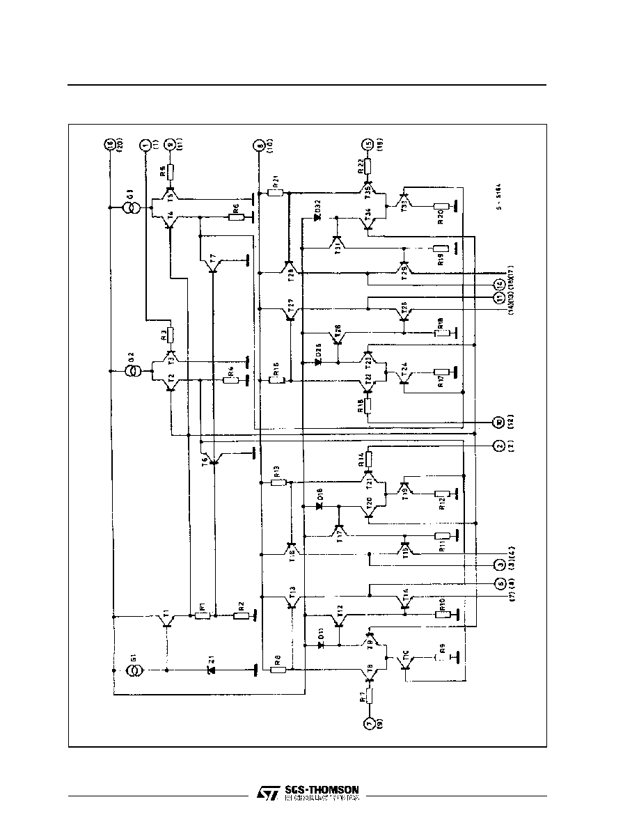
DESCRIPTION
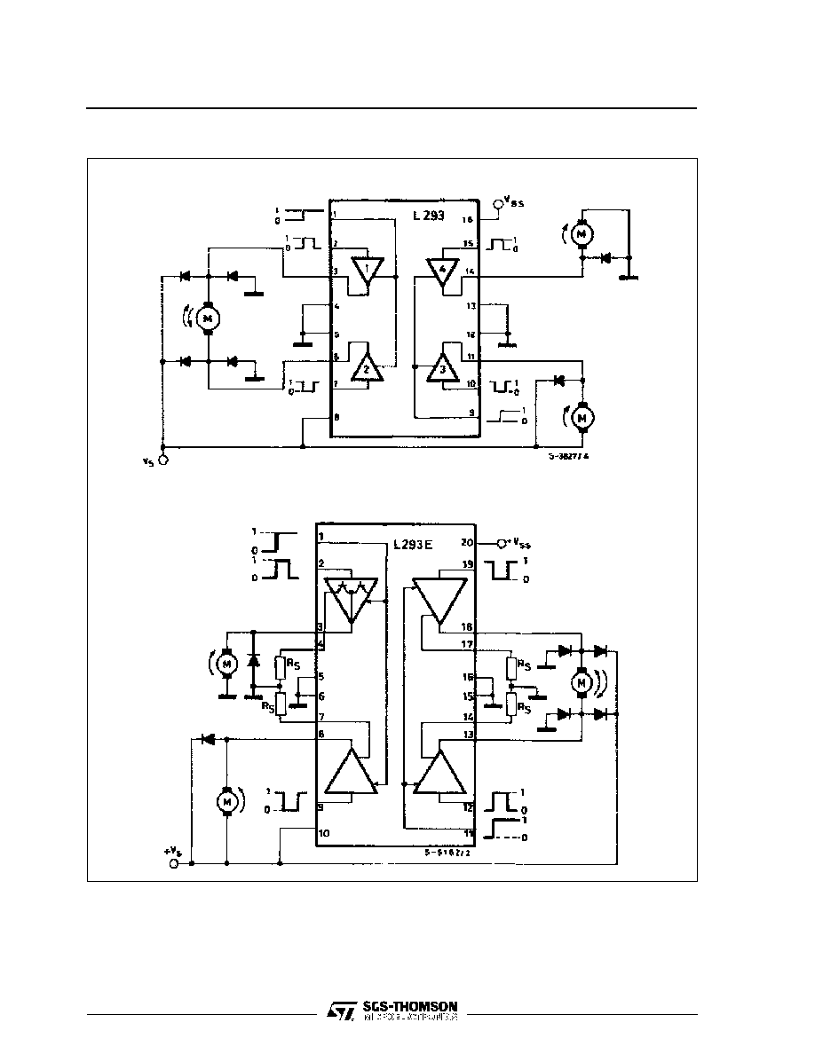
The L293B and L293E are quad push-pull drivers
capableof delivering output currents to 1A per chan-
nel. Each channel is controlledby a TTL-compatible
logic input and each pair of drivers (a full bridge) is
equipped with an inhibit input which turns off all four
transistors. A separate supply input is provided for
the logic so that it may be run off a lower voltage to
reduce dissipation.
Additionally, the L293E has external connection of
sensing resistors, for switchmode control.
The L293Band L293E are package in 16 and 20-pin
plastic DIPs respectively ; both use the four center
pins to conduct heat to the printed circuit board.
POWERDIP (16 + 2+ 2)
ORDERING NUMBER : L293E
DIP16
ORDERING NUMBER : L293B
PIN CONNECTIONS
DIP16 - L293B
POWERDIP (16+2+2) - L293E
1/12

THERMAL DATA
Symbol
Parameter
Value
Unit
R
th j-case
Thermal Resistance Junction-case
Max.
14
o
C/W
R
th j-amb
Thermal Resistance Junction-ambient
Max.
80
o
C/W
ELECTRICAL CHARACTERISTICS
For each channel, V
S
= 24V, V
SS
= 5V, T
amb
= 25
o
C, unless otherwise specified
Symbol
Parameter
Test Conditions
Min.
TYp.
Max.
Unit
V
s
Supply Voltage
V
ss
36
V
V
ss
Logic Supply Voltage
4.5
36
V
I
s
Total Quiescent Supply Current
V
i
= L
I
o
= 0
V
inh
= H
V
i
= H
I
o
= 0
V
inh
= H
V
inh
= L
2
16
6
24
4
mA
I
ss
Total Quiescent Logic Supply Current
V
i
= L
I
o
= 0
V
inh
= H
V
i
= H
I
o
= 0
V
inh
= H
V
inh
= L
44
16
16
60
22
24
mA
V
iL
Input Low Voltage
-03.
1.5
V
V
iH
Input High Voltage
V
SS
7V
V
ss
> 7V
2.3
2.3
V
ss
7
V
I
iL
Low Voltage Input Current
V
il
= 1.5V
-10
µ
A
I
iH
High Voltage Input Current
2.3V
V
IH
V
ss
- 0.6V
30
100
µ
A
V
inhL
Inhibit Low Voltage
-0.3
1.5
V
V
inhH
Inhibit High Voltage
V
SS
7V
V
ss
> 7V
2.3
2.3
V
ss
7
V
I
inhL
Low Voltage Inhibit Current
V
inhL
= 1.5V
-30
-100
µ
A
I
inhH
High Voltage Inhibit Current
2.3V
V
inh H
V
ss
- 0.6V
±
10
µ
A
V
CEsatH
Source Output Saturation Voltage
I
o
= -1A
1.4
1.8
V
V
CEsatL
Sink Output Saturation Voltage
I
o
= 1A
1.2
1.8
V
V
SENS
Sensing Voltage (pins 4, 7, 14, 17) (**)
2
V
t
r
Rise Time
0.1 to 0.9 V
o
(*)
250
ns
t
f
Fall Time
0.9 to 0.1 V
o
(*)
250
ns
t
on
Turn-on Delay
0.5 V
i
to 0.5 V
o
(*)
750
ns
t
off
Turn-off Delay
0.5 V
i
to 0.5 V
o
(*)
200
ns
*
See figure 1
**
Referred to L293E
ABSOLUTE MAXIMUM RATINGS
Symbol
Parameter
Value
Unit
V
s
Supply Voltage
36
V
V
ss
Logic Supply Voltage
36
V
V
i
Input Voltage
7
V
V
inh
Inhibit Voltage
7
V
I
out
Peak Output Current (non repetitive t = 5ms)
2
A
P
tot
Total Power Dissipation at T
ground-pins
= 80
o
C
5
W
T
stg
, T
j
Storage and Junction Temperature
≠40 to +150
o
C
TRUTH TABLE
V
i
(each channel)
V
o
V
inh
(
)
H
L
H
L
H
L
X (
o
)
X (
o
)
H
H
L
L
(*)
High output impedance
(**) Relative to the considerate channel
L293B - L293E
4/12
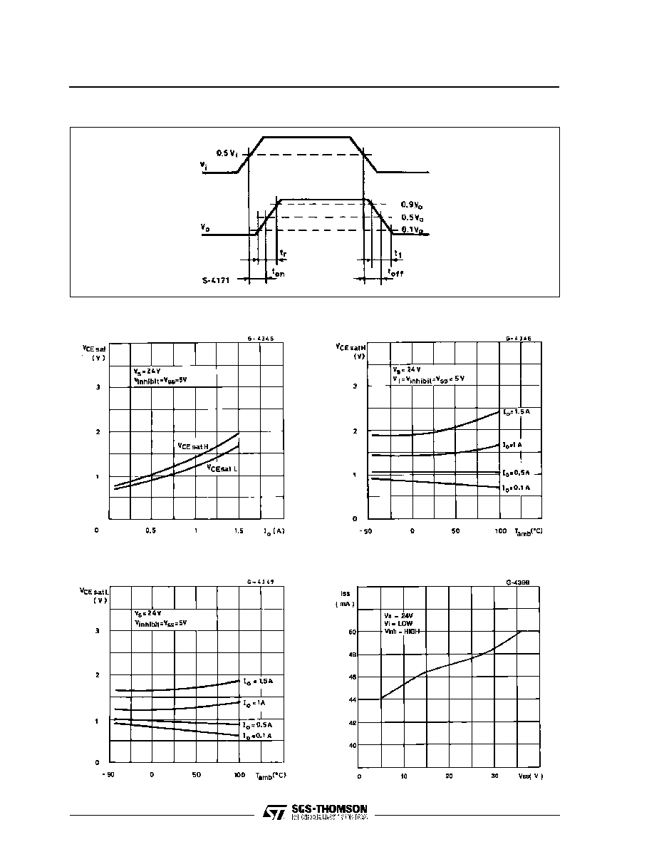
Figure 1 : Switching Timers
Figure 3 : Source Sa turation Voltage versus
Ambient Temperature
Figure 5 : Quiescent Logic Su pply Current
versus Logic Supply Voltage
Figure 2 : Saturation voltage versus Output
Current
Figure 4 : Sink Saturation Voltage versus
Ambient Temperature
L293B - L293E
5/12