 | –≠–ª–µ–∫—Ç—Ä–æ–Ω–Ω—ã–π –∫–æ–º–ø–æ–Ω–µ–Ω—Ç: L3100B | –°–∫–∞—á–∞—Ç—å:  PDF PDF  ZIP ZIP |

Application Specific Discretes
A.S.D.
TM
L3100B
L3100B1
DIL 8
OVERVOLTAGE AND OVERCURRENT
PROTECTION FOR TELECOM LINE
UNIDIRECTIONAL FUNCTION
PROGRAMMABLE BREAKDOWN VOLTAGE
UP TO 265 V
PROGRAMMABLE CURRENT LIMITATION
FROM 50 mA TO 550 mA
HIGH SURGE CURRENT CAPABILITY
I
PP
= 100A
10/1000
µ
s
FEATURES
Dedicated
to
sensitive
telecom
equipment
protection, this device can provide both voltage
protection and current limitation with a very tight
tolerance.
Its high surge current capability makes the L3100B
a reliable protection device for very exposed
equipment, or when series resistors are very low.
The breakdown voltage can be easily programmed
by using an external zener diode.
A multiple protection mode can also be performed
when using several zener diodes, providing each
line interface with an optimized protection level.
The current limiting function is achieved with the
use of a resistor between the gate N and the
cathode. The value of the resistor will determine
the level of the desired current.
DESCRIPTION
CCITT K17 - K20
10/700
µ
s
1.5
kV
5/310
µ
s
38
A
VDE 0433
10/700
µ
s
2
kV
5/200
µ
s
50
A
CNET
0.5/700
µ
s
1.5
kV
0.2/310
µ
s
38
A
COMPLIESWITH THE FOLLOWING STANDARDS :
Gate N
Gate P
Cathode
Anode
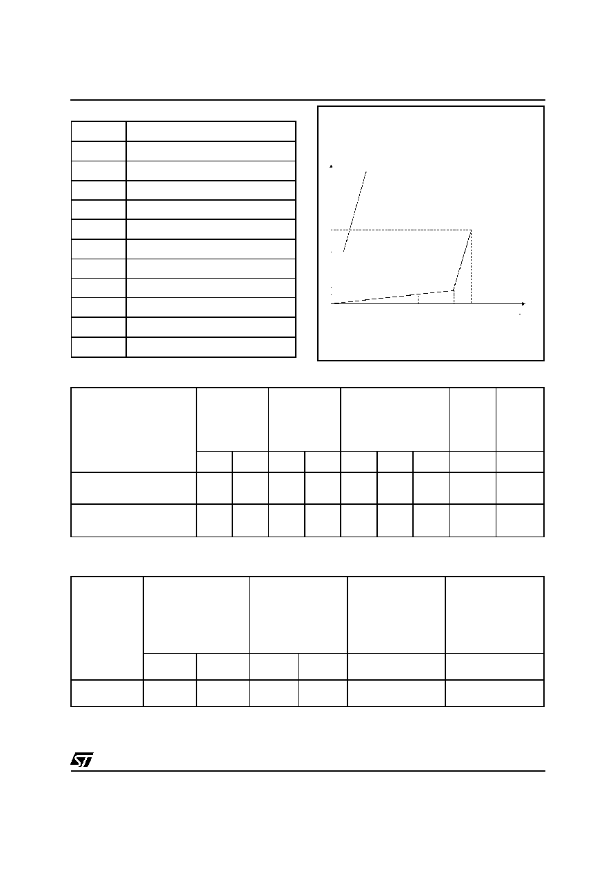
SCHEMATIC DIAGRAM
1
2
3
4
5
6
7
8
Gate N
NC
Gate P
Cathode
Anode
Anode
Anode
Anode
CONNECTION DIAGRAM
Æ
TM: ASD is trademarks of SGS-THOMSON Microelectronics.
September 1998 Ed : 3A
1/8

Symbol
Parameter
Value
Unit
I
PP
Peak pulse current (see note 1)
10/1000
µ
s
8/20
µ
s
100
250
A
I
TSM
Non repetitive surge peak on-state
current
tp = 10 ms
50
A
T
stg
T
j
Storage temperature range
Maximum operating junction temperature
- 40 to + 150
+ 150
∞
C
∞
C
T
L
Maximum lead temperature for soldering during 10s
230
∞
C
ABSOLUTE MAXIMUM RATINGS ( T
amb
= 25
∞
C)
Symbol
Parameter
Value
Unit
R
th (j-a)
Junction-to-ambient
80
∞
C/W
THERMAL RESISTANCE
Note 1 : Pulse waveform 10/1000
µ
s
100
50
% I
PP
t
t
r
p
0
t
L3100B/L3100B1
2/8
Type
V
GN
@ I
GN
= 200 mA
I
GN
@ V
AC
= 100V
V
RGN
@ I
G
= 1mA
I
GP
@ V
AC
= 100V
min.
max.
min.
max.
min.
max.
V
V
mA
mA
V
mA
L3100B/B1
0.6
1.8
30
200
0.7
150
Note 1 :
See the reference test circuits for IH, IBO and VBO parameters.
Note 2 :
VR = 5 V, F = 1MHz.
OPERATION WITH GATES
I
pp
I
BO
I
H
I
RM
V
RM
V
BR
V
BO
I
V
Symbol
Parameter
V
RM
Stand-off voltage
I
RM
Reverseleakagecurrent
V
BR
Breakdown voltage
V
BO
Breakover voltage
I
H
Holding current
I
BO
Breakover current
I
PP
Peak pulse current
V
GN
Gate voltage
I
GN
, I
GP
Triggering gate current
V
RGN
Reverse gate voltage
C
Capacitance
ELECTRICAL CHARACTERISTICS (T
amb
= 25
∞
C)
Type
I
RM
@ V
RM
V
BR
@ I
R
V
BO
@
I
BO
I
H
C
max.
min.
max.
min.
max.
min.
max.
note 1
note 1
note 2
µ
A
V
V
mA
V
mA
mA
mA
pF
L3100B
6
40
60
250
265
1
350
200
500
280
100
L3100B1
6
40
60
250
255
1
350
200
500
210
100
OPERATION WITHOUT GATE
L3100B/L3100B1
3/8

REFERENCE TEST CIRCUIT FOR I
BO
and V
BO
parameters:
220V
static
relay.
R1
R2
240
140
D.U.T
V BO
measure
IBO
measure
tp = 20ms
K
Transformer
220V/800V
5A
Auto
Transformer
220V/2A
Vout
FUNCTIONAL HOLDING CURRENT (I
H
) TEST CIRCUIT = GO - NOGO TEST.
R
- V
P
V
BAT
= - 48 V
Surge generator
D.U.T.
This is a GO-NOGO Test which allows to confirm the holding current (I
H
) level in a functional test
circuit.
This test can be performed if the reference test circuit can't be implemented.
TEST PROCEDURE :
1) Adjust the current level at the I
H
value by short circuiting the AK of the D.U.T.
2) Fire the D.U.T with a surge Current : Ipp = 10A , 10/1000
µ
s.
3) The D.U.T will come back to the OFF-State within a duration of 50 ms max.
TEST PROCEDURE :
Pulse Test duration (tp = 20ms):
- For Bidirectional devices = Switch K is closed
- For Unidirectional devices = Switch K is open.
V
OUT
Selection
- Device with V
BO
<
200 Volt
- V
OUT
= 250 V
RMS
, R
1
= 140
.
- Device with V
BO
200 Volt
- V
OUT
= 480 V
RMS
, R
2
= 240
.
L3100B/L3100B1
4/8

1E-2
1E-1
1E+0
1E+1
1E+2
1E+3
0
10
20
30
40
50
60
I
(A)
TSM
F=50Hz
Tj initial=25
∞
C
t(s)
Figure 1 : Surge peak current versus overload
duration.
0
10
20
30
40
50
60
70
0.98
0.99
1.00
1.01
1.02
1.03
1.04
Figure 3 : Relative variation of breakdown voltage
versus ambient temperature.
1
10
100
0
20
40
60
80
100
Figure 4 : Junction capacitance versus reverse
applied voltage.
0
10
20
30
40
50
60
70
0.7
0.8
0.9
1.0
1.1
1.2
Figure 2 : Relative variation of holding current
versus junction temperature.
L3100B/L3100B1
5/8