 | –≠–ª–µ–∫—Ç—Ä–æ–Ω–Ω—ã–π –∫–æ–º–ø–æ–Ω–µ–Ω—Ç: L3234 | –°–∫–∞—á–∞—Ç—å:  PDF PDF  ZIP ZIP |
This is advanced information on a new product now in development or undergoing evaluation. Details are subject to change without notice.
Janauary 1995
HIGHLY INTEGRATED SUBSCRIBER LINE
INTERFACE KIT FOR PABX AND KEY SYS-
TEM APPLICATIONS
IMPLEMENTS ALL KEY ELEMENTS OF THE
BORSCHT FUNCTION
INTEGRATED ZERO CROSSING BALANCED
RINGING INJECTION ELIMINATES EXTER-
NAL RELAY AND CENTRALISED RINGING
GENERATOR
ZERO NOISE INJECTED ON ADJACENT
LINES DURING RINGING SEQUENCE
LOW POWER IN STANDBY AND ACTIVE
MODES
BATTERY FEED WITH PROGRAMMABLE
LIMITING CURRENT
PARALLEL LATCHED DIGITAL INTERFACE
SIGNALLING
FUNCTIONS
(OFF
HOOK,
GND-KEY)
LOW NUMBER OF EXTERNAL COMPO-
NENTS
INTEGRATED THERMAL PROTECTION
INTEGRATED OVER CURRENT PROTEC-
TION
0
∞
C TO 70
∞
C: L3234/L3235
-40
∞
C TO 85
∞
C: L3234T/L3235T
DESCRIPTION
The L3234/L3235 is a highly integrated SLIC KIT
targeted to PABX and key system applications
The kit integrates the majority of functions re-
quired
to
interface
a
telephone line.
The
L3234/L3235 implements the main features of the
broths function:
- Battery Feed (Balanced Mode)
- Ringing Injection
- Signalling Detection
- Hybrid Function
The Kit comprises 2 devices, the L3234 ringing
injector fabricated in Bipolar in 140V Technology.
Its function is to amplify and inject in balanced
mode with zero crossing the ringing signal. The
device requires an external positive supply of
100V and a low level sinusoid of approx.
950mVrms. The L3235 Line Feeder is integrated
in 60V Bipolar Technology. The L3235 provides
battery feed to the line with programmable current
limitation. The two to four wire voice frequency
signal conversion is implemented by the L3235
and line terminating and balance impedances are
externally programmable. The L3234/L3235 kit is
designed for low power dissipation. In a short
loop condition the extra power is dissipated on an
external transistor. The Kit is controlled by five
wire parallel bus and interfaces easily to all first
and programmable second generation COMBOS.
(see figg. 1 and 2)
HEPTAWATT
ORDERING NUMBER: L3234
PLCC28
ORDERING NUMBER: L3235
L3234
L3235
HIGHLY INTEGRATED SLIC KIT TARGETED TO PABX
AND KEY SYSTEM APPLICATIONS
1/26
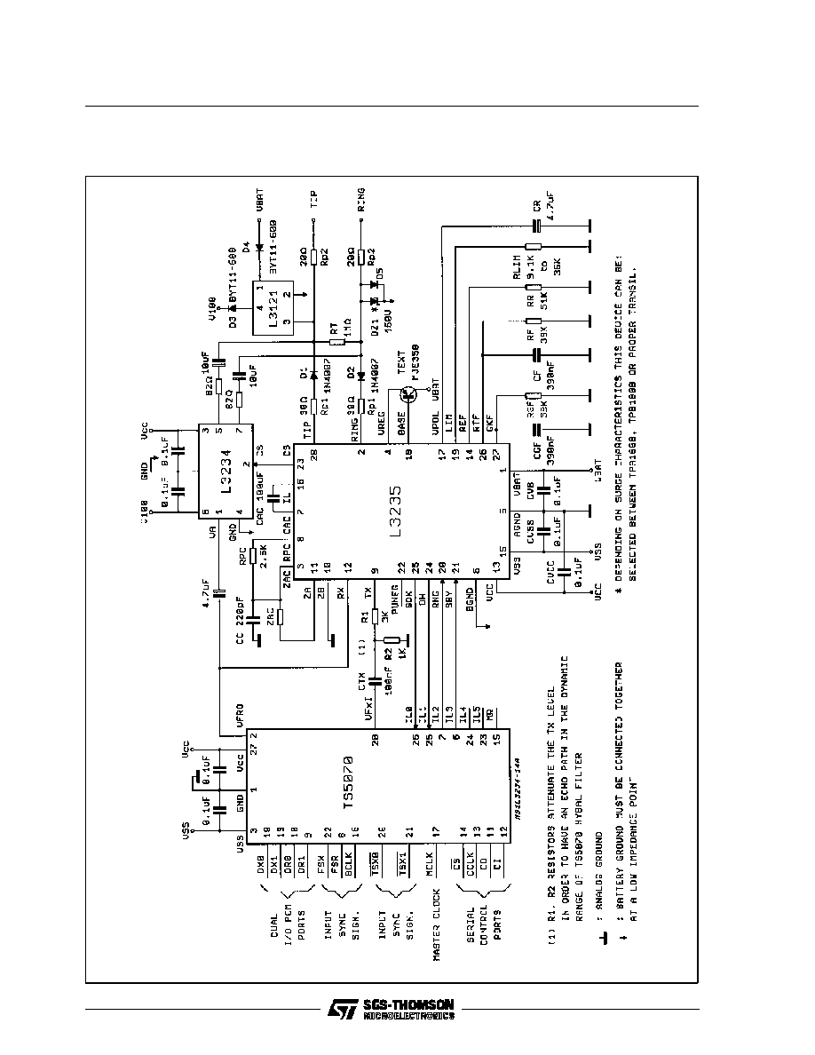
Figure 1: Typical Application Circuit with Second Generation COMBO for Complete Subscriber Circuit
(Protection-SLIC-COMBO)
L3234 - L3235
2/26

Figure 2: Typical Application Circuit with First Generation COMBO for Complete Subscriber Circuit
(Protection-SLIC-COMBO)
L3234 - L3235
3/26
DESCRIPTION
The L3234 is a monolithic integrated circuit which
is part of a kit of solid state devices for the sub-
scriber line interface. The L3234 sends a ringing
signal into a two wires analog telephone line in
balanced mode. The AC ringing signal amplitude
is up to 60Vrms, and for that purpose a positive
supply voltage of +100V shall be available on the
subscriber card.
The L3234 receives a low amplitude ringing sig-
nal (950mVrms) and provide the voltage/current
amplification (60Vrms/70mA) when the enable in-
put is active (CS > 2V). In disable mode (CS <
0.8V) the power consumption of the chip is very
low (<14mW).
The circuit is designed with a high voltage bipolar
technology (V
CEO
> 140V / V
CBO
> 250V).
The package is a moulded plastic power package
(Heptawatt) suitable also for surface mounting.
HEPTAWATT
BLOCK DIAGRAM
L3234
Solid State Ringing Injector
L3234 - L3235
4/26

1
2
3
4
5
6
7
D94TL131
OUT2
V100
OUT1
GND
VCC
CS
VA
PIN CONNECTION (Top view)
ABSOLUTE MAXIMUM RATINGS
Symbol
Parameter
Value
Unit
V100
Positive Power Supply Voltage
+120
V
V
CC
5V Power Supply Voltage
5.5
V
V
A
Low Voltage Ringing Signal (with V100 = 120Vdc)
1.4
Vrms
CS
Logical Ring Drive Input
V
CC
T
j
Max. Junction Temperature
150
o
C
T
stg
Storage Temperature
-55 to +150
o
C
OPERATING RANGE
Symbol
Parameter
Value
Unit
V100
High Power Supply Voltage
95 to 105
V
V
CC
Low Power Supply Voltage
5
±
5%
V
V
A
Low Voltage Ringing Signal
600 to 950
within 10Hz - 100Hz
Vrms
T
op
Operating Temperature for L3234
L3234T
0 to 70
-40 to 85
∞
C
∞
C
T
jop
Max. Junction Operating Temperature (due to thermal protection)
130
∞
C
Note: Operating ranges define those limits between which the functionality of the device is guaranteed.
THERMAL DATA
Symbol
Description
Value
Unit
R
th j-case
R
th j-amb
Thermal Resistance Junction-case
Thermal Resistance Junction-ambient
Max.
Max.
4
50
o
C/W
o
C/W
PIN DESCRIPTION
Pin
Name
Description
1
VA
Low Voltage Ringing Signal Input
2
CS
Logical Ring Drive Input
3
V
CC
+5V Low Power Supply
4
GND
Common Analog-Digital Ground
5
OUT1
Ringing Signal Output
6
V100
+100V High Power Supply
L3234 - L3235
5/26