 | –≠–ª–µ–∫—Ç—Ä–æ–Ω–Ω—ã–π –∫–æ–º–ø–æ–Ω–µ–Ω—Ç: L3240D1 | –°–∫–∞—á–∞—Ç—å:  PDF PDF  ZIP ZIP |

L3240
June 1993
ELETRONIC TWO-TONE RINGER
.
LOW CURRENT CONSUMPTION, IN ORDER
TO ALLOW THE PARALLEL OPERATION OF 4
DEVICES
.
INTEGRATED RECTIFIER BRIDGE
WITH
ZENER DIODES TO PROTECT AGAINST
OVERVOLTAGES
.
LITTLE EXTERNAL CIRCUITRY
.
TONE AND SWITCHING FREQUENCIES AD-
JUSTABLE BY EXTERNAL COMPONENTS
.
INTEGRATED VOLTAGE AND CURRENT
HYSTERESIS
.
COMPLEMENTARY OUTPUT CONFIGURA-
TION
DESCRIPTION
L3240 is a monolithic integrated circuit designed to
replace the mechanical bell in telephone sets, in
connectionwith an electro acoustical converter. The
device can drive either directly a piezo ceramic con-
verter (buzzer) or a small loudspeaker. In this case
a transformer is needed. The two tone frequencies
generated are switched by an internal oscillator in a
fast sequenceand made audible across output am-
plifiers in the transducer ; both tone frequencies and
the switching frequency can be externally adjusted.
The supply voltage is obtained from the AC ring sig-
nal and the circuit is designed so that noise on the
line or variations of the ringing signal cannot affect
the correct operation of the devices.
The output bridge configuration allows to use a high
impedance transducer with acoustical results much
better than in a single ended configuration.
The two outputs can also be connected inde-
pendently to
different
converters
or
actua-
tors (acoustical, opto, logic).
PIN CONNECTION ( top view)
Minidip
SO8
ORDERING NUMBERS : L3240B1 (Minidip)
L3240D1 (SO8)
1/6

BLOCK DIAGRAM
ABSOLUTE MAXIMUM RATINGS
Symbol
Parameter
Value
Unit
V
AB
Calling Voltage (f = 50 Hz) Continuous
120
V
RMS
V
AB
Calling Voltage (f = 50 Hz) 5s N/10s OFF
200
V
RMS
DC
Supply Current
30
mA
T
op
Operating Temperature
≠ 20, + 70
o
C
T
stg
Storage and Junction Temperature
≠ 65, + 150
o
C
THERMAL DATA
Symbol
Parameter
Value
Unit
R
th j-amb
Thermal Resistance Junction-ambient
Max.
100
o
C/W
ELECTRICAL CHARACTERISTICS
(T
amb
= 25
o
C ; V
S
= applied between pins 7-2 ;otherwise specified)
Symbol
Parameter
Test Conditions
Min.
Typ.
Max.
Unit
V
s
Supply Voltage
26
V
I
B
Current Consumption Without Load (Pins 8-1)
V
8-1
= 16.5 to 29.5 V
1.5
1.8
mA
V
ON
Activation Voltage
12
13.5
V
V
OFF
Sustaining Voltage
7.8
9.3
V
R
D
Differential Resistance in OFF Condition (Pins 8-1)
6.4
k
V
OUT
Output Voltage Swing
V
s
≠ 5
V
I
OUT
Short Circuit Current (pins 5-6)
V
s
= 20 V
35
mA
V
s
Voltage Drop between Pins 8-1 and Pins 7-2
3
V
L3240
2/6
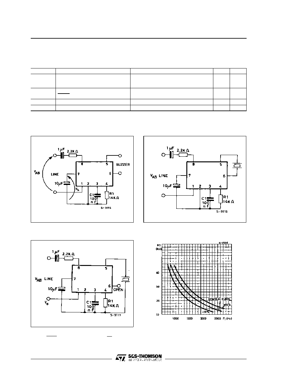
Figure 1 : Test Circuit.
Figure 2 : Typical Application with Balanced
Output.
Figure 3 : Application Compatible with LS1240
(single ended output).
Figure 4 : F
1
Out vs. R
1
.
3.56 x 10
4
F
1
R
1
x
(
1 ≠ 0.12 x ln
)
F
1
(HZ)
2543
f
2
= 0.725 f
1
750
f
SWEEP
=
C1 (nF)
ELECTRICAL CHARACTERISTICS
(T
amb
= 25
o
C ; V
S
= applied between pins 7-2 ;otherwise specified)
AC OPERATION
Symbol
Parameter
Test Conditions
Min.
Typ.
Max.
Unit
Output Frequencies
Fout 1
Fout 2
V
s
= 26 V, R
1
= 14 K
V
s
= 0 V
V
s
= 6 V
2,29
1.6
2,8
2.1
kHz
Fout 1
Fout 2
1.33
1.43
Programming Resistor Range
8
56
k
Sweep Frequency
R
1
= 14k
, C1 =100nF
5.25
7,5
9.75
Hz
L3240
3/6
MINIDIP PACKAGE MECHANICAL DATA
DIM
mm
inch
Min.
Typ.
Max.
Min.
Typ.
Max.
A
3.32
0.131
a1
0.51
0.020
B
1.15
1.65
0.045
0.065
b
0.356
0.55
0.014
0.022
b1
0.204
0.304
0.008
0.012
D
10.92
0.430
E
7.95
9.75
0.313
0.384
e
2.54
0.100
e3
7.62
0.300
e4
7.62
0.300
F
6.6
0260
i
5.08
0.200
L
3.18
3.81
0.125
0.150
Z
1.52
0.060
DIP8.TBL
L3240
4/6

SO8 PACKAGE MECHANICAL DATA
DIM
mm
inch
Min.
Typ.
Max.
Min.
Typ.
Max.
A
1.75
0.069
a1
0.1
0.25
0.004
0.010
a2
1.65
0.065
a3
0.65
0.85
0.026
0.033
b
0.35
0.48
0.014
0.019
b1
0.19
0.25
0.007
0.010
C
0.25
0.5
0.010
0.020
c1
45
o
(typ.)
D
4.8
5.0
0.189
0.197
E
5.8
6.2
0.228
0.244
e
1.27
0.050
e3
3.81
0.150
F
3.8
4.0
0.150
0.157
L
0.4
1.27
0.016
0.050
M
0.6
0.024
S
8
o
(max.)
SO8.TBL
L3240
5/6

Information furnished is believed to be accurate and reliable. However, SGS-THOMSON Microelectronics assumes no responsibility for
the consequences of use of such information nor for any infringement of patents or other rights of third parties which may result from its
use. No license is granted by implication or otherwise under any patent or patent rights of SGS-THOMSON Microelectronics. Specifica-
tions mentioned in this publication are subject to change without notice. This publication supersedes and replaces all information pre-
viously supplied. SGS-THOMSON Microelectronics products are not authorized for use as critical components in life support devices or
systems without express written approval of SGS-THOMSON Microelectronics.
©
1994 SGS-THOMSON Microelectronics - All Rights Reserved
SGS-THOMSON Microelectronics GROUP OF COMPANIES
Australia - Brazil - France - Germany - Hong Kong - Italy - Japan - Korea - Malaysia - Malta - Morocco - The Netherlands
Singapore - Spain - Sweden - Switzerland - Taiwan - Thaliand - United Kingdom - U.S.A.
L3240
6/6