 | –≠–ª–µ–∫—Ç—Ä–æ–Ω–Ω—ã–π –∫–æ–º–ø–æ–Ω–µ–Ω—Ç: L3281 | –°–∫–∞—á–∞—Ç—å:  PDF PDF  ZIP ZIP |

L3281
LOW VOLTAGE TELEPHONE SPEECH CIRCUITS
PRELIMINARY DATA
OPERATION DOWN TO 1.6V / 6.5mA
DTMF & BEEP TONE INPUTS
EXTERNAL MUTING FOR EARPHONE AND
MICROPHONE
SUITABLE FOR DYNAMIC EARPHONE AND
DYNAMIC OR ELECTRET MICROPHONE
AGC CONTROL ON BOTH SENDING AND
RECEIVING
DESCRIPTION
The L3281 is an electronic speech circuit devel-
oped to replace hybrid circuits in telephone sets
that can be operated in parallel with other
phones.
This is advanced information on a new product now in development or undergoing evaluation. Details are subject to change without notice.
June 1993
BLOCK DIAGRAM
DIP14
ORDERING NUMBERS:
L3281AB
L3281AD1
SO14
1/10
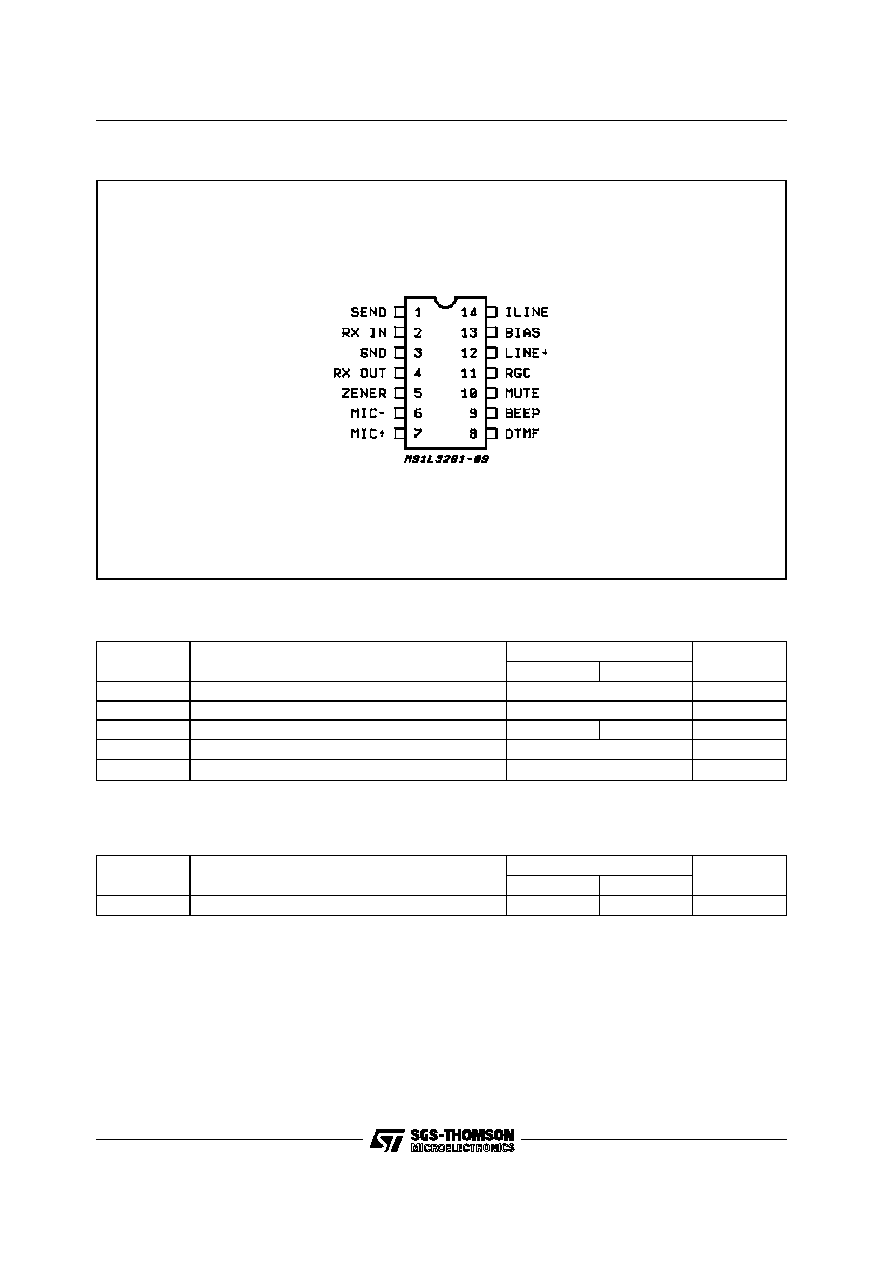
PIN CONNECTION (top view)
THERMAL DATA
Symbol
Parameter
Value
Unit
DIP-14
SO-14
R
th j-amb
Thermal Resistance Junction Ambient Max
90
130
∞
C/W
ABSOLUTE MAXIMUM RATINGS
Symbol
Parameter
Value
Unit
DIP-14
SO-14
V
L
Line Voltage (3 ms pulse)
15
V
I
L
Line Current
150
mA
P
tot
Total Power Dissipation, T
amb
= 55
∞
C
1.0
0.6
W
T
op
Operating Temperature
≠ 20 to 55
∞
C
T
j
Junction Temperature
≠ 65 to 150
∞
C
L3281
2/10

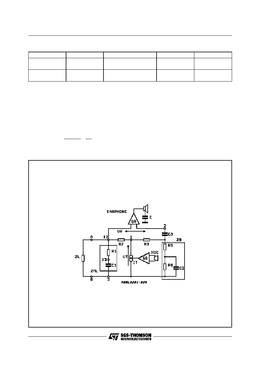
TEST CIRCUITS
Figure 1.
Figure 2.
Figure 3.
L3281
3/10
ELECTRICAL CHARACTERISTICS I
L
= 20 to 100mA; R4 =( 51
// diode) + 33
;
T = 25
∞
C; f = 1kHz; Unless Otherwise Specified
Symbol
Parameter
Test Condition
Min.
Typ.
Max.
Unit
V
l
Line Voltage
I
L
= 6.5mA
I
L
= 20mA
I
L
= 50mA
I
L
= 80mA
1.65
3.4
6.0
8
3.7
6.5
9.5
V
V
V
V
CMRR
Common Mode Rej. Ratio
50
dB
G
tx
Sending Gain
V
mi
= 10mV; I
L
= 20mA
30
31.5
33
dB
DG
tx
Delta Sending Gain
V
mi
= 10mV; I
L
= 70mA
≠ 7.2
≠5.7
≠4.2
dB
THD
tx
Sending Distortion
V
so
= 700mV; I
L
= 20mA
5
%
N
tx
Sending Noise
V
mi
= 0V; I
L
= 50mA
≠ 70
dB
Z
ml
Mic. Input Impedance
V
mi
= 10mV
40
k
G
rx
Receiving Gain
I
L
= 20mA; V
ri
= 0.2V
≠ 10.7
≠ 9.2
≠ 7.7
dB
DG
rx
Delta Receiving Gain
I
L
= 70mA; V
ri
= 0.2V
≠ 7.2
≠ 5.7
≠ 4.2
dB
THD
rx
Receiving Distortion
V
ro
= 350mV; Load = 350
V
ro
= 300mV; I
L
= 10 mA
5
5
%
%
N
rx
Receiving Noise
V
ri
= 0V
100
µ
V
Z
ro
Rec. Output Impedance
Load = 200
; V
ro
= 50V
10
Sidetone
V
mi
= 10mV
10
20
dB
Z
m
Line Match. Impedance
V
ri
= 0.2V
500
600
700
V
so
Sending Output Voltage
I
L
= 6.5mA; THD = 5%
100
mV
I
ro
Receiving Output Current
I
L
= 6.5mA; THD = 5%
0.5
mAp
MU
lo
Mute Input Low
Dialing Mode
50
100
µ
A
MU
hl
Mute Input Open
Speaking Mode
1
µ
A
G
mf
DTMF Gain
V
mf IN
= 10mV
14.5
16
17.5
dB
R
mf
DTMF Input Impedance
5
10
k
THD
mf
DTMF Distortion
V
mf LN
= 140mV
5
%
G
beep
Beeptone Gain
V
beep IN
= 25mV
8.5
dB
R
beep
Beeptone Input Impedance
5.5
8
k
THD
beep
Beeptone Distortion
V
beep IN
= 100mV; I
L
= 20mA
0.5
5
%
V
z
Zener Voltage (Pin 5)
I
z
= 1 mA
4.2
5.1
6.2
V
I
leak
Leakage Current,V
pin5
= 3V
20
µ
A
L3281
4/10
CIRCUIT DESCRIPTION
TWO TO FOUR WIRE CONVERSION
The L3281AB is based on a Wheastone bridge
configuration. To balance the bridge the following
relation must be satisfied:
ZI / /
Zm
Zb
=
R2
R3
The AC signal from the microphone is sent to one
diagonal of the bridge (pins 1 and 3). A small per-
centage of the signal power is lost on Zb (being
Zb > (Zm//Zi)); the main part is sent to the line via
R2.
In receiving mode, the AC signal coming from the
LINE is sensed across the second diagonal of the
bridge (pins 12 and 2).
The impedance Zm and Zb can be complex.
LOGIC OF MUTE SWITCHING
MUTE
DTMF
BEEP
MIC IMP
RX IMP
LOW
ACTIVE TO LINE
ACTIVE TO EARPHONE
MUTED
MUTED
(DIAL)
OUTPUT
OUTPUT
OPEN
ACTIVE TO LINE
ACTIVE TO EARPHONE
ACTIVE
ACTIVE
(SPEECH)
OUTPUT
OUTPUT
Figure 4: 2/4 Wire Conversion
L3281
5/10

DC CHARACTERISTIC
The fig.5 shows the equivalent simplified circuit of
the DC regulator that provides to give the oppor-
tune DC impedance Zdc.
VL
=
Idc
Z4
RB
(
RA
+
RB
)
+
VD
+
VR1
VL
=
(
Idc
Z4
)
RA
RB
+
1
+
VD
+
VR1
since RA = RB
VL
=
(
Idc
Z4
2
)
+
VD
+
VR1
When IL 18 mA and considering neglectible the
VD + VR1 variation versus line current :
ZDC
=
VL
Idc
=
2
Z4
At IL = 6.5 mA no current flows through Z4 but
only in the rest of the circuit for internal biasing
(Io;Ia). The bias current Io is fixed by the resistor
R2. The line voltage in this case is :
VL = Ia RA + VR1 = 1.6 V
The Fig.6 shows the DC characteristic (voltage
between pin 12 and pin 3 versus line current).
The device own an equivalent zener voltage at
pin 5 that can be used as supply voltage for elec-
tret microphone (see Block Diagram).
The value of the resistor R2 and the capacitor C2
should be chosen in order to not affect the AC
line inpedance. The Fig.7 shows the zener
equivalent.
The zener voltage will be:
Vz
=
70K
13.6K
+
1
Vbe
It is possible to supply 1mA to the electrete volt-
age if VL > (1mA + Iz)
Rz + Vz
Figure 5: Equivalent Simplified Circuit
Figure 6: Low Voltage Speech Circuit.
Figure 7: Zener Equivalent.
L3281
6/10

AC CHARACTERISTIC
The AC Impedance measured at line terminals is
equal to:
Zm
= (
R1
+
1
jwC1
)
/ /
(
R2
+
R3
+
Zb
)
The value of the capacitor C1 must be In the
range of 22
µ
F to 100
µ
F.
The external resistor R1 can be replaced by a re-
sistor/capacitor network in order to realize a com-
plex Impedance Zm.
TRANSMITTING CIRCUIT
The first block of the TX stage is basically a differ-
ential amplifier which converts voltage to current.
The inputs are internally polarized at 300 mVdc.
The differential Input impedance is 60 K
to allow
a good matching to microphone. The AGC in TX
is function of voltage at pin 14 in order to de-
crease to max gain of 5.5dB to 6.0dB when the
line current increases.
RECEIVING CIRCUIT
Fig.9 shows the equivalent receiving circuit. The
differential input of RX signal across R2+R3 is
transferred to the AGC block when the mute sig-
nal (pin 10) is not active.
The AGC in RX is a function of the voltage at pin
14 and decreases the gain when the line current
increases (5.5dB to 6.0dB).
The final stage is a single ended amplifier with
low output impedance optimized to drive mag-
netic/dynamic transducers.
Figure 8: Equivalent Transmitting Circuit.
Figure 9: Equivalent Receiving Circuit.
L3281
7/10
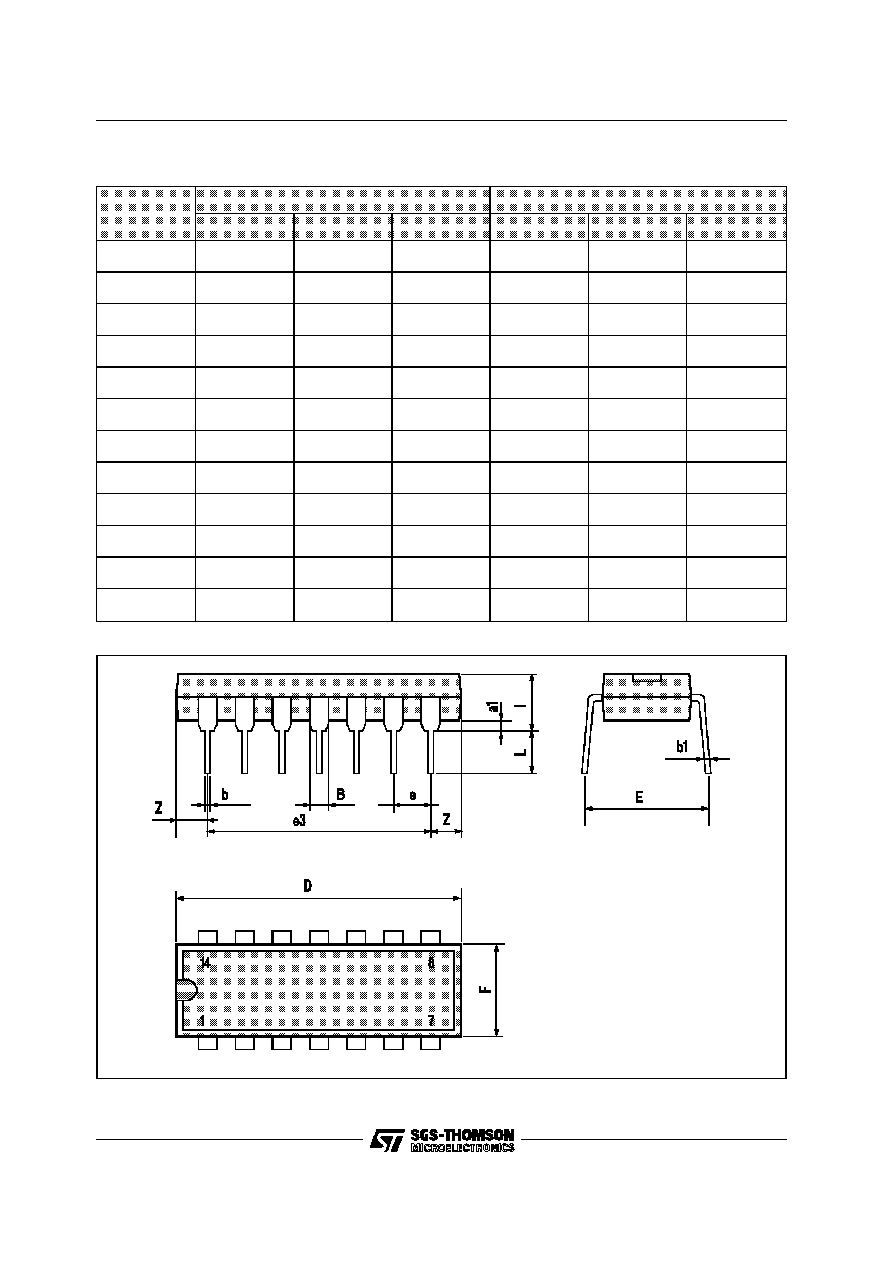
DIP14 PACKAGE MECHANICAL DATA
DIM.
mm
inch
MIN.
TYP.
MAX.
MIN.
TYP.
MAX.
a1
0.51
0.020
B
1.39
1.65
0.055
0.065
b
0.5
0.020
b1
0.25
0.010
D
20
0.787
E
8.5
0.335
e
2.54
0.100
e3
15.24
0.600
F
7.1
0.280
I
5.1
0.201
L
3.3
0.130
Z
1.27
2.54
0.050
0.100
L3281
8/10

SO14 PACKAGE MECHANICAL DATA
DIM.
mm
inch
MIN.
TYP.
MAX.
MIN.
TYP.
MAX.
A
1.75
0.069
a1
0.1
0.2
0.004
0.008
a2
1.6
0.063
b
0.35
0.46
0.014
0.018
b1
0.19
0.25
0.007
0.010
C
0.5
0.020
c1
45
∞
(typ.)
D
8.55
8.75
0.336
0.344
E
5.8
6.2
0.228
0.244
e
1.27
0.050
e3
7.62
0.300
F
3.8
4.0
0.15
0.157
L
0.5
1.27
0.020
0.050
M
0.68
0.027
S
8
∞
(max.)
L3281
9/10

Information furnished is believed to be accurate and reliable. However, SGS-THOMSON Microelectronics assumes no responsibility for the
consequences of use of such information nor for any infringement of patents or other rights of third parties which may result from its use. No
license is granted by implication or otherwise under any patent or patent rights of SGS-THOMSON Microelectronics. Specifications mentioned
in this publication are subject to change without notice. This publication supersedes and replaces all information previously supplied.
SGS-THOMSON Microelectronics products are not authorized for use as critical components in life support devices or systems without express
written approval of SGS-THOMSON Microelectronics.
©
1994 SGS-THOMSON Microelectronics - All Rights Reserved
SGS-THOMSON Microelectronics GROUP OF COMPANIES
Australia - Brazil - France - Germany - Hong Kong - Italy - Japan - Korea - Malaysia - Malta - Morocco - The Netherlands
Singapore - Spain - Sweden - Switzerland - Taiwan - Thaliand - United Kingdom - U.S.A.
L3281
10/10