
L387A
October 1991
VERY LOW DROP 5V REGULATOR WITH RESET
.
PRECISE OUTPUT VOLTAGE (5 V
±
4 %)
.
VERY LOW DROPOUT VOLTAGE
.
OUTPUT CURRENT IN EXCESS OF 500mA
.
POWER-ON,
POWER-OFF
INFORMATION
(RESET FUNCTION)
.
HIGH NOISE IMMUNITY ON RESET DELAY
CAPACITOR
ORDERING NUMBER : L387A
Pentawatt
Æ
The L387A is a very low drop voltage regulator in
a Pentawatt
Æ
package specially designed to pro-
vide stabilized 5V supplies in consumer and in-
dustrial applications. Thanks to its very low in-
put/output voltage drop this device is very useful
in battery powered equipment, reducing con-
sumption and prolonging battery life. A reset out-
put makes the L387A particularly suitable for mi-
croprocessor systems. This output provides a re-
set signal when power is applied (after an exter-
nal programmable delay) and goes low when
DESCRIPTION
power is removed, inhibiting the microprocessor.
An hysteresis on reset delay capacitor raises the
immunity to the ground noise.
APPLICATION CIRCUIT
* Min 33
µ
F and max. ESR
3
over temperature range.
ABSOLUTE MAXIMUM RATINGS
Symbol
Parameter
Value
Unit
V
i
D.C. Input Voltage
35
V
T
j
, T
stg
Junction and Storage Temperature Range
≠55 to 150
∞
C
1/6

ELECTRICAL CHARACTERISTICS (refer to the test circuit, V
i
= 14.4 V, T
j
= 25
∞
C, C
o
= 100
µ
F;
unless otherwise specified)
Symbol
Parameter
Test Conditions
Min.
Typ.
Max.
Unit
V
o
Output Voltage
I
o
= 5 mA to 500 mA T
j
= 25
∞
C
≠ 40
T
j
125
∞
C
4.80
4.75
5.00
5.00
5.20
5.25
V
V
V
I
Operating Input Voltage
(*), Over Full T Range (≠ 40 to 125
∞
C)
(see note **)
26
V
V
o
Line Regulation
V
i
= 6 V to 26 V
I
o
= 5 mA
5
50
mV
V
o
Load Regulation
I
o
= 5 mA to 500 mA
15
60
mV
V
I
≠ V
o
Dropout Voltage
V
O
= V
O NOM
≠ 100 mV
I
o
= 350 mA
I
o
= 500 mA
0.40
0.60
0.65
0.8
V
V
I
q
Quiescent Current
I
o
= 0 mA
I
o
= 150 mA
I
o
= 350 mA
I
o
= 500 mA
5
20
60
100
15
35
100
160
mA
mA
mA
mA
V
i
= 6.2 V
I
o
= 500 mA
160
180
mA
V
o
T
Temperature Output
Voltage Drift
≠ 0.5
mV/
∞
C
SVR
Supply Voltage Rejection
I
o
= 350 mA
f = 120 Hz
C
o
= 100
µ
F
V
i
= 12 V
±
5 V
pp
60
I
SC
Output Short Circuit
Current
1.2
1.6
A
V
R
Reset Output Voltage
I
R
= 3 mA
1 < V
o
< 4.70 V
I
R
= 16 mA
1.5 < V
o
< 4.75 V
Over Full T (≠ 40
∞
C
T
j
125
∞
C)
0.5
0.8
V
V
I
R
Reset Output Leakage
Current
V
o
in Regulation V
R
= 5V
Over Full T Range
50
µ
A
t
d
Delay Time for Reset
Output
Cd = 100 nF
Over Full T Range
25
ms
V
RT (off)
V
o
@ Reset out H to L Transition, Over
Full T Range
4.75
V
o
≠ 0.15
V
I
C4
Charging Current
(current generator)
V
4
= 3 V
10
20
30
µ
A
V
RT (on)
Power on
V
o
Threshold
V
o
@ Reset out L to H Transition , Over
Full T Range
V
RT (off)
+ 0.05 V
V
o
≠ 0.04 V
V
V
4
Comparator Threshold
(pin 4)
V
4
@ Reset out H to L Transition
3.2
3.9
V
V
4
@ Reset out L to H Transition
3.7
4.3
V
V
H
Hysteresis Voltage
Over Full T Range
450
mV
(*)
For a DC voltage 26 < Vi < 37 V the device is not operating.
(**) Design limits are guaranteed (but not 100 % production tested) over the indicated temperature and supply voltage ranges.
These limits are not used to calculate outgoing quality levels.
L387A
3/6
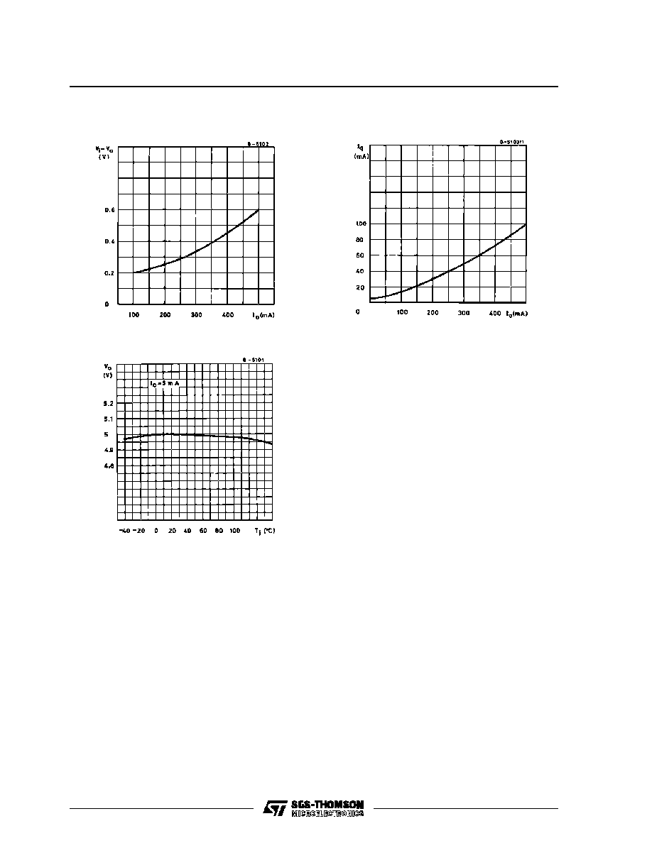
Figure 1 : Dropout Volta ge vs. Output Current.
Figure 2 : Quiescent Current vs. Output
Current.
Figure 3 : Output Voltage vs. Temperature.
L387A
4/6

