 | –≠–ª–µ–∫—Ç—Ä–æ–Ω–Ω—ã–π –∫–æ–º–ø–æ–Ω–µ–Ω—Ç: L4903 | –°–∫–∞—á–∞—Ç—å:  PDF PDF  ZIP ZIP |
L4903
DUAL 5V REGULATOR
WITH RESET AND DISABLE FUNCTIONS
July1993
PRELIMINARY DATA
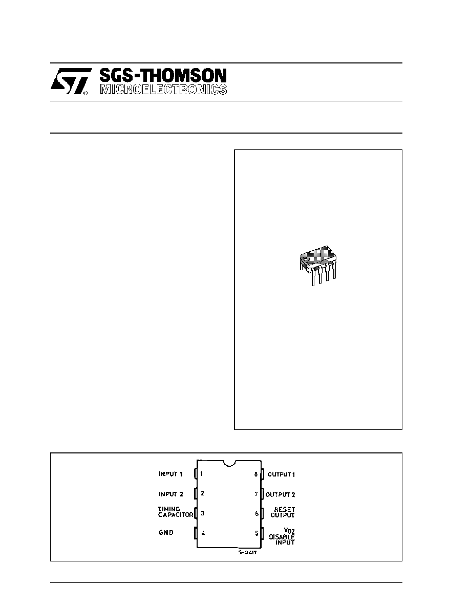
PIN CONNECTION
Minidip
ORDERING NUMBERS : L4903
.
OUTPUT CURRENTS : I
01
= 50mA
I
02
= 100mA
.
FIXED PRECISION OUTPUT VOLTAGE
5V
±
2 %
.
RESET FUNCTION CONTROLLED BY INPUT
VOLTAGE AND OUTPUT 1 VOLTAGE
.
RESET
FUNCTION
EXTERNALLY
PRO-
GRAMMABLE TIMING
.
RESET OUTPUT LEVEL RELATED TO OUT-
PUT 2
.
OUTPUT 2 INTERNALLY SWITCHED WITH
ACTIVE DISCHARGING
.
OUTPUT 2 DISABLE LOGICAL INPUT
.
LOW LEAKAGE CURRENT, LESS THAN 1
µ
A
AT OUTPUT 1
.
INPUT OVERVOLTAGE PROTECTION UP TO
60V
.
RESET OUTPUT NORMALLY LOW
.
OUTPUT TRANSISTORS SOA PROTECTION
.
SHORT CIRCUIT AND THERMAL OVER-
LOAD PROTECTION
DESCRIPTION
The L4903 is a monolithic low drop dual 5 V regu-
lator designed mainly for supplying microprocessor
systems.
Reset, data save functions and remote switch
on/off control can be realized.
1/8

BLOCK DIAGRAM
SCHEMATIC DIAGRAM
PIN FUNCTIONS
N
∞
Name
Function
1
Input 1
Low Quiescent Current 50mA Regulator Input
2
Input 2
100mA Regulator Input.
3
Timing
Capacitor
If Reg. 2 is switched-ON the delay capacitor is charged with a 10
µ
A constant current. When
Reg. 2 is switched-OFF the delay capacitor is discharged.
4
GND
Common Ground
5
Disable Input
A high level (> V
DT
) disables output Reg. 2.
6
Reset Output
When pin 3 reaches 5V the reset output is switched low.
Therefore t
RD
= C
t
(
5V
10
µ
A
) ; t
RD
(ms) = C
t
(nF).
7
Output 2
5V ≠ 100mA Regulator Output. Enabled if V
o
1 > V
RT
. DISABLE INPUT < V
DT
and V
IN 2
> V
IT
.
If Reg. 2 is switched-OFF the C
02
capacitor is discharged.
8
Output 1
5V ≠ 50mA regulator output with low leakage in switch-OFF condition.
L4903
2/8

ABSOLUTE MAXIMUM RATINGS
Symbol
Parameter
Value
Unit
V
IN
DC Input Voltage
24
V
V
t
Transient Input Overvoltage (t = 40ms)
60
V
P
tot
Power Dissipation at T
amb
= 50
∞
C
1
W
T
stg
, T
j
Storage and Junction Temperature
≠ 40 to 150
∞
C
THERMAL DATA
Symbol
Parameter
Value
Unit
R
th (j-pin)
Thermal Resistance Junction-pin 4
Max.
70
∞
C/W
R
th (j-a)
Thermal Resistance Junction-ambient
Max.
100
∞
C/W
ELECTRICAL CHARACTERISTICS (V
IN
= 14.4V, T
amb
= 25
o
C unless otherwise specified)
Symbol
Parameter
Test Conditions
Min.
Typ.
Max.
Unit
V
i
DC Operating Input Voltage
20
V
V
01
Output Voltage 1
R Load 1k
4.95
5.05
5.15
V
V
02 H
Output Voltage 2 HIGH
R Load 1k
V
01
≠0.1
5
V
01
V
V
02 L
Output Voltage 2 LOW
I
02
= ≠ 5mA
0.1
V
I
01
Output Current 1 max. (*)
V
01
= ≠ 100mV
50
mA
I
L01
Leakage Output 1 Current
V
IN
= 0, V
01
3V
1
µ
A
I
02
Output Current 2 max. (*)
V
02
= ≠ 100mV
100
mA
V
I01
Output 1 Dropout Voltage (*)
I
01
= 10mA
I
01
= 50mA
0.7
0.75
0.8
0.9
V
V
V
IT
Input Threshold Voltage
V
01
+ 1.2
6.4
V
01
+ 1.7
V
V
IT H
Input Threshold Voltage Hyst.
250
mV
V
01
Line Regulation 1
7V < V
IN
< 18V, I
01
= 5mA
5
50
mV
V
02
Line Regulation 2
7V < V
IN
< 18V, I
02
= 5mA
5
50
mV
V
01
Load Regulation 1
V
IN1
= 8V, 5mA < I
01
< 50mA
5
20
mV
V
02
Load Regulation 2
V
IN1
= 8V, 5mA < I
02
< 100mA
10
50
mV
IQ
Quiescent Current
I
01
= I
02
5mA
0 < V
IN
< 13V
7V < V
IN
< 13V V
02
LOW
7V < V
IN
< 13V V
02
HIGH
4.5
2.7
1.6
6.5
4.5
3.5
mA
I
Q1
Quiescent Current 1
6.3V < V
IN1
< 13V, V
IN2
= 0
I
01
5mA, I
02
= 0
0.6
0.9
mA
V
RT
Reset Threshold Voltage
V
02
≠ 0.04
4.7
V
02
≠ 0.02
V
V
RTH
Reset Threshold Hysteresis
30
50
80
mV
V
RH
Reset Output Voltage HIGH
I
R
= 500
µ
A
V
02
≠ 1
4.12
V
02
V
V
RL
Reset Output Voltage LOW
I
R
= ≠ 5mA
0.25
0.4
V
t
RD
Reset Pulse Delay
C
t
= 10nF
3
5
11
ms
t
d
Timing Capacitor Discharge
Time
C
t
= 10nF
20
µ
s
V
DT
V
02
Disable Threshold Voltage
1.25
2.4
V
I
D
V
02
Disable Input Current
V
D
0.4V
V
D
2.4V
- 150
30
µ
A
µ
A
V
01
T
,
V
02
T
Thermal Drift
≠ 20
∞
C
T
amb
125
∞
C
0.3
- 0.8
mV/
∞
C
SVR1
Supply Voltage Rejection
f = 100Hz, V
R
= 0.5V, Io = 50mA
50
84
dB
SVR2
Supply Voltage Rejection
f = 100Hz, V
R
= 0.5V, I
o
=
100mA
50
80
dB
T
JSD
Thermal Shut Down
150
∞
C
* The dropout voltage is defined as the difference between the input and the output voltage when the output voltage is lowered of 25 mV under
constant output current condition.
L4903
3/8

TEST CIRCUIT
Figure 1 : P.C. Board and Components Layout of the Test Circuit
APPLICATION INFORMATION
In power supplies for
µ
P systems it is necessary to
provide power continuously to avoid loss of infor-
mation in memories and in time of day clocks, or to
save data when the primary supply is removed. The
L4903 makes it very easy to supply such equip-
ments ; it provides two voltage regulators (both 5 V
high precision) with separate inputs plus a reset
output for the data save function and Reg. 2 disable
input.
CIRCUIT OPERATION (see Figure 2)
After switch on Reg. 1 saturates until V
01
rises to
the nominal value.
When the input 2 reaches V
IT
and the output 1 is
higher than V
RT
the output 2 (V
02
and V
R
) switches
on and the reset output (V
R
) goes low after a
programmable time T
RD
(timing capacitor).
V
02
is switched at low level and V
R
at high level
when one of the following conditions occurs ;
- a high level (> V
DT
) is applied on pin 5 ;
- an input overvoltage ;
- an overload on the output 1 (V
01
< V
RT
) ;
- a switch off (V
IN
< V
IT
- V
ITH
) ;
and they start again as before when the condition
is removed.
An overload on output 2 does not switch Reg. 2,
and does not influence Reg. 1.
The V
01
output features :
- 5 V internal reference without voltage divider
between the output and the error comparator
- very low drop series regulator element utilizing
current mirrors
permit high output impedance and then very low
leakage current even in power conditions.
This output may thereforebe used to supply circuits
continuously, such as volatile RAMs, allowing the
use of a back-up battery.
The V
02
can supply other non essential 5 V circuits
which may be powered down when the system is
inactive, or that must be powered down to prevent
uncorrect operation for supply voltages below the
minimum value.
The reset output can be used as a "POWER DOWN
INTERRUPT", permitting RAM access only in cor-
rect power conditions, or as a "BACK-UP ENABLE"
to transfer data into in a NV SHADOW MEMORY
when the supply is interrupted.
The disable function can be used for remote on/off
control of circuits connected to the V
02
output.
L4903
4/8
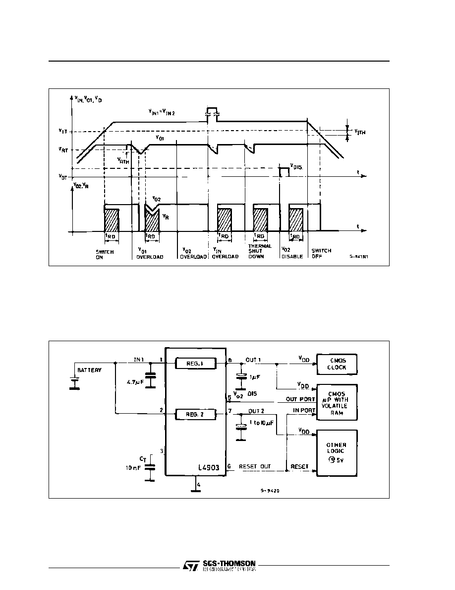
Figure 2
APPLICATION SUGGESTION
Figure 3 illustrates how the L4903's disable input
may be used in a CMOS
µ
Computer application.
The V
01
regulator (low consumption) supply perma-
nently a CMOS time of day clock and a CMOS
computer chip with volatile memory. V
02
output,
supplying non-essential circuits, is turned OFF un-
der control of a
µ
P unit.
Configurations of this type are used in products
where the OFF switch is part of a keyboard
scanned by a micro which operates continuously
even in the OFF state.
Figure 3
L4903
5/8
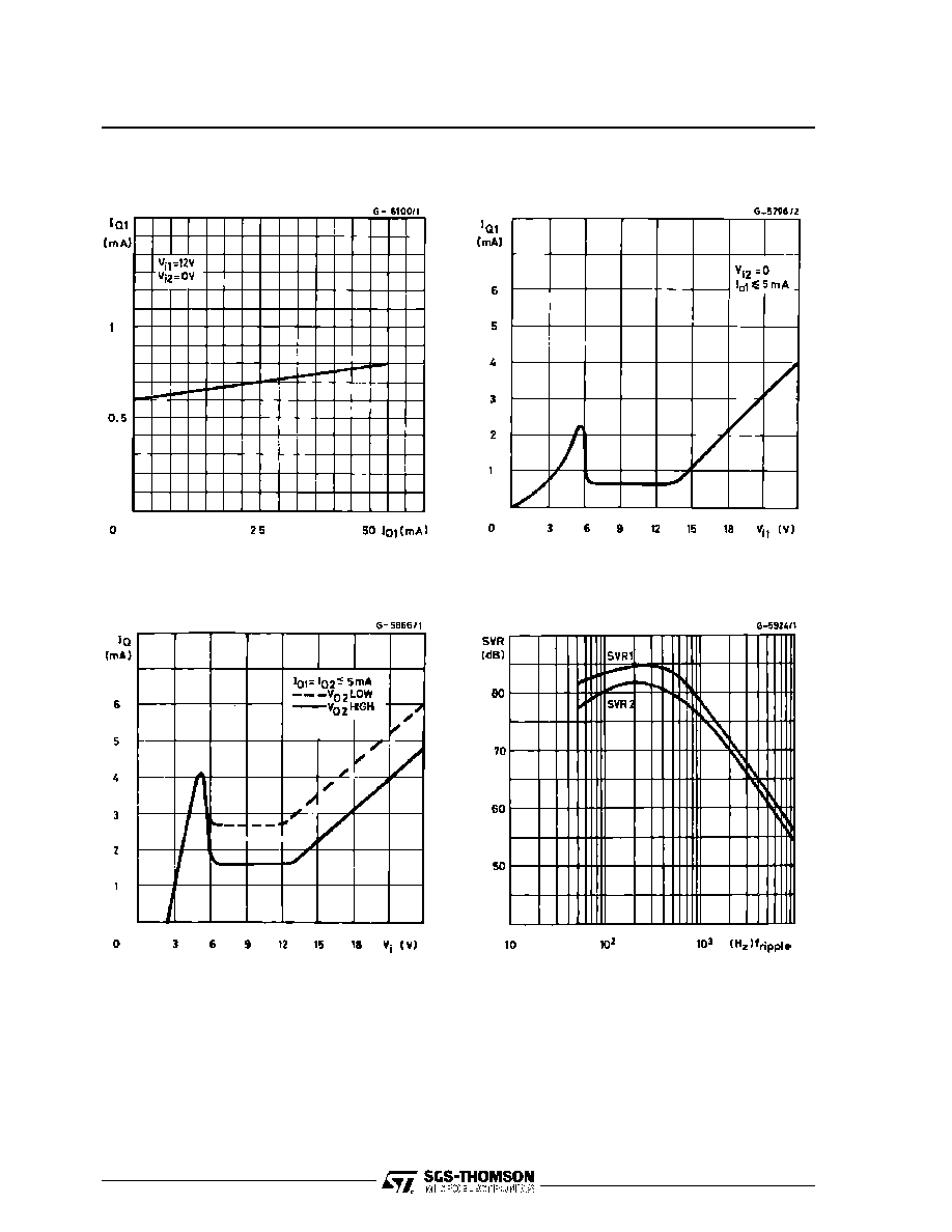
Figure 4 :
Quiescent Current (reg. 1) versus
Output Current
Figure 5 :
Quiescent Current (reg. 1 versus
Input Voltage
Figure 6 :
Total Quiescent Current versus
Input Voltage
Figure 7 :
Supply Voltage Rejection
Regulators 1 and 2 versus Input
Ripple Frequence
L4903
6/8
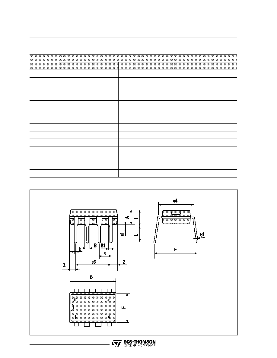
MINIDIP PACKAGE MECHANICAL DATA
DIM.
mm
inch
MIN.
TYP.
MAX.
MIN.
TYP.
MAX.
A
3.32
0.131
a1
0.51
0.020
B
1.15
1.65
0.045
0.065
b
0.356
0.55
0.014
0.022
b1
0.204
0.304
0.008
0.012
D
10.92
0.430
E
7.95
9.75
0.313
0.384
e
2.54
0.100
e3
7.62
0.300
e4
7.62
0.300
F
6.6
0.260
I
5.08
0.200
L
3.18
3.81
0.125
0.150
Z
1.52
0.060
L4903
7/8

Information furnished is believed to be accurate and reliable. However, SGS-THOMSON Microelectronics assumes no responsibility for the
consequences of use of such information nor for any infringement of patents or other rights of third parties which may result from its use. No
license is granted by implication or otherwise under any patent or patent rights of SGS-THOMSON Microelectronics. Specifications mentioned
in this publication are subject to change without notice. This publication supersedes and replaces all information previously supplied.
SGS-THOMSON Microelectronics products are not authorized for use as critical components in life support devices or systems without express
written approval of SGS-THOMSON Microelectronics.
©
1994 SGS-THOMSON Microelectronics - All Rights Reserved
SGS-THOMSON Microelectronics GROUP OF COMPANIES
Australia - Brazil - France - Germany - Hong Kong - Italy - Japan - Korea - Malaysia - Malta - Morocco - The Netherlands - Singa-
pore - Spain - Sweden - Switzerland - Taiwan - Thaliand - United Kingdom - U.S.A.
L4903
8/8