 | –≠–ª–µ–∫—Ç—Ä–æ–Ω–Ω—ã–π –∫–æ–º–ø–æ–Ω–µ–Ω—Ç: L4909 | –°–∫–∞—á–∞—Ç—å:  PDF PDF  ZIP ZIP |
1/7
L4909
May 2000
s
3 OUTPUTS
- Vo1 : output voltage variable from 5 to 12 V;
limit current : 1.2 A.
- Vo2 : output voltage variable from 5 to 12 V;
limit current : 1.2 A.
- Vo3 : output voltage variable from 5 to 12 V;
limit current : 1.2 A.
s
ENABLE INPUT FOR EACH REGULATOR
s
FEEDBACK INPUT FOR EACH REGULATOR
s
SHORT CIRCUIT PROTECTION TO GROUND
s
OVERCURRENT WARNING
s
DRIVER FOR EXTERNAL SCR (CROWBAR
PROTECTION)
s
THERMAL SHUTDOWN
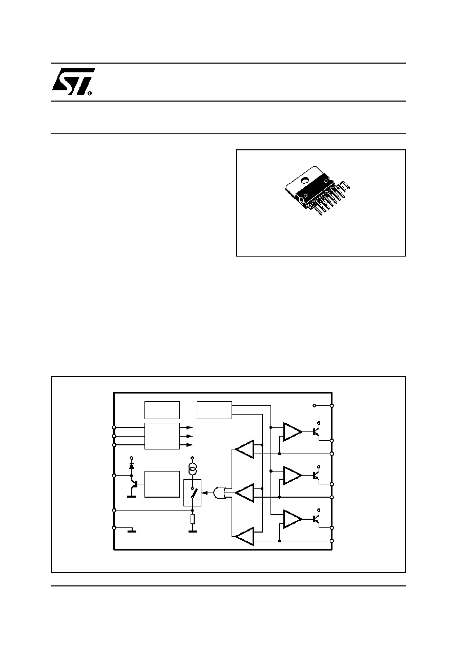
DESCRIPTION
It is a monolithic Multifunction Voltage Regulator; it
contains 3 regulators, (REG1, REG2, REG3) each
one with an enable input and a feedback input, to al-
low the voltage setting via external resistive divider.
Each regulator is current limited and furthermore an
OR-ed warning signal is output (open collector, ac-
tive low output) when the current in a regulator goes
above an over-current threshold (1 A typ for any reg-
ulator).
When one output voltage is higher than 20% typ of its
nominal value (for instance in case of input-to-output
short circuit), the crowbar output pin is activated, trig-
gering an external SCR (connected between input
and ground) that blows the input line fuse.
MULTIWATT 15
EXTERNALLY ADJUSTABLE MULTIFUNCTION REGULATOR
BLOCK DIAGRAM
THERMAL
SHUTDOWN
OVER
CURRENT
CHECK
ENABLE
CONTROL
REFERENCE
GENERATOR
REG1
REG1
6
7
9
4
5
8
10
11
15
14
3,13
REF
REF+20%
1
2
EN1
EN2
EN3
TRIG
OC
GND
V
O1
V
INA,
V
INB
FB1
V
O2
FB2
V
O3
FB3
D00AU1171
REG2
REG3
+
+
+
+
+
+
+
-
+
-
+
-
+
-
+
-
+
-
REG2
REG3
L4909
2/7
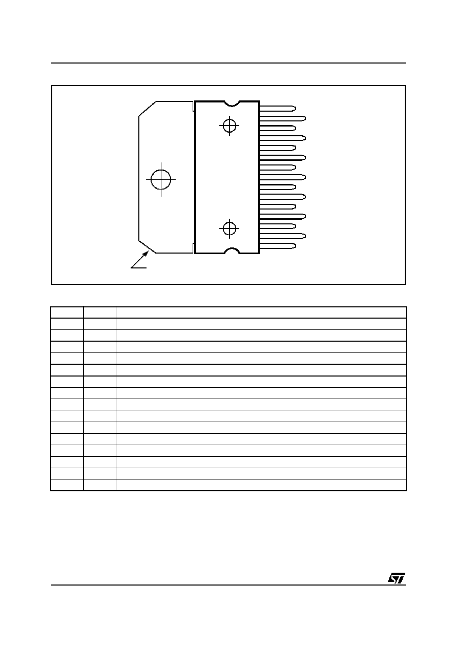
PIN CONNECTION
Table 1. Pin Description
No. Pin
Name
Function
1
FB1
REG1 feedback voltage input
2
Vo1
REG1 output voltage
3
VinA
Input DC supply voltage
4
TRIG
Trigger for external SCR (crowbar protection)
5
OC
Over current warning output
6
EN1
REG1 enable input
7
EN2
REG2 enable input
8
GND
Analog ground
9
EN3
REG3 enable input
10
FB3
REG3 feedback voltage input
11
Vo3
REG3 output voltage
12
N.C.
Not Connected
13
VinB
Input DC supply voltage
14
Vo2
REG2 output voltage
15
FB2
REG2 feedback voltage input
1
2
3
4
5
6
7
9
10
11
8
V
O3
FB3
EN3
GND
EN2
EN1
OC
TRIG
V
INA
V
O1
FB1
TAB CONNECTED TO PIN 8
13
14
15
12
FB2
V
O2
V
INB
N.C.
D00AU1153
3/7
L4909
ABSOLUTE MAXIMUM RATINGS
THERMAL DATA
ELECTRICAL CHARACTERISTICS (C
out
= 100nF; V
in
-V
o
= 5V; I
o
= 10mA; T
case
= 25
∞
C unless otherwise
specified
Symbol
Parameter
Value
Unit
Vin
VinA,VinB input DC supply voltage
40
V
Io
Vo1, Vo2, Vo3 output currents
internally limited
Voc
OC output voltage
min (15, Vin)
V
VENx
ENx input voltage
15
V
Top
Operating temperature range
0 to 70
o
C
Tstg
Storage temperature
- 40 to 150
o
C
Symbol
Parameter
Value
Unit
R
TH j-case
Thermal Resistance Junction to Case
1.8
∞
C/W
Symbol
Parameter
Test Condition
Min.
Typ.
Max.
Unit
Vo1
REG1 output voltage range
5
12
V
V(FB1)
REG1 feedback voltage
EN1=ON;
1.22
1.27
1.32
V
Ilim1
REG1 output current limit
EN1=ON; Vin-Vo1<12V
1.20
1.70
A
line regulation
Io1=10mA; Vin-Vo1=3 to 25 V
Io1=10mA; Vin-Vo1=3 to 12 V
0.6
0.1
2
%
load regulation
Io1=10 mA to 1.2A
Io1=10 mA to 0.5A
0.5
0.1
2
%
Vd1
REG1 drop out
Io1=500mA
2.20
V
SVR1
REG1 supply voltage rejec.
freq=120 Hz to 1KHz
60
dB
Vo2
REG2 output voltage range
5
12
V
V(FB2)
REG2 feedback voltage
EN2 = ON;
1.22
1.27
1.32
V
Ilim2
REG2 output current limit
EN2=ON; Vin-Vo2<12V
1.20
1.70
A
line regulation
Io2=10mA;Vin-Vo2=3 to 25 V
Io2=10mA;Vin-Vo2=3 to 12 V
0.6
0.1
2
%
load regulation
Io2=10 mA to 1.2A
Io2=10 mA to 0.5A
0.5
0.1
2
%
Vd2
REG2 drop out
Io2=500mA
2.2
V
V
o1
V
o1
-------------
V
o1
V
o1
-------------
V
o2
V
o2
-------------
V
o2
V
o2
-------------

L4909
4/7
SVR2
REG2 supply voltage rejec.
freq=120 Hz to 1KHz
60
dB
Vo3
REG3 output voltage range
5
12
V
V(FB3)
REG3 feedback voltage
EN3=ON;
1.22
1.27
1.32
V
Ilim3
REG3 output current limit
EN3=ON; Vin-Vo3<12V
1.20
1.70
A
line regulation
Io3=10mA; Vin-Vo3=3 to 25 V
Io3=10mA; Vin-Vo3=3 to 12 V
0.6
0.1
2
%
load regulation
Io3=10 mA to 1.2A
Io3=10 mA to 0.5A
0.5
0.1
2
%
Vd3
REG3 drop out
Io3=500mA
2.20
V
SVR3
REG3 supply voltage rejec.
freq=120 Hz to 1KHz
60
dB
ENx
enable input voltage
(active high)
STAND_BY
ON
3.5
0.8
V
V
Istby
current consumption in stand_by
EN1=EN2=EN3
0.5 V
20
µ
A
ITRIG
current at TRIG output
SCR trigger circuit in ON state;
V(TRIG) = 2V
25
mA
ZTRIG
TRIG to GND impedance
SCR trigger circuit in OFF state
0.2
K
V(FB)_TR
FBx voltage for trigger SCR on
any regulator
1.52
V
I(FB)
Feedback's input current
any regulator
2
µ
A
I(EN)
EN's input current
V(EN) = 5V
160
µ
A
Ion
current consumption in ON state
(current in the exter nal feedback resistors not
included)
one regulator ON; Vo = 12V
two regulators ON; Vo = 12V
three regulators ON; Vo = 12V
11
20
29
mA
V_OC_L
current_warning output
voltage
warning conditions
Isink < 3 mA
0.40
V
I_OC_H
current_warning leakage
no warning conditions
V(OC) = 15V
1
µ
A
I_oc/Ilim
warning threshold current / limit
current
any regulator
Vin - Vout <12V
0.6
Symbol
Parameter
Test Condition
Min.
Typ.
Max.
Unit
V
o3
V
o3
-------------
V
o3
V
o3
-------------
ELECTRICAL CHARACTERISTCS (continued)

5/7
L4909
The current protection is a function of the Vce, i.e. the drop between input and output voltages (Vin-Vo). The
shape of that relationship is shown in following figure 1.
Figure 1.
Figure 2. REGULATOR TYPICAL APPLICATION
(*)EN1
2
14
11
1
15
12
V
INA
V
INB
(*)EN2
(*)EN3
4.7K
PULL-UP
RESISTOR
100
µ
F
R
B3
R
B2
R
B1
R
A3
R
A2
R
A1
+5V
ULTRAFAST FUSE
FROM
RECTIFIER
330nF
100nF
SCR
OC
FB3
FB2
FB1
V
O3
V
O2
6
3
8
13
7
9
5
4
V
O1
TRIG
GND
100
µ
F
100nF
100
µ
F
100nF
D00AU1154
(*) It is possible to enable the regulators connecting the ENx pins to Vin through a 25K
Suggested value for R
Ax
is 1.2K
The value of R
Bx
must be choosen, depending on the desired output voltage V
ox?
following the formula:
R
Bx
= R
Ax
V
ox
1.27
-1