 | –≠–ª–µ–∫—Ç—Ä–æ–Ω–Ω—ã–π –∫–æ–º–ø–æ–Ω–µ–Ω—Ç: L4925N | –°–∫–∞—á–∞—Ç—å:  PDF PDF  ZIP ZIP |
L4925
VERY LOW DROP VOLTAGE REGULATOR
OPERATING DC SUPPLY VOLTAGE RANGE
6V TO 28V
TRANSIENT SUPPLY VOLTAGE UP TO 40V
EXTREMELY LOW QUIESCENT CURRENT
HIGH PRECISION OUTPUT VOLTAGE
OUTPUT CURRENT CAPABILITY UP TO
500mA
VERY LOW DROPOUT VOLTAGE LESS
THAN 0.6V
RESET CIRCUIT SENSING THE OUTPUT
VOLTAGE
PROGRAMMABLE RESET PULSE DELAY
WITH EXTERNAL CAPACITOR
THERMAL SHUTDOWN AND SHORT CIR-
CUIT PROTECTIONS
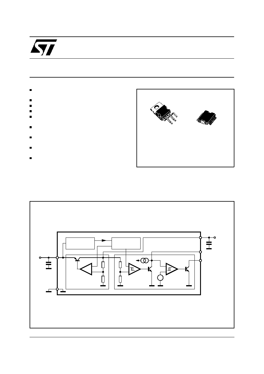
DESCRIPTION
The L4925 is a monolithic integrated 5V voltage
regulator with a very low dropout output and addi-
tional functions such as power-on reset and pro-
grammable reset delay time. It is designed for
supplying microcomputer controlled systems es-
pecially in automotive applications.
This is advanced information on a new product now in development or undergoing evaluation. Details are subject to change without notice.
October 2003
Æ
+
-
PREREGULATOR
5V
VREF
1.23V
Vz
Vz
2
µ
=
V
S
GND
2V
RESET
REG
L4925N
V
O
CT
RES
D95AT151
C
S
BLOCK DIAGRAM
ORDERING NUMBERS: L4925 (Pentawatt)
L4925PD (PowerSO20)
Pentawatt
PowerSO20
1/8
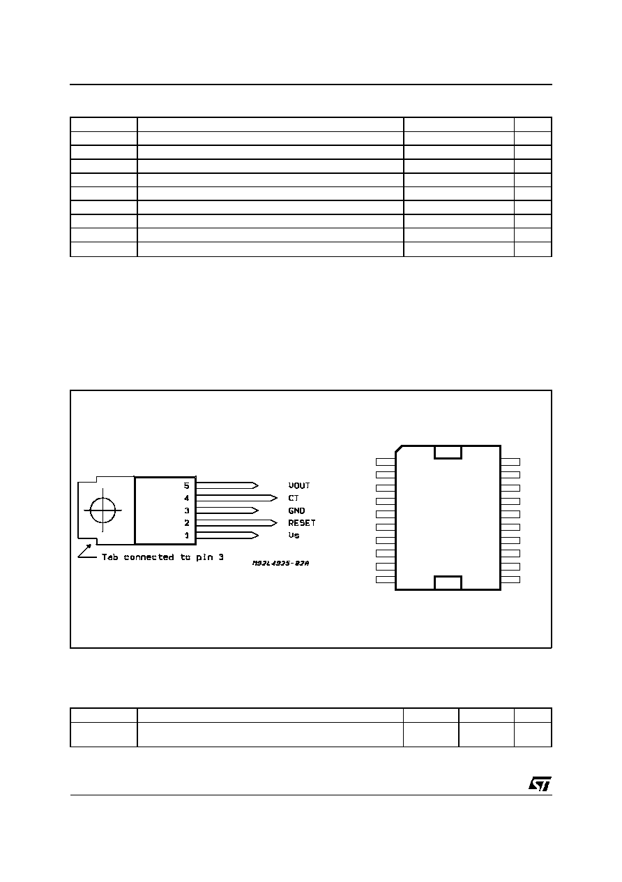
CONNECTION DIAGRAM
ABSOLUTE MAXIMUM RATINGS
Symbol
Parameter
Value
Unit
V
SDC
DC Operating Supply Voltage
28
V
V
STR
Transient Supply Voltage (t < 1s)
40
V
I
O
Output Current
internally limited
V
O
Output Voltage
20
V
V
RES
Output Voltage
20
V
I
RES
Output Current
5
mA
T
stg
Storage Temperature
-55 to 150
∞
C
T
j
Operating Junction Temperature
-40 to 150
∞
C
T
j-SD
Thermal Shutdown-Junction Temperature
165
∞
C
NOTE:
The circuit is ESD protected according to MIL-STD-883C. According to ISO/DIS 7637 the transients must be clamped with external circuitry
(see Application Circuit).
THERMAL DATA
Symbol
Parameter
Pentawatt
PSO 20
Unit
R
th j-amb
R
th j-case
Thermal resistance junction to ambient max.
Thermal resistance junction to case max.
20 to 60
3.5
15 to 60
3.5
∞
C/W
∞
C/W
N.C.
N.C.
N.C.
V
S
V
S
N.C.
N.C.
RES
N.C.
N.C.
GND
10
8
9
7
6
5
4
3
2
13
14
15
16
17
19
18
20
12
1
11
N.C.
D95AT152
N.C.
CT
V
OUT
N.C.
V
OUT
N.C.
N.C.
N.C.
L4925
2/8

ELECTRICAL CHARACTERISTICS (V
S
=14V T
j
=≠40 to 125
∞
C unless otherwise specified;
Symbol
Parameter
Test Condition
Min.
Typ.
Max.
Unit
V
O
Output Voltage
V
I
= 6 to 28V; I
O
= 1 to 500mA
4.90
5
5.10
V
V
O
Output Voltage
V
I
= 35V; T <1s;
I
O
= 1 to 500mA
5.50
V
V
DP
Dropout Voltage
I
O
= 100mA
I
O
= 500mA
0.2
0.3
0.3
0.6
V
V
V
IO
Input to Output Voltage
Difference in Undervoltage
Condition
V
I
= 4V; I
O
= 100mA
0.5
V
V
OL
Line Regulation
V
I
= 6 to 28V; I
O
= 1 to 1mA
10
mV
V
OLO
Load Regulation
I
O
= 1 to 500mA
50
mV
I
LIM
Current Limit
V
O
= 4.5V
;
V
O
= 0; Foldback characteristic
550
1000
250
1500
mA
mA
I
QSE
Quiescent Current
I
O
= 0.3mA
190
360
µ
A
I
Q
Quiescent Current
I
O
= 500mA
20
mA
RESET
Symbol
Parameter
Test Condition
Min.
Typ.
Max.
Unit
V
RT
Reset Threshold Voltage
4.5
5.2
V
V
RTH
Reset Threshold
50
100
200
mV
t
RD
Reset Pulse Delay
C
T
= 100nF; t
R
> 100
µ
s
60
100
140
ms
t
RR
Reset Reaction Time
C
T
= 100nF;
5
30
µ
s
V
RL
Reset Output LOW Voltage
R
RES
= 10K
to V
O
; V
S
=> 3V
0.4
V
I
RH
Reset Output HIGH Leakage
Current
V
RES
= 5V
1
µ
A
V
CTth
Delay Comparator Threshold
2
V
V
CTth hy
Delay Comparator Threshold
Hysteresis
200
mV
+
-
PREREGULATOR
5V
VREF
1.23V
Vz
Vz
2
µ
=
V
S
GND
2V
RESET
REG
L4925N
Vo
CT
RES
D95AT153
VBAT
C
S
Co
Vout
RES
APPLICATION CIRCUIT DIAGRAM
For stability: C
S
> 1
µ
F; C
O
> 10
µ
F;ESR < 2.5
at 10 KHz
Recommended for application: C
S
=C
O
= 10
µ
F to 100
µ
F
L4925
3/8
APPLICATION NOTE
SUPPLY VOLTAGE TRANSIENTS
High supply voltage transients can cause a reset
output signal disturbation.
For supply voltage greater than 8V the circuit
shows a high immunity of the reset output against
supply transients of more than 100V/
µ
s.
For supply voltage lower than 8V, supply tran-
sients of more than 0.4V/
µ
s. can cause a reset
signal disturbation.
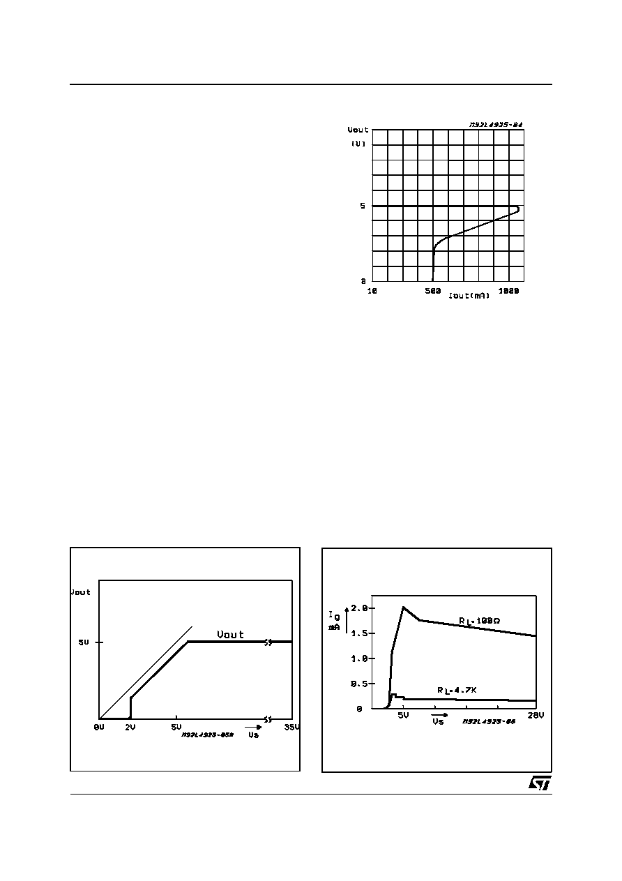
Foldback Characteristics Of Vo
FUNCTIONAL DESCRIPTION
The L4925 is a monolithic integrated voltage
regulator, based on the STM modular voltage
regulator approach. Several outstanding features
and auxiliary functions are implemented to meet
the requirements of supplying microprocessor
systems in automotive applications.
Nevetrheless, it is suitable also in other applica-
tions where the present functions are required.
The modular approach of this device allows to get
easily also other features and functions when re-
quired.
VOLTAGE REGULATOR
The voltage regulator uses an Isolated Collector
Vertical PNP transistor as a regulating element.
With this structure very low dropout voltage at
currents up to 500mA is obtained.
The dropout operation of the standby regulator is
maintained down to 3V input supply voltage. The
output voltage is regulated up to the transient in-
put supply voltage of 35V. With this feature no
functional interruption due to overvoltage pulses
is generated.
The typical curve showing the standby output
voltage as a function of the input supply voltage is
shown in fig. 1.
The current consumption of the device (quiescent
current) is less than 250
µ
A.
To reduce the quiescent current peak in the un-
dervoltage region and to improve the transient re-
sponse in this region, the dropout voltage is con-
trolled.
The quiescent current as a function of the supply
input voltage is shown in fig. 2.
Figure 1: Output Voltage vs. Input Voltage
Figure 2: Quiescent Current vs. Supply Voltage
L4925
4/8

RESET CIRCUIT
The block circuit diagram of the reset circuit is
shown in Figure 3. The reset circuit supervises
the output voltage. The reset threshold of 4.5V is
defined with the internal reference voltage and
standby output divider.
The reset pulse delay time t
RD
, is defined with the
charge time of an external capacitor C
T
:
t
RD
=
C
T
x 2V
2
µ
A
The reaction time of the reset circuit originates
from the discharge time limitation of the reset ca-
pacitor C
T
and it is proportional to the value of C
T
.
The reaction time of the reset circuit increases the
noise immunity.Standby output voltage drops be-
low the reset threshold only a bit longer than the
reaction time results in a shorter reset delay time.
The nominal reset delay time will be generated for
standby output voltage drops longer than approxi-
mately 50
µ
s. The typical reset output waveforms
are shown in Figure 4.
Figure 3
Figure 4
L4925
5/8
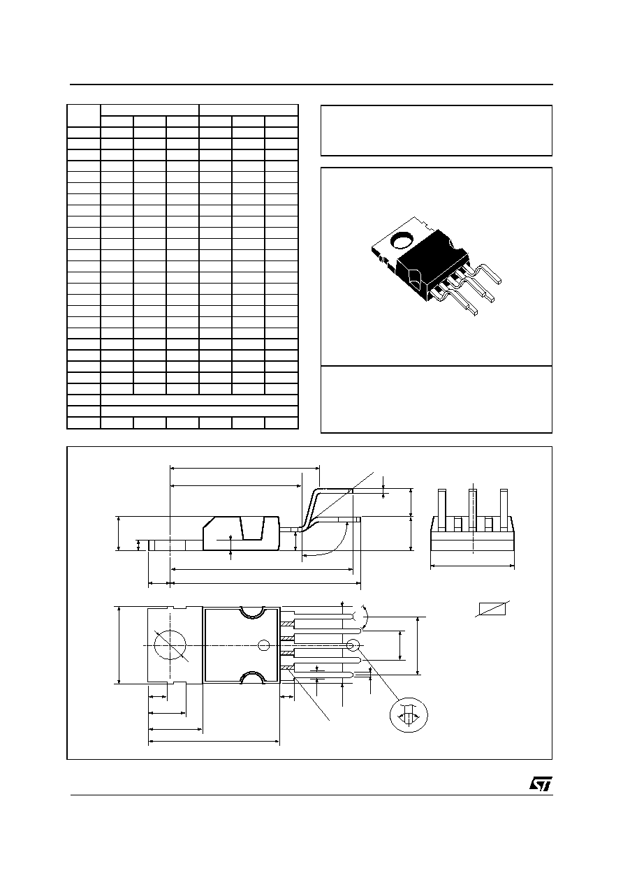
Weight: 2.00gr
Pentawatt V
DIM.
mm
inch
MIN.
TYP.
MAX.
MIN.
TYP.
MAX.
A
4.8
0.189
C
1.37
0.054
D
2.4
2.8
0.094
0.110
D1
1.2
1.35
0.047
0.053
E
0.35
0.55
0.014
0.022
E1
0.76
1.19
0.030
0.047
F
0.8
1.05
0.031
0.041
F1
1.0
1.4
0.039
0.055
G
3.2
3.4
3.6
0.126
0.134
0.142
G1
6.6
6.8
7.0
0.260
0.268
0.276
H2
10.4
0.409
H3
10.05
10.4
0.396
0.409
L
17.55
17.85
18.15
0.691
0.703
0.715
L1
15.55
15.75
15.95
0.612
0.620
0.628
L2
21.2
21.4
21.6
0.831
0.843
0.850
L3
22.3
22.5
22.7
0.878
0.886
0.894
L4
1.29
0.051
L5
2.6
3.0
0.102
0.118
L6
15.1
15.8
0.594
0.622
L7
6.0
6.6
0.236
0.260
L9
2.1
2.7
0.008
0.106
L10
4.3
4.8
0.17
0.189
M
4.23
4.5
4.75
0.167
0.178
0.187
M1
3.75
4.0
4.25
0.148
0.157
0.167
V4
40∞ (typ.)
V5
90∞ (typ.)
Dia
3.65
3.85
0.144
0.152
L
L1
A
C
L5
D1
L2
L3
E
M1
M
D
H3
Dia.
L7
L9
L10
L6
F1
H2
F
G G1
E1
F
E
V4
RESIN BETWEEN
LEADS
H2
V5
V4
PENTVME
L4
0015981
OUTLINE AND
MECHANICAL DATA
L4925
6/8

OUTLINE AND
MECHANICAL DATA
e
a2
A
E
a1
PSO20MEC
DETAIL A
T
D
1
10
11
20
E1
E2
h x 45
DETAIL A
lead
slug
a3
S
Gage Plane
0.35
L
DETAIL B
R
DETAIL B
(COPLANARITY)
G
C
- C -
SEATING PLANE
e3
b
c
N
N
H
BOTTOM VIEW
E3
D1
DIM.
mm
inch
MIN.
TYP.
MAX.
MIN.
TYP.
MAX.
A
3.6
0.142
a1
0.1
0.3
0.004
0.012
a2
3.3
0.130
a3
0
0.1
0.000
0.004
b
0.4
0.53
0.016
0.021
c
0.23
0.32
0.009
0.013
D (1)
15.8
16
0.622
0.630
D1
9.4
9.8
0.370
0.386
E
13.9
14.5
0.547
0.570
e
1.27
0.050
e3
11.43
0.450
E1 (1)
10.9
11.1
0.429
0.437
E2
2.9
0.114
E3
5.8
6.2
0.228
0.244
G
0
0.1
0.000
0.004
H
15.5
15.9
0.610
0.626
h
1.1
0.043
L
0.8
1.1
0.031
0.043
N
8∞ (typ.)
S
8∞ (max.)
T
10
0.394
(1) "D and E1" do not include mold flash or protusions.
- Mold flash or protusions shall not exceed 0.15mm (0.006")
- Critical dimensions: "E", "G" and "a3".
PowerSO20
0056635
JEDEC MO-166
Weight:
1.9gr
L4925
7/8

Information furnished is believed to be accurate and reliable. However, STMicroelectronics assumes no responsibility for the consequences
of use of such information nor for any infringement of patents or other rights of third parties which may result from its use. No license is
granted by implication or otherwise under any patent or patent rights of STMicroelectronics. Specifications mentioned in this publication are
subject to change without notice. This publication supersedes and replaces all information previously supplied. STMicroelectronics products
are not authorized for use as critical components in life support devices or systems without express written approval of STMicroelectronics.
The ST logo is a registered trademark of STMicroelectronics.
All other names are the property of their respective owners
© 2003 STMicroelectronics - All rights reserved
STMicroelectronics GROUP OF COMPANIES
Australia ≠ Belgium - Brazil - Canada - China ≠ Czech Republic - Finland - France - Germany - Hong Kong - India - Israel - Italy - Japan -
Malaysia - Malta - Morocco - Singapore - Spain - Sweden - Switzerland - United Kingdom - United States
www.st.com
L4925
8/8