 | –≠–ª–µ–∫—Ç—Ä–æ–Ω–Ω—ã–π –∫–æ–º–ø–æ–Ω–µ–Ω—Ç: L4937NPD | –°–∫–∞—á–∞—Ç—å:  PDF PDF  ZIP ZIP |

This is advanced information on a new product now in development or undergoing evaluation. Details are subject to change without notice.
L4937NPD
June 2000
DUAL 5V MULTIFUNCTION VOLTAGE REGULATOR
Æ
.
STANDBYOUTPUT VOLTAGEPRECISION 5V
±
2%
.
OUTPUT 2 TRACKED TO THE STANDBY OUT-
PUT
.
OUTPUT
2
DISABLE
FUNCTION
FOR
STANDBY MODE
.
VERY LOW QUIESCENT CURRENT, LESS
THAN 260
µ
A, IN STANDBY MODE
.
OUTPUT CURRENTS : I
01
= 50mA, I
02
= 500mA
.
VERY LOW DROPOUT (max 0.4V/0.6V)
.
OPERATING TRANSIENT SUPPLY VOLTAGE
UP TO 40V
.
POWER-ON RESET CIRCUIT SENSING THE
STANDBY OUTPUT VOLTAGE
.
POWER-ON RESET DELAY PULSE DEFINED
BY THE EXTERNAL CAPACITOR
.
THERMAL SHUTDOWN AND SHORT CIRCUIT
PROTECTIONS
PowerSO20
ORDERING NUMBER: L4937NPD
DESCRIPTION
The L4937NPD is a monolithic integrated dual volt-
age regulators with two very low dropout outputs
andadditionalfunctionssuchas power-onresetand
input voltage sense. They are designed for supply-
ing microcomputer controlled systems specially in
automotive applications.
PIN CONNECTION (top view)
GND
N.C.
N.C.
V
S
V
S
N.C.
GND
CT
EN
N.C.
GND
10
8
9
7
6
5
4
3
2
13
14
15
16
17
19
18
20
12
1
11
GND
D95AT162A
N.C.
RESET
V
O1
GND
N.C.
V
O2
N.C.
GND
1/9
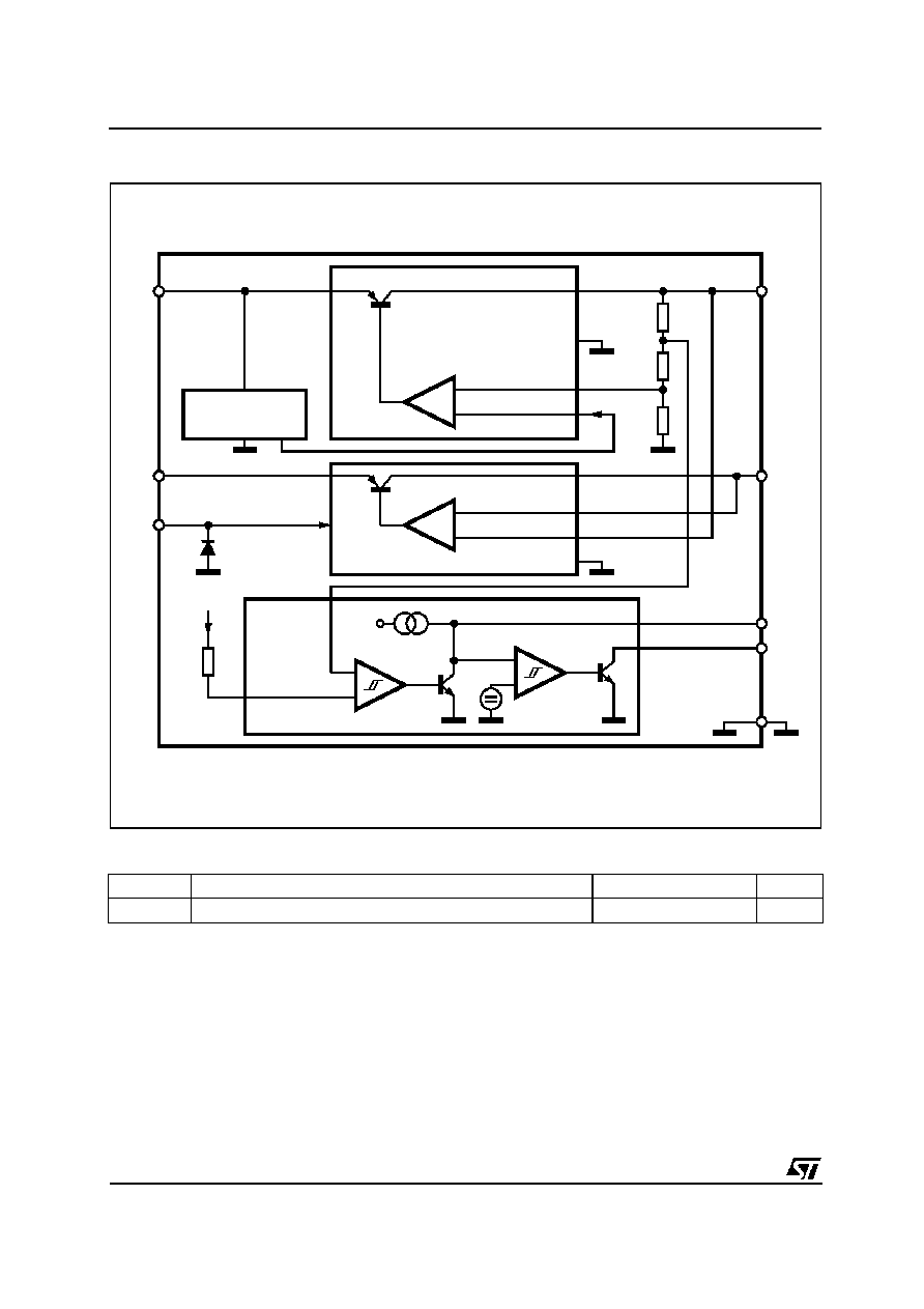
BLOCK DIAGRAM
REG1
1.23V
REFERENCE
REG2
RESET
2.0V
1.23V
V
S1
V
S2
EN
RES
CT
V
O2
V
O1
GND
D95AT163
2
µ
THERMAL DATA
Symbol
Parameter
Value
Unit
R
thj-case
Thermal Resistance Junction-Case
Max.
1.5
∞
C/W
L4937NPD
2/9
ABSOLUTE MAXIMUM RATINGS
Symbol
Parameter
Value
Unit
V
S
DC Supply Voltage
28
V
Transient Supply Voltage (T < 1s)
40
V
T
j
, T
stg
Junction and Storage Temperature Range
≠55 to 150
∞
C
I
EN
Enable Input Current (V
EN
0.3V)
±
1
mA
V
EN
Enable Input Voltage
V
S
V
RES
Reset Output Voltage
20
V
I
RES
Reset Output Current
5
mA
P
D
Power Dissipation
875
mW
REG1
1.23V
REFERENCE
REG2
RESET
2.0V
1.23V
V
S1
V
S2
EN
RES
CT
V
O2
V
O1
GND
D95AT164
C
S
CT
C
O1
2
µ
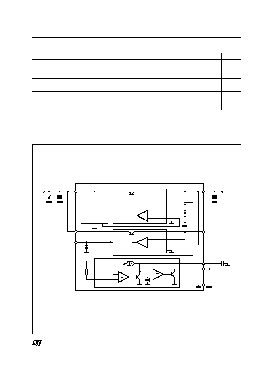
APPLICATION CIRCUIT
C
S
1
µ
F ; C
01
6
µ
F ; C
02
10
µ
F, ESR < 10
at 10KHz
Note : The circuit is ESD protected according to MIL≠STD≠883C.
L4937NPD
3/9

ELECTRICAL CHARACTERISTICS (V
S
= 14V; ≠40
∞
C
T
J
125
∞
C unless otherwise specified)
Symbol
Parameter
Test Conditions
Min.
Typ.
Max.
Unit
V
S
Operating Supply Voltage
25
V
V
O1
Standby Output Voltage
6V
V
S
25V
1mA
I
O1
50mA
4.90
5.00
5.10
V
V
O2
- V
O1
Output Voltage 2 Tracking Error
6V
V
S
25V
5mA
I
O2
500mA
Enable = LOW
≠25
+25
mV
V
DP1
Dropout Voltage 1
I
O1
= 10mA
I
O1
= 50mA
0.1
0.2
0.25
0.4
V
V
V
IO1
Input to Output Voltage
Difference in Undervoltage
Condition
Vs = 4V, I
O1
= 35mA
0.4
V
V
DP2
Dropout Voltage 2
IO1 = 100mA
I
O1
= 500mA
0.2
0.3
0.3
0.6
V
V
V
IO2
Input to Output Voltage
Difference in Undervoltage
Condition
Vs = 4.6V, I
O1
= 350mA
0.6
V
V
OL 1.2
Line Regulation
6V
V
S
25V
I
O1
= 1mA; I
O2
= 5mA
20
mV
V
OLO1
Load Regulation 1
1mA
I
O1
50mA
25
mV
V
OLO2
Load Regulation 2
5mA
I
O2
500mA
50
mV
I
LIM1
Current Limit 1
V
O1
= 4.5V
V
O1
= 0V (note 1)
55
25
100
50
200
100
mA
mA
I
LIM2
Current Limit 2
V
O2
= 0V
550
1000
1700
mA
I
QSB
Quiescent Current Standby Mode
(output 2 disabled)
I
O1
= 0.3mA; T
J
< 100
∞
C
V
EN
2.4V
V
S
= 14V
V
S
= 3.5V
210
340
290
850
µ
A
µ
A
I
Q
Quiescent Current
I
O1
= 50mA
I
O1
= 500mA
30
mA
ENABLE
V
ENL
Enable Input LOW Voltage
(output 2 active)
≠0.3
1.5
V
V
ENH
Enable Input HIGH Voltage
2.4
7
V
V
ENhyst
Enable Hysteresis
30
75
200
mV
I
EN
Enable Input Current
0V < V
EN
< 1.2V
2.5V < V
EN
< 7V
≠10
≠1
≠1.5
0
≠0.5
+1
µ
A
µ
A
L4937NPD
4/9
FUNCTIONAL DESCRIPTION
The L4937ND is based on the SGS-THOMSON Mi-
croelectronics modular voltage regulator approach.
Several out-standing features and auxiliary func-
tions are provided to meet the requirements of sup-
plying the microprocessor systems used in automo-
tive applications.
Furthermore the device is suitable also in other ap-
plications requiring two stabilized voltages.
The modular approach allows other features and
functions to be realized easily when required.
STANDBY REGULATOR
The standby regulator uses an Isolated Collector
Vertical PNP transistor as the regulating element.
This structure allows a very low dropout voltage at
currents up to 50mA. The dropout operation of the
standby regulator is maintained down to 2V input
supply voltage. The output voltage is regulated up
to the transientinput supplyvoltageof 40V.This fea-
ture avoids functional interruptions which could be
generated by overvoltage pulses.
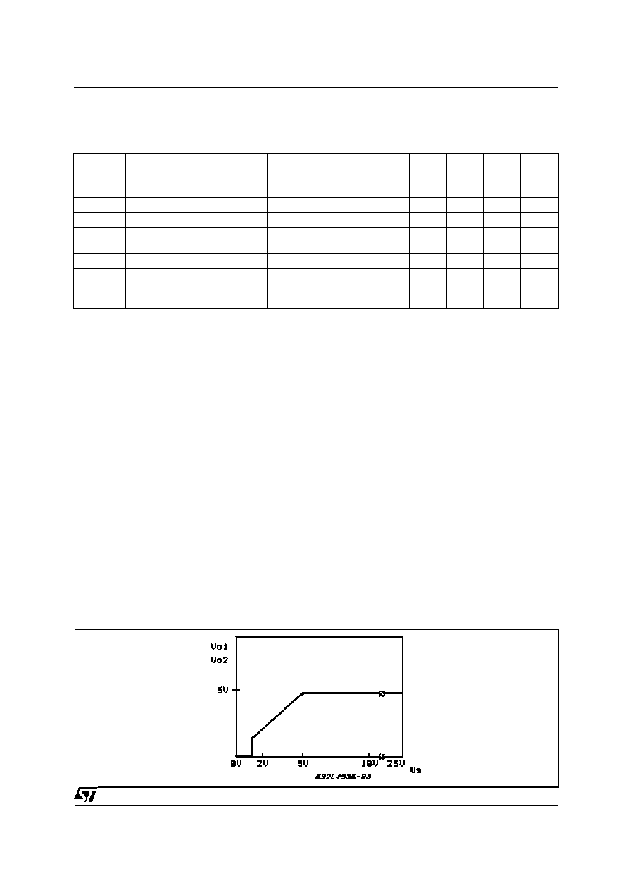
The typical curve of the standby output voltage as a
functionof the input supply voltage is shown in fig. 1.
The current consumption of the device (quiescent
current) is less than 260
µ
A when output 2 is dis-
abled (standby mode). The dropout voltage is con-
trolled to reduce the quiescent current peak in the
undervoltage region and to improve the transient
response in this region.
The quiescentcurrent is shown in fig. 2 as a function
of the supply input voltage 2.
OUTPUT 2 VOLTAGE
The output 2 regulator uses the same output struc-
ture as the standbyregulator, but rated for an output
current of 500mA.
The output 2 regulator works in tracking mode with
the standby output voltage as a reference voltage
when the output 2.
The output 2 regulator can be switched off via the
Enable input.
Note : 1: Foldback characteristic
ELECTRICAL CHARACTERISTICS (continued)
RESET
Symbol
Parameter
Test Conditions
Min.
Typ.
Max.
Unit
V
Rt
Reset Low Threshold Voltage
V
o1
-0.4
4.7
V
o1
-0.1
V
V
Rth
Reset Threshold Hysteresis
50
100
200
mV
t
RD
Reset Pulse Delay
C
T
= 100nF; t
R
> 100
µ
s
55
100
180
ms
t
RR
Reset Reaction Time
C
T
= 100nF
1
10
50
µ
s
V
RL
Reset Output LOW Voltage
R
RES
= 10K
to V
01
V
S
= 1.5V
0.4
V
I
LRES
Reset Output HIGH Leakage
V
RES
= 5V
1
µ
A
V
CTh
Delay Comparator Threshold
2.0
V
V
CTh, hyst
Delay Comparator Threshold
Hysteresis
100
mV
Figure 1 : Output Voltage vs. Input Voltage.
L4937NPD
5/9
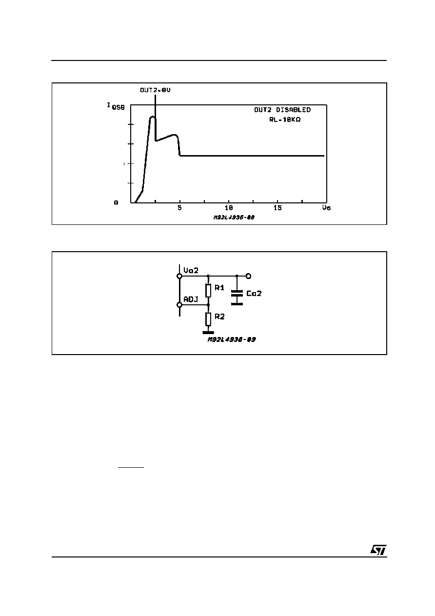
Figure 2 : Quiescent Current vs. Supply Voltage.
Figure 3 : Programmable Output 2 Voltage with External Resistors.
400
µ
200
µ
RESET CIRCUIT
The blockcircuit diagramof thereset circuit is shown
in fig.4. The reset circuit supervisesthe standbyout-
put voltage. The reset threshold of 4.7V is defined
by the internal reference voltage and the standby
output divider.
The reset pulse delay time t
RD
, is defined by the
charge time of an external capacitor C
T
:
C
T
x 2V
t
RD
=
2
µ
A
The reactiontime of the reset circuit dependson the
discharge time limitation of the reset capacitor C
T
and is proportional to the value of C
T
.
The reaction time of the reset circuit increases the
noise immunity. In fact,if the standbyoutputvoltage
drops below the reset threshold for a time shorter
than the reaction time t
RR
, no reset output variation
occurs. The nominal reset delay is generated for
standby output voltage drops longer than the time
necessary for the complete discharging of the ca-
pacitor C
T
. This time is typically equal to 50
µ
s if
C
T
= 100nF.The typical reset output waveforms are
shown in fig. 5.
L4937NPD
6/9

Figure 4 :Block Diagram of the Reset Circuit.
VINPUT
VOUT1
VOUT1
VRT +0.2V
VRT
1.5V
RESET
t
R
t
RD
t
RD
t
RR
D95AT216
Figure 5 : Typical Reset Output Waveforms.
L4937NPD
7/9
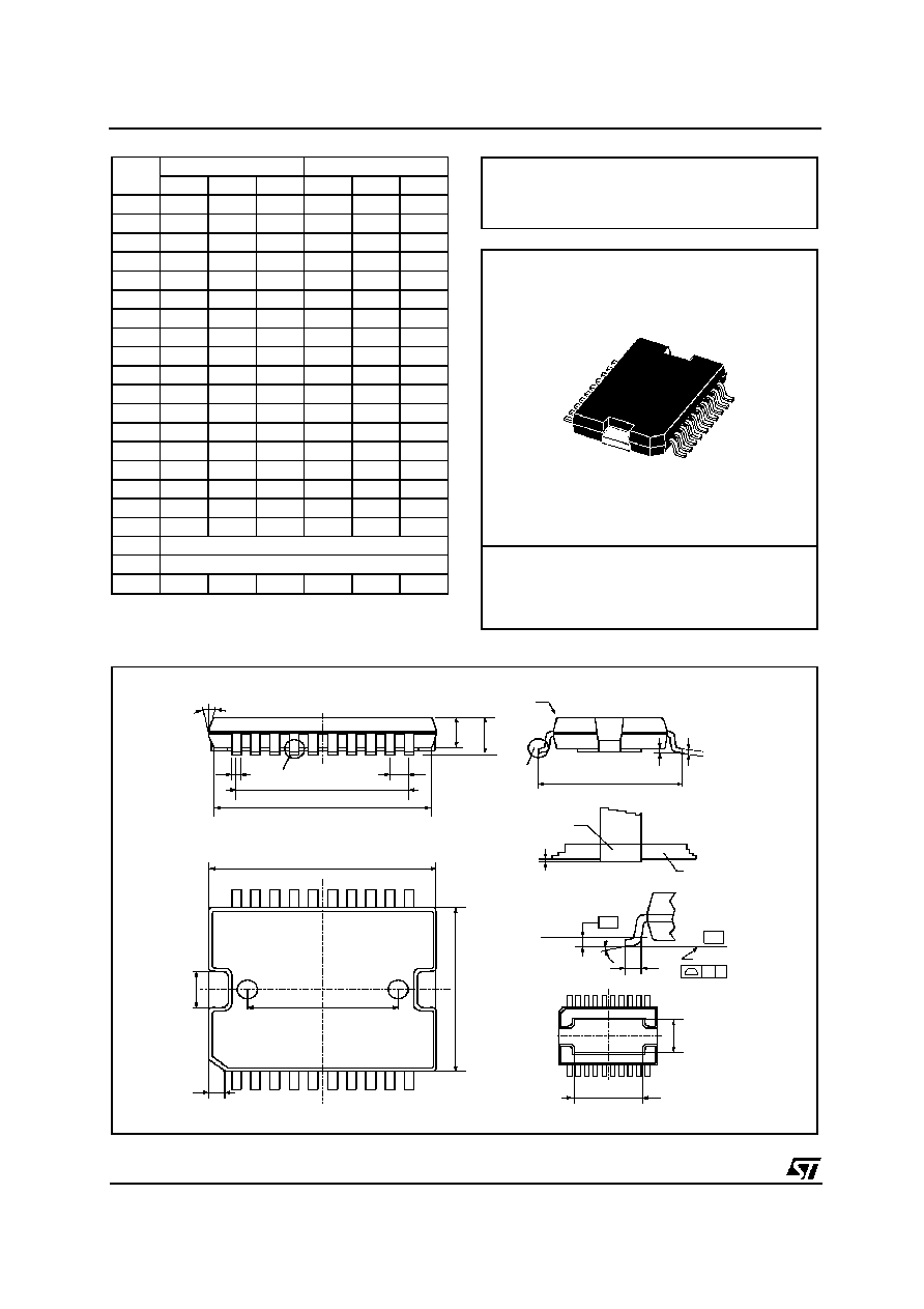
JEDEC MO-166
PowerSO20
e
a2
A
E
a1
PSO20MEC
DETAIL A
T
D
1
11
20
E1
E2
h x 45
DETAIL A
lead
slug
a3
S
Gage Plane
0.35
L
DETAIL B
R
DETAIL B
(COPLANARITY)
G
C
- C -
SEATING PLANE
e3
b
c
N
N
H
BOTTOM VIEW
E3
D1
DIM.
mm
inch
MIN.
TYP.
MAX.
MIN.
TYP.
MAX.
A
3.6
0.142
a1
0.1
0.3
0.004
0.012
a2
3.3
0.130
a3
0
0.1
0.000
0.004
b
0.4
0.53
0.016
0.021
c
0.23
0.32
0.009
0.013
D (1)
15.8
16
0.622
0.630
D1
9.4
9.8
0.370
0.386
E
13.9
14.5
0.547
0.570
e
1.27
0.050
e3
11.43
0.450
E1 (1)
10.9
11.1
0.429
0.437
E2
2.9
0.114
E3
5.8
6.2
0.228
0.244
G
0
0.1
0.000
0.004
H
15.5
15.9
0.610
0.626
h
1.1
0.043
L
0.8
1.1
0.031
0.043
N
10
∞
(max.)
S
T
10
0.394
(1) "D and F" do not include mold flash or protrusions.
- Mold flash or protrusions shall not exceed 0.15 mm (0.006").
- Critical dimensions: "E", "G" and "a3"
OUTLINE AND
MECHANICAL DATA
8
∞
(max.)
10
L4937NPD
8/9

Information furnished is believed to be accurate and reliable. However, STMicroelectronics assumes no responsibility for the conse-
quences of use of such information nor for any infringement of patents or other rights of third parties which may result from its use. No
license is granted by implication or otherwise under any patent or patent rights of STMicroelectronics. Specification mentioned in this
publication are subject to change without notice. This publication supersedes and replaces all information previously supplied. STMi-
croelectronics products are not authorized for use as critical components in life support devices or systems without express written
approval of STMicroelectronics.
The ST logo is a registered trademark of STMicroelectronics
©
2000 STMicroelectronics ≠ Printed in Italy ≠ All Rights Reserved
STMicroelectronics GROUP OF COMPANIES
Australia - Brazil - China - Finland - France - Germany - Hong Kong - India - Italy - Japan - Malaysia - Malta - Morocco -
Singapore - Spain - Sweden - Switzerland - United Kingdom - U.S.A.
http://www.st.com
L4937NPD
9/9