L4940 series
VERY LOW DROP 1.5 A REGULATORS
November 1999
s
PRECISE 5 V, 8.5 V, 10 V, 12 V OUTPUTS
s
LOW DROPOUT VOLTAGE (500 mV typ
at 1.5A)
s
VERY LOW QUIESCENT CURRENT
s
THERMAL SHUTDOWN
s
SHORT CIRCUIT PROTECTION
s
REVERSE POLARITY PROTECTION
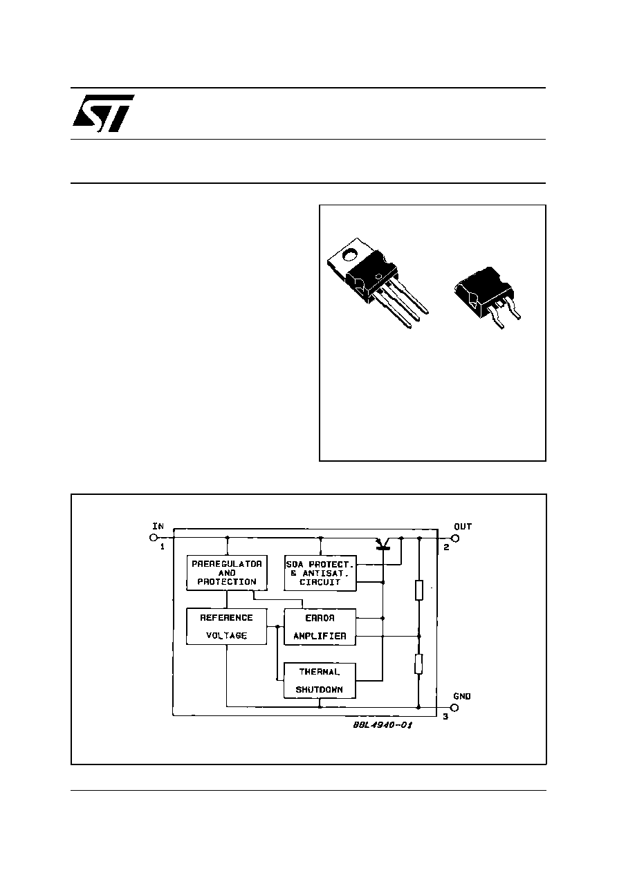
DESCRIPTION
The L4940 series of three terminal positive
regulators is available in TO-220 and D
2
PAK
package and with several fixed output voltages,
making it useful in a wide range of industrial and
consumer applications. Thanks to its very low
input/output voltage drop, these devices are
particularly
suitable
for
battery
powered
equipments,
reducing
consumption
and
prolonging battery life.
Each
type employs
internal current limiting, antisaturation circuit,
thermal shut-down and safe area protection.
BLOCK DIAGRAM
D
2
PAK
TO-263
TO-220
�
1/13
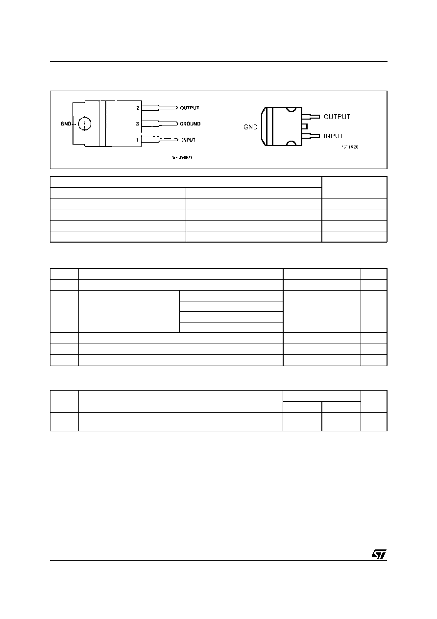
PIN CONNECTION AND ORDER CODES
ORDERING NUMBERS
OUTPUT VOLTAGE
TO-220
D
2
PAK
L4940V5
L4940D2T5
5V
L4940V85
L4940D2T85
8.5V
L4940V10
L4940D2T10
10V
L4940V12
L4940D2T12
12V
ABSOLUTE MAXIMUM RATING
Symbol
Description
Values
Unit
V
I
Forward Input Voltage
30
V
V
IR
Reverse Input Voltage
V
O
= 5 V
R
O
= 100
-15
V
V
O
= 8.5 V R
O
= 180
V
O
= 10 V
R
O
= 200
V
O
= 12 V
R
O
= 240
I
O
Output Current
I nternally Limited
P
tot
Power Dissipation
I nternally Limited
T
j
, T
st g
Junction and Storage Temperature
-40 to 150
o
C
THERMAL DATA
Symbol
Description
Value
Unit
TO-220
D
2
PAK
R
thj- ca s e
R
thj-a mb
Thermal Resistance Junction-case
Max
Thermal Resistance Junction-ambient
Max
3
50
3
62.5
o
C/W
o
C/W
L4940 series
2/13
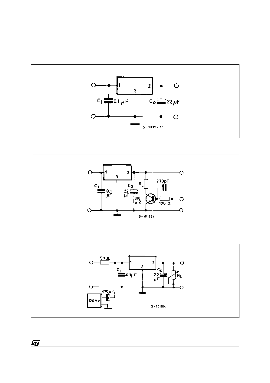
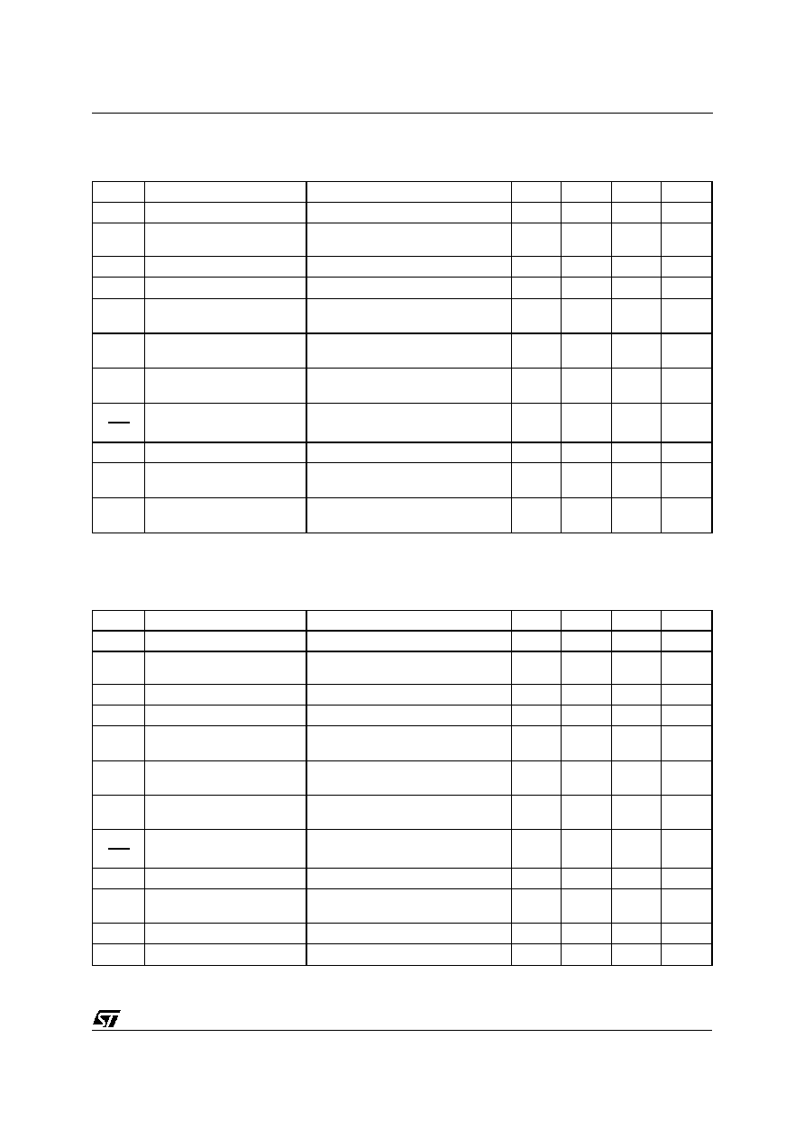
ELECTRICAL CHARACTERISTICS FOR L4940V85 (refer to the test circuits, T
j
= 25
o
C,
V
i
= 10.5V, C
i
= 0.1
�
F, C
o
= 22
�
F unless otherwise specified)
Symbol
Parameter
Test Conditions
Min.
Typ.
Max.
Unit
V
o
Output Voltage
I
o
= 500 mA
8.3
8.5
8.7
V
V
o
Output Voltage
I
o
= 5 mA to 1500 mA
V
i
= 10.2 to 16 V
8.15
8.5
8.85
V
V
i
Operating Input Voltage
I
o
= 5 mA
17
V
V
o
Line Regulation
I
o
= 5 mA
V
i
= 9.5 to 17 V
4
9
mV
V
o
Load Regulation
I
o
= 5 to 1500 mA
I
o
= 500 to 1000 mA
12
8
30
16
mV
I
Q
Quiescent Current
I
o
= 5 mA
I
o
= 1.5 A V
i
= 10.2 V
4
30
8
50
mA
I
Q
Quiescent Current Change
I
o
= 5 mA
I
o
= 1.5 A V
i
= 10.2 to 16 V
2.5
15
mA
V
o
T
Output Voltage Drift
0.8
mV/
o
C
SVR
Supply Voltage Rejection
I
o
= 1 A
f = 120 Hz
58
66
dB
V
d
Dropout Voltage
I
o
= 0.5 A
I
o
= 1.5 A
200
500
400
900
mV
I
s c
Short Circuit Current
V
i
= 14 V
V
i
= 10.2 V
2
2.2
2.7
2.9
A
ELECTRICAL CHARACTERISTICS FOR L4940V5 (refer to the test circuits, T
j
= 25
o
C,
V
i
= 7V, C
i
= 0.1
�
F, C
o
= 22
�
F unless otherwise specified)
Symbol
Parameter
Test Conditions
Min.
Typ.
Max.
Unit
V
o
Output Voltage
I
o
= 500 mA
4.9
5
5.1
V
V
o
Output Voltage
I
o
= 5 mA to 1500 mA
V
i
= 6.5 to 16 V
4.8
5
5.2
V
V
i
Operating Input Voltage
I
o
= 5 mA
17
V
V
o
Line Regulation
I
o
= 5 mA
V
i
= 6 to 17 V
4
10
mV
V
o
Load Regulation
I
o
= 5 to 1500 mA
I
o
= 500 to 1000 mA
8
5
25
15
mV
I
Q
Quiescent Current
I
o
= 5 mA
I
o
= 1.5 A V
i
= 6.5 V
5
30
8
50
mA
I
Q
Quiescent Current Change
I
o
= 5 mA
I
o
= 1.5 A V
i
= 6.5 to 16 V
3
15
mA
V
o
T
Output Voltage Drift
0.5
mV/
o
C
SVR
Supply Voltage Rejection
I
o
= 1 A
f = 120 Hz
58
68
dB
V
d
Dropout Voltage
I
o
= 0.5 A
I
o
= 1.5 A
200
500
400
900
mV
I
s c
Short Circuit Current
V
i
= 14 V
V
i
= 6.5 V
2
2.2
2.7
2.9
A
L4940 series
4/13
ELECTRICAL CHARACTERISTICS FOR L4940V10 (refer to the test circuits, T
j
= 25
o
C,
V
i
= 12V, C
i
= 0.1
�
F, C
o
= 22
�
F unless otherwise specified)
Symbol
Parameter
Test Conditions
Min.
Typ.
Max.
Unit
V
o
Output Voltage
I
o
= 500 mA
9.8
10
10.2
V
V
o
Output Voltage
I
o
= 5 mA to 1500 mA
V
i
= 11.7 to 16 V
9.6
10
10.4
V
V
i
Operating Input Voltage
I
o
= 5 mA
17
V
V
o
Line Regulation
I
o
= 5 mA
V
i
= 11 to 17 V
3
8
mV
V
o
Load Regulation
I
o
= 5 to 1500 mA
I
o
= 500 to 1000 mA
15
10
35
20
mV
I
Q
Quiescent Current
I
o
= 5 mA
I
o
= 1.5 A V
i
= 11.7 V
4
30
8
50
mA
I
Q
Quiescent Current Change
I
o
= 5 mA
I
o
= 1.5 A V
i
= 11.7 to 16 V
2
13
mA
V
o
T
Output Voltage Drift
1
mV/
o
C
SVR
Supply Voltage Rejection
I
o
= 1 A
f = 120 Hz
56
62
dB
V
d
Dropout Voltage
I
o
= 0.5 A
I
o
= 1.5 A
200
500
400
900
mV
I
s c
Short Circuit Current
V
i
= 14 V
V
i
= 11.7 V
2
2.2
2.7
2.9
A
A
ELECTRICAL CHARACTERISTICS FOR L4940V12 (refer to the test circuits, T
j
= 25
o
C,
V
i
= 14V, C
i
= 0.1
�
F, C
o
= 22
�
F unless otherwise specified)
Symbol
Parameter
Test Conditions
Min.
Typ.
Max.
Unit
V
o
Output Voltage
I
o
= 500 mA
11.75
12
12.25
V
V
o
Output Voltage
I
o
= 5 mA to 1500 mA
V
i
= 13.8 to 17 V
11.5
12
12.5
V
V
i
Operating Input Voltage
I
o
= 5 mA
17
V
V
o
Line Regulation
I
o
= 5 mA
V
i
= 13 to 17 V
3
7
mV
V
o
Load Regulation
I
o
= 5 to 1500 mA
I
o
= 500 to 1000 mA
15
10
35
25
mV
I
Q
Quiescent Current
I
o
= 5 mA
I
o
= 1.5 A V
i
= 13.8 V
4
30
8
50
mA
I
Q
Quiescent Current Change
I
o
= 5 mA
I
o
= 1.5 A V
i
= 13.8 to 16 V
1.5
10
mA
V
o
T
Output Voltage Drift
1.2
mV/
o
C
SVR
Supply Voltage Rejection
I
o
= 1 A
f = 120 Hz
55
61
dB
V
d
Dropout Voltage
I
o
= 0.5 A
I
o
= 1.5 A
200
500
400
900
mV
I
s c
Short Circuit Current
V
i
= 14 V
2
2.7
A
Z
o
Output Impedance
f = 1KHz
I
o
= 0.5A
40
m
L4940 series
5/13