 | –≠–ª–µ–∫—Ç—Ä–æ–Ω–Ω—ã–π –∫–æ–º–ø–æ–Ω–µ–Ω—Ç: L4946 | –°–∫–∞—á–∞—Ç—å:  PDF PDF  ZIP ZIP |
L4946
QUAD VOLTAGE REGULATOR WITH INHIBIT AND RESET
4 OUTPUTS: 10V (125mA); 8V (250mA); 5V
(200mA); 5V (100mA)
10V AND 5V (100mA) OUTPUT ARE LOW
DROP
5V (100mA) ST-BY OUTPUT VOLTAGE
EARLY WARNING OUTPUT FOR SUPPLY
UNDERVOLTAGE (LVW)
THERMAL
SHUTDOWN
AND
CURRENT
LIMITATION (FOLDBACK)
REVERSE BATTERY AND LOAD DUMP
PROTECTION
INHIBIT (ON/OFF) AND RESET FUNCTIONS
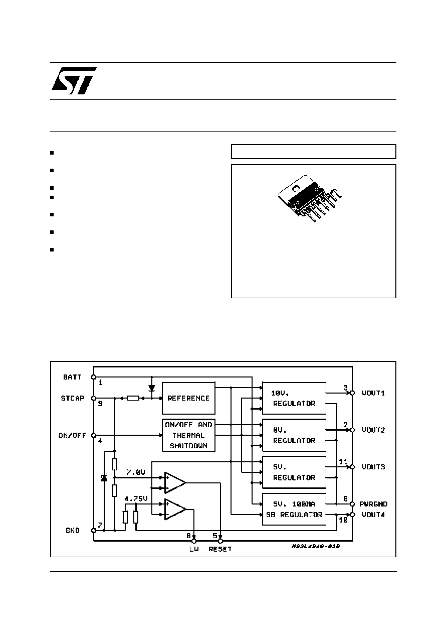
DESCRIPTION
The L4946 is a quad output low drop voltage
regulator. The four outputs are a low drop 10V at
125mA (V
O1
), a 8V at 250mA (V
O2
), a 5V at
200mA (V
O3
) and a low drop 5V st-by line at
100mA (V
O4
).
The IC includes a monitoring circuit to warn if a
low voltage or no voltage condition is occurring.
V
O1,2,3
are off during st-by mode.
The STCAP pin allows the battery voltage to de-
cay slowly giving the
µ
P time to store data. This
IC is designed for supplying microcomputer con-
trolled systems specially in automotive applica-
tions.
June 2000
Æ
BLOCK DIAGRAM
Multiwatt 11
ORDERING NUMBER: L4946
MULTIPOWER BCD TECHNOLOGY
L4946
125mA
250mA
200mA
1/9

OPERATING CONDITION
Symbol
Parameter
Value
Unit
V
S
Supply Voltage
-13.5 to 26.5
V
I
L
Load Current I
O1
I
O2
I
O3
I
O4
300
400
600
100
mA
mA
mA
mA
THERMAL DATA
Symbol
Parameter
Value
Unit
R
th j-case
Thermal Resistance Junction-case
max
2
∞
C/W
PIN CONNECTION
ABSOLUTE MAXIMUM RATINGS
Symbol
Parameter
Value
Unit
V
S
Supply Voltage
-35 to 60
V
V
I
Input Voltage (ON/OFF)
0 to 5
V
V
O
Output Voltage (LVW, Reset)
0 to 5
V
T
stg
Storage Temperature Range
-65 to 150
∞
C
T
j
Junction Temperature Range
max 150
∞
C
Load Dump (5ms rise, 115ms decay)
60
V
APPLICATION CIRCUIT
L4946
0.1
uF
L4946
2/9

ELECTRICAL CHARACTERISTICS (V
S
= 10.5 to 16V; I
O1
= 6mA, I
O2
= 8mA, I
O3
= 4mA; I
O4
= 0.4mA;
C
O
= 10
µ
F max; T
amb
= -40 to 85
∞
C, unless otherwise specified.)
Symbol
Parameter
Test Condition
Min.
Typ.
Max.
Unit
V
O1
Output Voltage
I
O1
= 125mA;
T
amb
= 25
∞
C;
11V < V
S
< 16V
all temps
9.7
9.5
10
10
10.3
10.5
V
V
V
O1
Load Regulation
I
O1
= 5 to 125mA
150
mV
I
Q
Quiescent Current (
I
S
)
V
S
= 14V; I
O1
= 5mA;
V
S
=14V ; I
O1
= 125mA;
10
18
mA
mA
V
S
-V
O1
Dropout Voltage
I
O1
= 125mA
T
amb
= 25
∞
C
all temps
400
600
mV
mV
L
Current Limit (Foldback) note1
V
O1
= 0V
150
300
mA
V
O1
Max Bat.Trans.
R
O
= 100
Ramp V
S
from 14 to 60V in 3-5ms
11
V
Hold V
S
at 60V for 10ms
Ramp V
S
from60 to 14V in 3-5ms;
T
amb
= 25
∞
C;
all temps
9.7
9.5
10
10
2
10.3
10.5
V
V
V
V
O1
Rev. Voltage Trans.
V
S
= -35V; t
1ms; R
O
= 100
Check V
O1
,
T
amb
= 25
∞
C;
all temps
9.7
9.5
10
10
10.3
10.5
V
V
V
O1
Rev. Voltage .
V
S
= -15V; R
O
= 100
-0.4
1
V
Ripple rejection
(by design only)
f
O
= 120-10KHz; 1V
pp
AC ; V
S
=14V
I
O1
= 90mA; I
O2
= 125mA
;
I
O3
= 75mA; I
O4
= 50mA;
50
dB
f
O
= 20-20KHz; 1V
pp
AC ; V
S
=14V
I
O1
= 90mA; I
O2
= 125mA
;
I
O3
= 75mA; I
O4
= 50mA;
50
dB
V
O1
Line Regulation
V
O1
across V
S
range
V
S
= 11V to 26V
50
mV
V
O2
Output Voltage
I
O2
= 250mA; T
amb
= 25
∞
C;
all temps
7.75
7.60
8
8
8.25
8.40
V
V
V
O2
Load Regulation
I
O2
= 5 to 250mA
150
mV
I
Q
Quiescent Current (
I
S
)
V
S
= 14V; I
O2
= 5mA;
V
S
= 14V; I
O2
= 250mA;
10
35
mA
mA
V
S
-V
O2
Dropout Voltage
I
O2
= 250mA
T
amb
= 25
∞
C
all temps
400
600
mV
mV
L
Current Limit (note1)
V
O2
= 0V
300
600
mA
V
O2
Max Bat.Trans.
R
O
= 100
Ramp V
S
from 14 to 60V in 3-5ms
9
V
Hold V
S
at 60V for 10ms
Ramp V
S
from60 to 14V in 3-5ms;
T
amb
= 25
∞
C;
all temps
7.85
7.60
8
8
2
8.15
8.20
V
V
V
V
O2
Rev. Voltage Trans.
V
S
= -35V; t < 1ms; R
O
= 100
Check V
O2
, standard
T
amb
= 25
∞
C
all temps
7.85
7.80
8
8
8.15
8.20
V
V
V
O2
Rev. Voltage .
V
S
= -15V; t = 30s; R
O
= 100
-0.4
1
V
L4946
3/9
ELECTRICAL CHARACTERISTICS (continued)
Symbol
Parameter
Test Condition
Min.
Typ.
Max.
Unit
Ripple rejection
f
O
= 120-10KHz; 1V
pp
AC ; V
S
=14V
I
O1
= 90mA; I
O2
= 125mA
;
I
O3
= 75mA; I
O4
= 50mA;
50
dB
f
O
= 20-20KHz; 1V
pp
AC ; V
S
=14V
I
O1
= 90mA; I
O2
= 125mA
;
I
O3
= 75mA; I
O4
= 50mA;
50
dB
V
O2
Line Regulation
V
O2
across V
S
range
V
S
= 10.5V to 26V
40
mV
Output Noise (design only)
Check output for AC noise
using A weighted filter (20-
20KHz)
200
µ
V
Check output for AC noise
using 100kHz LP (20-100KHz)
400
µ
V
V
O3
Output Voltage
I
O3
=200mA; T
amb
= 25
∞
C;
all temps
4.85
4.75
5
5
5.15
5.25
V
V
V
O3
Line Regulation
V
S
= 7V to 26V
40
mV
V
O3
Load Regulation
I
O3
= 5 to 200mA
100
mV
I
Q
Quiescent Current (
I
S
)
V
S
= 14V; I
O3
= 5mA;
V
S
= 14V; I
O3
= 200mA;
10
25
mA
mA
V
S
-V
O3
Dropout Voltage
I
O3
= 200mA
T
amb
= 25
∞
C;
all temps
400
600
mV
mV
I
O3
= 5mA
set V
S
= V
O3
+0.3V; T
amb
= 25
∞
C;
set V
S
= V
O3
+0.4V;all
400
500
mV
mV
I
L
Current Limit note 1
V
O3
= 0V
240
480
mA
V
O3
Max Bat.Trans.
R
O
= 100
Ramp V
S
from 14 to 60V in 3-5ms
6
V
Hold V
S
at 60V for 10ms
Ramp V
S
from60 to 14V in 3-5ms;
T
amb
= 25
∞
C;
all temps
4.85
4.75
5
5
2
5.15
5.25
V
V
V
V
O3
Rev. Voltage Trans.
V
S
= -35V; t < 1ms; R
O
= 100
Check V
O3
, standard T
amb
= 25
∞
C;
all temps
4.85
4.75
5
5
5.15
5.25
V
V
V
O3
Rev. Voltage .
V
S
= -15V; R
O
= 100
-0.4
1
V
Ripple rejection
f
O
= 120-10KHz; 1V
pp
AC ; V
S
=14V
I
O1
= 90mA; I
O2
= 125mA
;
I
O3
= 75mA; I
O4
= 50mA;
50
dB
f
O
= 10KHz; 1V
pp
AC ; V
S
=14V
50
dB
Output Noise
Check Output for AC noise
using a 100KHz LP filter
Check Output for AC noise
using an A weighted filter (20-
20KHz)
400
200
µ
V
µ
V
V
O4
Output Voltage
I
O4
= 100mA; T
amb
= 25
∞
C;
all temps
4.85
4.75
5
5
5.15
5.25
V
V
V
O4
Line Regulation
V
S
= 7V to 26V
40
mV
V
O4
Load Regulation
I
O4
= 0.5 to 100mA
80
mV
I
Q
Quiescent Current
V
S
= 14V; I
O4
= 2mA;
V
S
= 14V; I
O4
= 100mA;
500
20
µ
A
mA
V
S
-V
O4
Dropout Voltage
I
O4
= 100mA
T
amb
= 25
∞
C
all temps
400
600
mV
mV
L
Current Limit (note 1)
V
O4
= 0V
120
300
mA
L4946
4/9
ELECTRICAL CHARACTERISTICS (continued)
Symbol
Parameter
Test Condition
Min.
Typ.
Max.
Unit
V
O4
Max Bat.Trans.
R
O
= 100
0
Ramp V
S
from 14 to 60V in 3-5ms
6
V
Hold V
S
at 60V for 10ms
Ramp V
S
from60 to 14V in 3-5ms;
T
amb
= 25
∞
C;
all temps
4.85
4.75
5
5
6
5.15
5.25
V
V
V
V
O4
Rev. Voltage Trans.
V
S
= -35V; t < 1ms; R
O
= 100
0
Check V
O4
, standard T
amb
= 25
∞
C;
all temps
4.85
4.75
5
5
5.15
5.25
V
V
V
O4
Rev. Voltage .
V
S
= -15V; R
O
= 1000
-0.4
1
V
Ripple rejection
f
O
= 1KHz; 1V
pp
AC ; V
S
=14V
I
O1
= 90mA; I
O2
= 125mA
;
I
O3
= 75mA; I
O4
= 50mA;
50
dB
f
O
= 10KHz; 1V
pp
AC ; V
S
=14V
I
O1
= 90mA; I
O2
= 125mA
;
I
O3
= 75mA; I
O4
= 50mA;
50
dB
Output Noise (design only)
Check output for AC noise
using A weighted filter (20-
20KHz)
200
µ
V
Check output for AC noise
using 100kHz LP (20-100KHz)
400
µ
V
ON/OFF
Input Current
V
S
= 14V; V
IH
= >2V;
V
S
= 14V; V
IL
= <0.8V;
-10
1
µ
A
µ
A
V
I ON/OFF
Input Threshold
V
S
= 14V V
IL
V
S
= 14V V
IH
0
2
0.8
5
V
V
V
R
Reset Output Voltage Set
V
S
so that V
O4
< 4.5V;
R
O
= 200K
to V
04
; V
IL
= "0"
0
0.4
V
V
S
so that V
O4
-0.15V;
R
O
= 200K
to V
04
; V
IH
= "1"
2.75
5
V
Reset and LVW Output Rise
Time
100
µ
s
LVW Output Threshold
Ramp V
S
down until LVW
switches from"1" to a "0"
7.0
8.2
V
LVW and LVW Output Fall Time
150
µ
s
LVW Output Voltage
STCAP <7V;R
O
= 200K
to V
O4
;
V
IL
= "0"
0
0.4
V
STCAP >8V;R
O
= 200K
to V
O4
;
V
IH
= "1"
2.75
5
V
Reset Output Stability
V
S
is set such that 1 < V
04
<
4V; I
OUT4
= 2mA; V
ON/OFF
= 0
meas reset variation
50
mV
I
q
St-By Quiescent Current (
I
S
)
V
ON/OFF
= 0V
;
I
O 4
= 100mA;
V
S
= 14V; I
O 1,2,3
= 0mA
20
mA
V
ON/OFF
= 0V
;
I
O 4
= 2mA;
V
bat
= 14V; I
O 1,2,3
= 0mA
500
µ
A
Maximum Quiescent Current
(
I
S
)
V
S
= 14V; I
O1
= 175mA;
I
O2
= 275mA
;
I
O3
= 200mA;
I
O4
= 100mA; V
O
= 5V
100
mA
STCAP Output Voltage
V
S
= 24V;
V
S
= 60V. 1ms
15
17
18
V
V
Note 1:
The L4946 has "Foldback" on its outputs during current limiting. As the output loading is increasing the current supplied by the L4946 increases
until a threshold is reached. When the current limiting threshold is reached, the L4946 output current will start to accrease as the loading is
continuoing to increase. The point where the output current stort to decrease is the maximum output current.
L4946
5/9
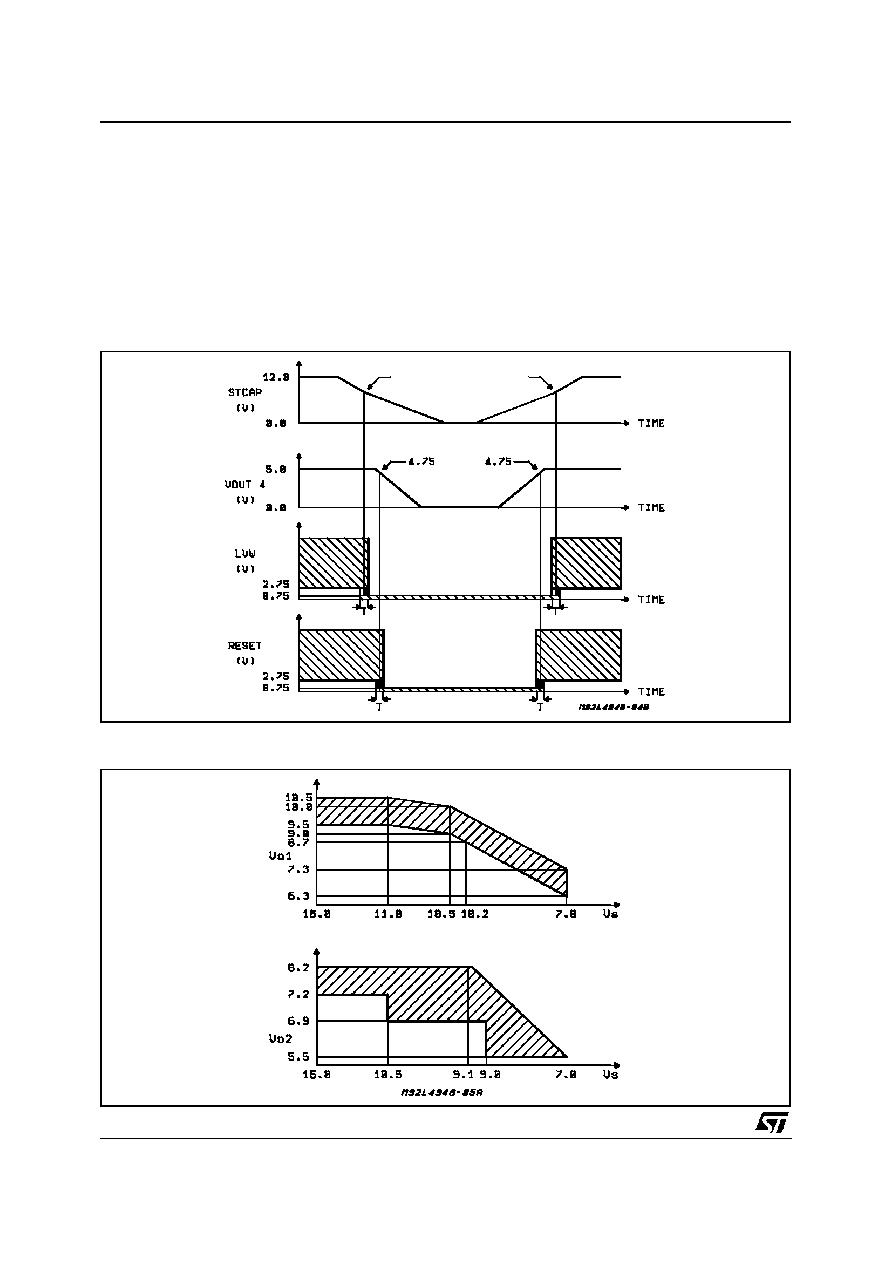
FUNCTIONAL DESCRIPTION
The L4946 includes a monitoring circuit to warn
the microprocessor if a low voltage or no voltage
condition is occurring. Between 7V and 8V on the
STCAP pin, the LVW output will go low. This tells
the microprocessor to stop executing code and
save vital information. The reset output will go low
when V
04
drops 0.15V below it's typical reading.
A reset will occur between a minimum of 4.5 and
a maximum of 5V on V
04
. The reset output will go
low when V
04
drops 0.15 below it's typical value.
A reset will occur between a minimum of 4.5V
and a maximum of 5V on V
04
. When the V
04
drops between 4.5 and 5V
the RESET output
goes low. It is very important that the RESET out-
put doesn't go above 0.75V until the V
04
output
has gone back above 4.75V (typical). The micro-
processor looks for a rising edge. So, any spike
will tell the microprocessor to start operating.
Once the STCAP line passes 7.5V (typical), the
LVW output will also return to high state.
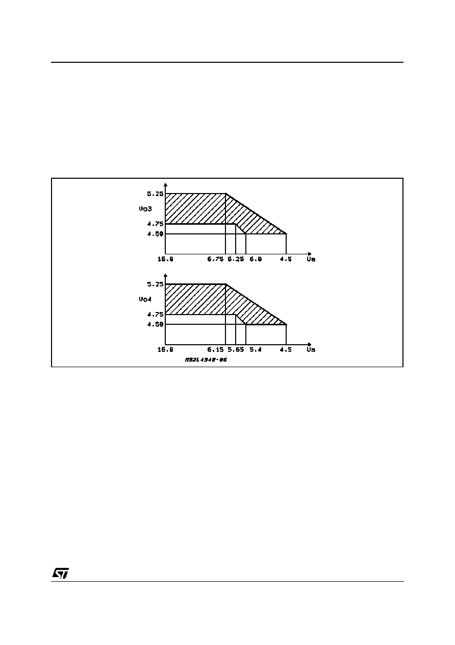
TIMING DIAGRAM
Graphs of the Output Curves for V
O1,2,3 and 4
5.0
5.0
7.5
7.5
150
µ
s
100
µ
s
150
µ
s
100
µ
s
L4946
6/9
The STCAP pin acts like a delay circuit. Due to
the large capacitor (470
µ
F), the STCAP pin allows
the battery voltage to decay slowly giving the mi-
croprocessor time to store data. Also, during short
low voltage or negative voltage conditions, the
STCAP pin protects the 5V st-by output from
dropping below the RESET and LVW trip points
The four outputs are expected to follow the bat-
tery voltage down to 7V. At 7V typical the LVW
tells the microprocessor to stop operation and
save operating data Below 7V the outputs are ex-
pected to stay alive and ready for a return of bat-
tery.
The L4946 has a st-by mode to keep the micro-
processor and memories allive during an ignition
off conditions. The ON/OFF input pin in controlled
by the microprocessor. An high on the ON/OFF
pin places the part in normal mode. A low on the
ON/OFF pin places the part in st-by mode.V
01
,
V
02
, V
03
will be off during st-by mode.
Graphs of the Output Curves for V
O1,2,3 and 4 (Cont.)
Notes and Information
The following information is for clarification, not for specification definition.
Please use the information in this way.
L4946
7/9

Multiwatt11 V
DIM.
mm
inch
MIN.
TYP.
MAX.
MIN.
TYP.
MAX.
A
5
0.197
B
2.65
0.104
C
1.6
0.063
D
1
0.039
E
0.49
0.55
0.019
0.022
F
0.88
0.95
0.035
0.037
G
1.45
1.7
1.95
0.057
0.067
0.077
G1
16.75
17
17.25
0.659
0.669
0.679
H1
19.6
0.772
H2
20.2
0.795
L
21.9
22.2
22.5
0.862
0.874
0.886
L1
21.7
22.1
22.5
0.854
0.87
0.886
L2
17.4
18.1
0.685
0.713
L3
17.25
17.5
17.75
0.679
0.689
0.699
L4
10.3
10.7
10.9
0.406
0.421
0.429
L7
2.65
2.9
0.104
0.114
M
4.25
4.55
4.85
0.167
0.179
0.191
M1
4.73
5.08
5.43
0.186
0.200
0.214
S
1.9
2.6
0.075
0.102
S1
1.9
2.6
0.075
0.102
Dia1
3.65
3.85
0.144
0.152
OUTLINE AND
MECHANICAL DATA
L4946
8/9

Information furnished is believed to be accurate and reliable. However, STMicroelectronics assumes no responsibility for the consequences
of use of such information nor for any infringement of patents or other rights of third parti es which may result from its use. No license is
granted by implication or otherwise under any patent or patent rights of STMicroelectronics. Specification mentioned in this publication are
subject to change without notice. This publication supersedes and replaces all information previously supplied. STMicroelectronics products
are not authorized for use as critical components in life support devices or systems without express written approval of STMicroelectronics.
The ST logo is a registered trademark of STMicroelectronics
©
2000 STMicroelectronics ≠ Printed in Italy ≠ All Rights Reserved
STMicroelectronics GROUP OF COMPANIES
Australia - Brazil - China - Finland - France - Germany - Hong Kong - India - Italy - Japan - Malaysia - Malta - Morocco -
Singapore - Spain - Sweden - Switzerland - United Kingdom - U.S.A.
http://www.st.com
L4946
9/9