 | –≠–ª–µ–∫—Ç—Ä–æ–Ω–Ω—ã–π –∫–æ–º–ø–æ–Ω–µ–Ω—Ç: L4949ED | –°–∫–∞—á–∞—Ç—å:  PDF PDF  ZIP ZIP |
L4949E
MULTIFUNCTION VERY LOW DROP
VOLTAGE REGULATOR
OPERATING DC SUPPLY VOLTAGE RANGE
5V - 28V
TRANSIENT SUPPLY VOLTAGE UP TO 40V
EXTREMELY LOW QUIESCENT CURRENT
IN STANDBY MODE
HIGH PRECISION STANDBY OUTPUT VOLT-
AGE 5V
±
1%
OUTPUT CURRENT CAPABILITY UP TO
100mA
VERY LOW DROPOUT VOLTAGE LESS
THAN 0.5V
RESET CIRCUIT SENSING THE OUTPUT
VOLTAGE
PROGRAMMABLE RESET PULSE DELAY
WITH EXTERNAL CAPACITOR
VOLTAGE SENSE COMPARATOR
THERMAL SHUTDOWN AND SHORT CIR-
CUIT PROTECTIONS
DESCRIPTION
The L4949E is a monolithic integrated 5V voltage
regulator with a very low dropout output and addi-
tional functions as power-on reset and input volt-
age sense. It is designed for supplying the micro-
computer
controlled
systems
especially
in
automotive applications.
June 2000
Æ
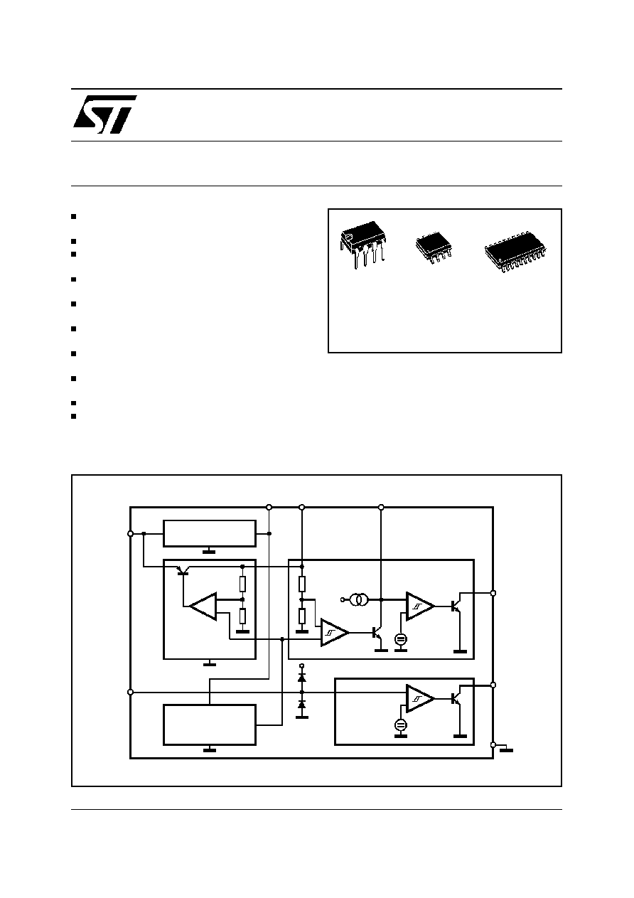
REG
1.23V
REF
SI
SO
RES
GND
D96AT219
PREREGULATOR 5V
V
S
2
µ
+
RESET
2V
SENSE
V
S
1.23V
CT
V
OUT
V
Z
BLOCK DIAGRAM
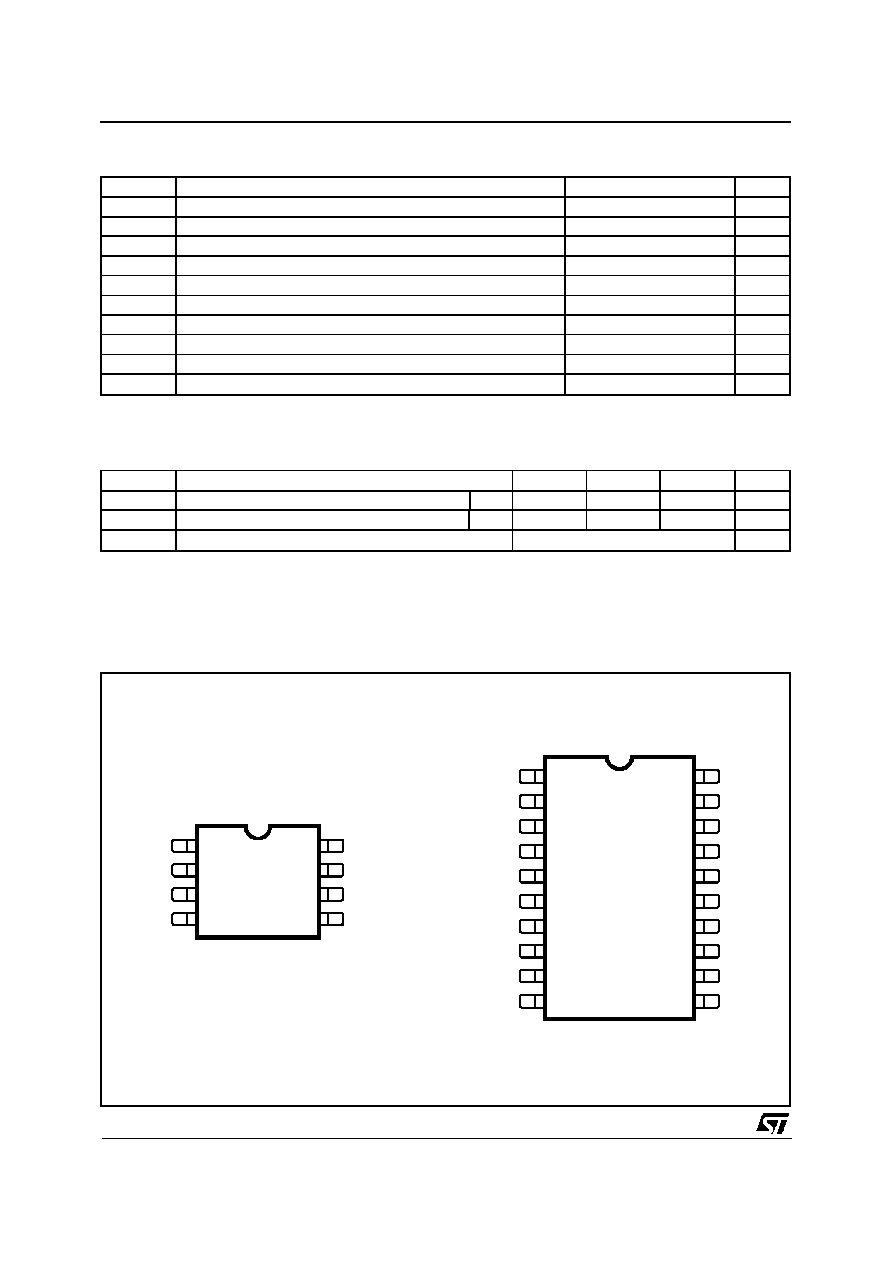
ORDERING NUMBERS: L4949E (Minidip)
L4949ED (SO8)
L4949EP (SO20W)
Minidip
SO8
SO20W (12+4+4)
1/10
ABSOLUTE MAXIMUM RATINGS
Symbol
Parameter
Value
Unit
V
SDC
DC Operating Supply Voltage
28
V
V
STR
Transient Supply Voltage (T < 1s)
40
V
I
O
Output Current
Internally Limited
V
O
Output Voltage
20
V
V
RES
, V
SO
Output Voltage
20
V
I
RES
, I
SO
Output Current
5
mA
V
Z
Preregulator Output Voltage
7
V
I
Z
Preregulator Output Current
5
mA
T
J
Junction Temperature
-40 to +150
∞
C
T
stg
Storage Temperature Range
-55 to +150
∞
C
Note: The circuit is ESD protected according to MIL-STD-883C
THERMAL DATA
Symbol
Description
Minidip
SO-8
SO20L
Unit
R
th j-amb
Thermal Resistance Junction-ambient
Max
100
200
50
∞
C/W
R
th j-pins
Thermal Resistance Junction-pins
Max
15
∞
C/W
TJSD
Thermal Shutdown Junction temperature
165
∞
C
PIN CONNECTIONS
VS
SI
V
Z
CT
GND
RES
SO
V
OUT
1
3
2
4
6
5
7
8
D95AT217
V
Z
CT
N.C.
GND
GND
GND
GND
N.C.
N.C.
V
OUT
N.C.
GND
GND
GND
GND
N.C.
V
S
SI
1
3
2
4
5
6
7
8
9
18
17
16
15
14
12
13
11
19
10
20
RES
SO
D95AT218
MINIDIP/SO8
SO20
L4949E
2/10
ELECTRICAL CHARACTERISTICS (V
S
= 14V; -40
∞
C < T
j
< 125
∞
C unless otherwise specified)
Symbol
Parameter
Test Condition
Min.
Typ.
Max.
Unit
V
O
Output Voltage
T
J
= 25
∞
C; I
O
= 1mA
4.95
5
5.05
V
V
O
Output Voltage
6V < V
IN
< 28V, 1mA < I
O
< 50mA
4.90
5
5.10
V
V
O
Output Voltage
V
IN
= 40V;
T < 1s 5mA < I
O
<100mA
4.75
5.25
V
V
DP
Dropout Voltage
I
O
= 10mA
I
O
= 50mA
I
O
= 100mA
0.1
0.2
0.3
0.25
0.4
0.5
V
V
V
V
IO
Input to Output Voltage
Difference in Undervoltage
Condition
V
IN
= 4V, I
O
= 35mA
0.4
V
I
outh
**
Max Output Leakage
V
IN
= 25V, V
O
= 5.5V
20
50
80
µ
A
V
OL
Line Regulation
6V < V
IN
< 28V; I
O
= 1mA
20
mV
V
OLO
Load Regulation
1mA < I
O
< 100mA
30
mV
I
LIM
Current Limit
V
O
= 4.5V
V
O
= 4.5V, T
J
= 25
∞
C
V
O
= 0V (note 1)
105
120
200
100
400
400
mA
mA
mA
I
QSE
Quiescent Current
I
O
= 0.3mA; T
J
< 100
∞
C
200
300
µ
A
I
Q
Quiescent Current
I
O
= 100mA
5
mA
** With this test we guarantee that with no output current the output voltage will not exceed 5.5V
RESET
V
RT
Reset Thereshold Voltage
V
O
-0.5V
V
V
RTH
Reset Thereshold Hysteresis
50
100
200
mV
t
RD
Reset Pulse Delay
C
T
= 100nF; T
R
100
µ
s
55
100
180
ms
V
RL
Reset Output Low Voltage
R
RES
= 10K
to V
O
V
S
1.5V
0.4
V
I
RH
Reset Output High Leakage Current V
RES
= 5V
1
µ
A
V
CTth
Delay Comparator Thereshold
2
V
V
CTth, hy
Delay Comparator Thereshold
Hysteresis
100
mV
SENSE
V
st
Sense Low Thereshold
1.16
1.23
1.35
V
V
sth
Sense Thereshold Hysteresis
20
100
200
mV
V
SL
Sense Output Low Voltage
V
SI
1.16V; V
S
3V
R
SO
= 10K
to V
O
0.4
V
I
SH
Sense Output Leakage
V
SO
= 5V; V
SI
1.5V
1
µ
A
I
SI
Sense Input Current
V
SI
= 0
-20
-8
-3
µ
A
PREREGULATOR
V
Z
Preregulator Output Voltage
I
Z
= 10
µ
A
4.5
5
6
V
I
Z
Preregulator Output Current
10
µ
A
Note 1: Foldback characteristic
L4949E
3/10
APPLICATION INFORMATION
Supply Voltage Transient
High supply voltage transients can cause a reset
output signal disturbation.
For supply voltages greater than 8V the circuit
shows a high immunity of the reset output against
supply transients of more than 100V/
µ
s.
For supply voltages less than 8V supply tran-
sients of more than 0.4V/
µ
s can cause a reset
signal disturbation.
To improve the transient behaviour for supply
voltages less than 8V a capacitor at pin 3 can be
used.
A capacitor at pin 3 (C3
1
µ
F) reduces also the
output noise.
FUNCTIONAL DESCRIPTION
The L4949E is a monolithic integrated voltage
regulator, based on the STM modular voltage
regulator approch. Several outstanding features
and auxiliary functions are implemented to meet
the requirements of supplying microprocessor
systems in automotive applications. Nevertheless,
it is suitable also in other applications where the
present functions are required. The modular ap-
proach of this device allows to get easily also
other features and functions when required.
Voltage Regulator
The voltage regulator uses an Isolated Collector
Vertical PNP transistor as a regulating element.
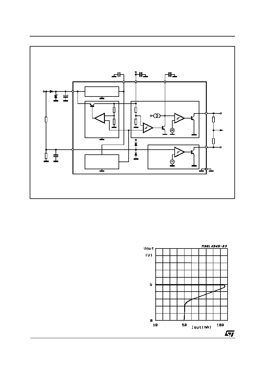
Figure 1: Foldback Characteristic of V
O
REG
1.23V
REF
SI
SO
RES
GND
D96AT219
PREREGULATOR 5V
V
S
2
µ
+
RESET
2V
SENSE
V
S
1.23V
V
OUT
V
Z (optional)
V
BAT
CT
V
OUT
APPLICATION CIRCUIT
For stability: C
S
1
µ
F, C
O
4.7
µ
F, ESR < 10
at 10KHz
Recommended for application: C
S
= C
O
= 10
µ
F to 100
µ
F
L4949E
4/10
With this structure very low dropout voltage at
currents up to 100mA is obtained. The dropout
operation of the standby regulator is maintained
down to 3V input supply voltage. The output volt-
age is regulated up to the transient input supply
voltage of 40V. With this feature no functional in-
terruption due to overvoltage pulses is generated.
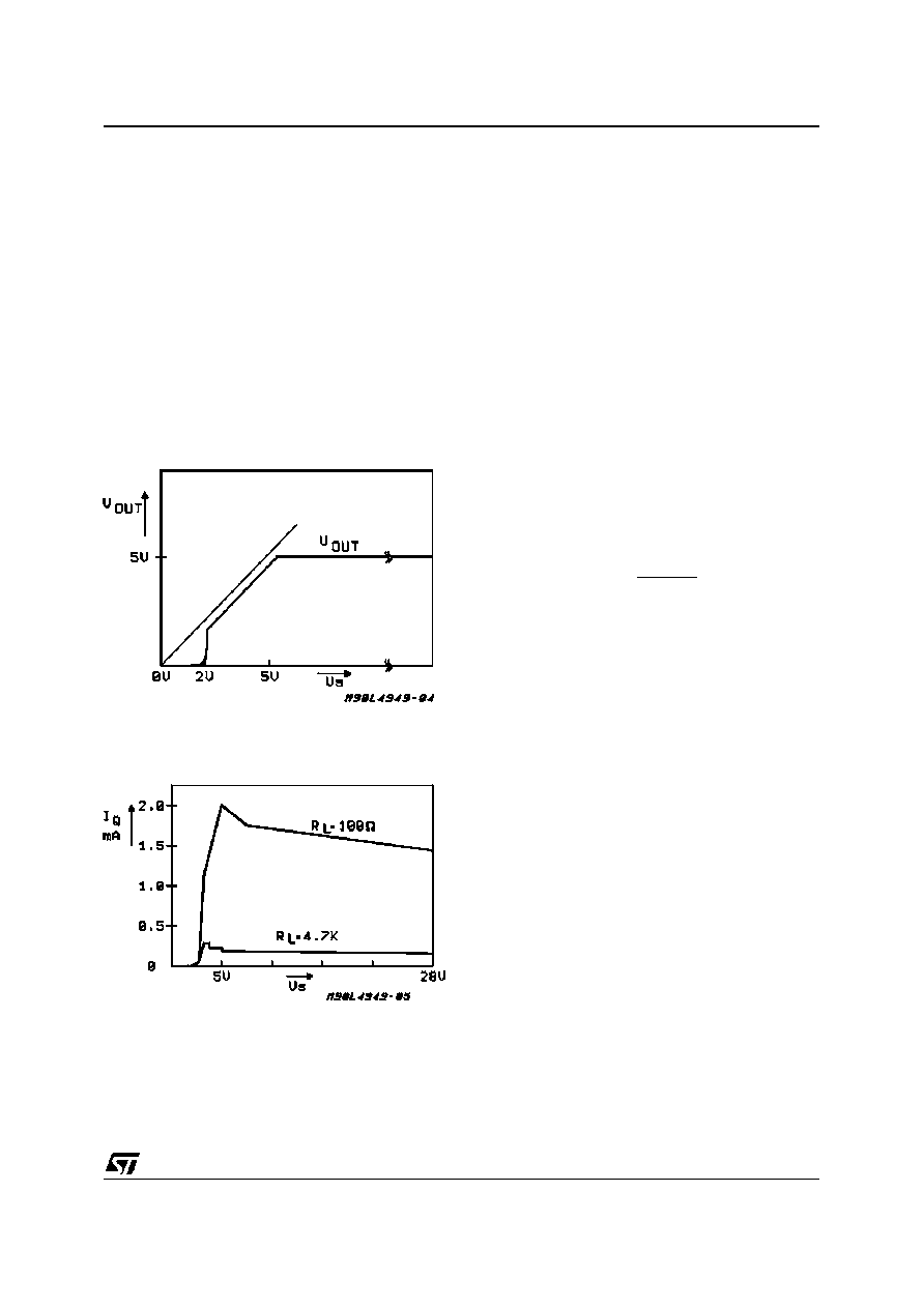
The typical curve showing the standby output
voltage as a function of the input supply voltage is
shown in Fig. 2. The current consumption of the
device (quiescent current) is less than 300
µ
A.
To reduce the quiescent current peak in the un-
dervoltage region and to improve the transient re-
sponse in this region, the dropout voltage is con-
trolled, the quiescent current as a function of the
supply input voltage is shown in Fig. 3.
Preregulator
To improve the transient immunity a preregulator
stabilized the internal supply voltage to 5V. This
internal voltage is present at Pin 3 (V
Z
). This volt-
age should not be used as an output because the
output capability is very small (
10
µ
A).
This output may be used as an option when a
better transient behaviour for supply voltages less
than 8V is required (see also application note).
In this case a capacitor (100nF - 1
µ
F) must be
connected between Pin 3 and GND. If this feature
is not used Pin 3 must be left open.
Reset Circuit
The block circuit diagram of the reset circuit is
shown in Fig. 4. The reset circuit supervises the
output voltage.
The reset thereshold of 4.5V is defined with the
internal reference voltage and standby output
drivider.
The reset pulse delay time t
RD
, is defined with the
charge time of an external capacitor C
T
:
t
RD
=
C
T
∑
2V
2
µ
A
The reaction time of the reset circuit originates
from the discharge time limitation of the reset ca-
pacitor C
T
and is proportional to the value of C
T
.
The reaction time of the reset circuit increases the
noise immunity. Standby output voltage drops be-
low the reset threshold only a bit longer than the
reaction time results in a shorter reset delay time.
The nominal reset delay time will be generated for
standby output voltage drops longer than approxi-
mately 50
µ
s.
The typical reset output waveforms are shown in
Fig. 5.
Sense Comparator
The sense comparator compares an input signal
with an internal voltage reference of typical 1.23V.
The use of an external voltage divider makes this
comparator very flexible in the application.
It can be used to supervise the input voltage
either before or after the protection diode and to
give additional informations to the microprocessor
like low voltage warnings.
Figure 3: Quiescent Current vs. Supply Voltage
Figure 2: Output Voltage vs. Input Voltage
40V
L4949E
5/10