 | –≠–ª–µ–∫—Ç—Ä–æ–Ω–Ω—ã–π –∫–æ–º–ø–æ–Ω–µ–Ω—Ç: L4951 | –°–∫–∞—á–∞—Ç—å:  PDF PDF  ZIP ZIP |
L4945/L4950
L4951
5V/8.5V/10V VERY LOW DROP VOLTAGE REGULATORS
PRECISE OUTPUT VOLTAGE:
5V
±
4% (L4945)
8.5V
±
4% (L4950)
10V
±
4% (L4951)
OVER FULL TEMPERATURE RANGE
(≠ 40 / 125
∞
C)
VERY LOW VOLTAGE DROP (0.75Vmax)
OVER FULL TEMPERATURE RANGE
OUTPUT CURRENT UP TO 500mA
OVERVOLTAGE AND REVERSE VOLTAGE
PROTECTIONS
REVERSE VOLTAGE PROTECTION
SHORT CIRCUIT PROTECTION AND THER-
MAL SHUT-DOWN (with hysteresis)
LOW START UP CURRENT
DESCRIPTION
The devices are a monolithic integrated circuit in
Versawatt package specially designed to provide
a stabilized supply voltage for automotive and in-
dustrial electronic systems. Thanks to their very
low voltage drop, in automotive applications the
devices can work correctly even during the crank-
ing phase, when the battery voltage could fall as
low as 6V. Furthermore, they incorporate a com-
plete range of protection circuits against the dan-
gerous overvoltages always present on the bat-
tery rail of the car.
This is advanced information on a new product now in development or undergoing evaluation. Details are subject to change without notice.
October 1992
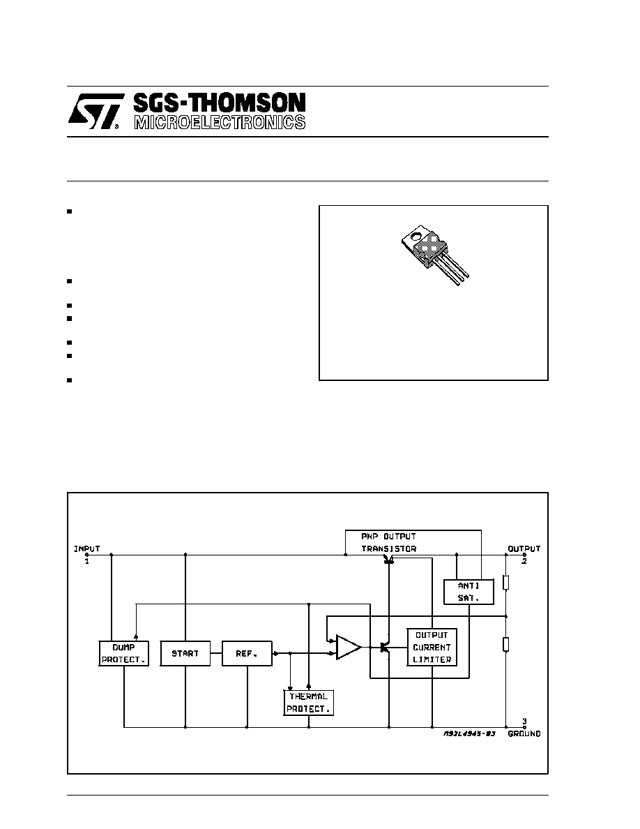
BLOCK DIAGRAM
TO220
ORDERING NUMBER: L4945
L4950
L4951
1/6
ABSOLUTE MAXIMUM RATINGS
Symbol
Parameter
Value
Unit
V
i
DC Input Voltage
DC Reverse Input Voltage
Transient Input Overvoltages :
Load Dump :
5ms
t
rise
10ms
f
Fall Time Constant = 100ms
R
SOURCE
0.5
Field Decay :
5ms
t
fa ll
10ms, R
SOURCE
10
r
Rise Time Constant = 33ms
Low Energy Spike :
t
rise
= 1
µ
s, t
fall
= 500
µ
s, R
SOURCE
10
f
r
Repetition Frequency = 5Hz
35
≠ 18
80
≠ 80
±
100
V
V
V
V
V
T
J
Junction Temperature Range
≠ 40 to 150
∞
C
T
OP
Operating Temperature Range
≠ 40 to 125
∞
C
T
stg
Storage Temperature Range
≠ 55 to 150
∞
C
Note: The circuit is ESD protected according to MIL-STD-883C.
THERMAL DATA
Symbol
Parameter
Value
Unit
R
th j-case
Thermal Resistance Junction-case
Max
3
∞
C/W
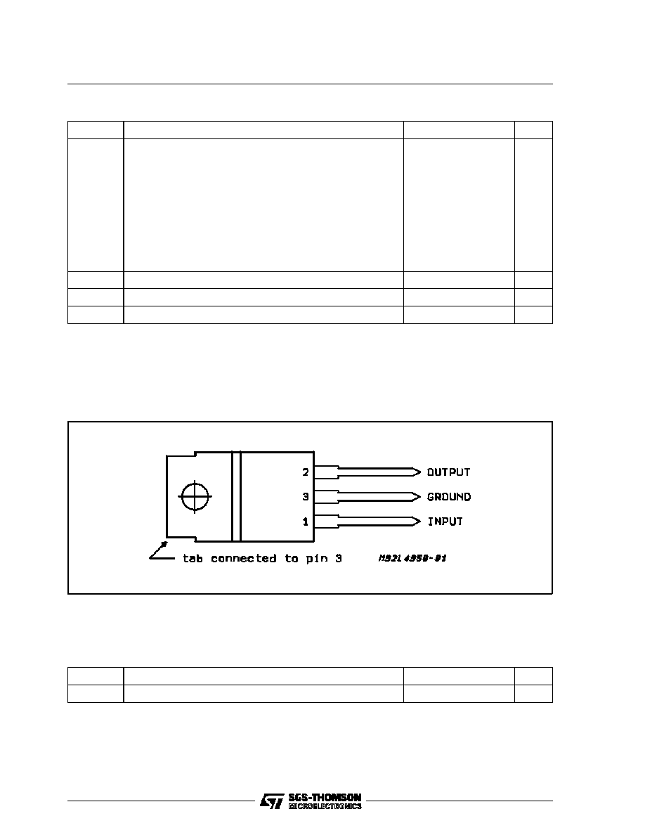
PIN CONNECTION (Top view)
L4945 - L4950 - L4951
2/6
FUNCTIONAL DESCRIPTION
The block diagram shows the basic structure of
the devices : the reference, the error amplifier, the
driver, the power PNP, the protection and reset
functions.
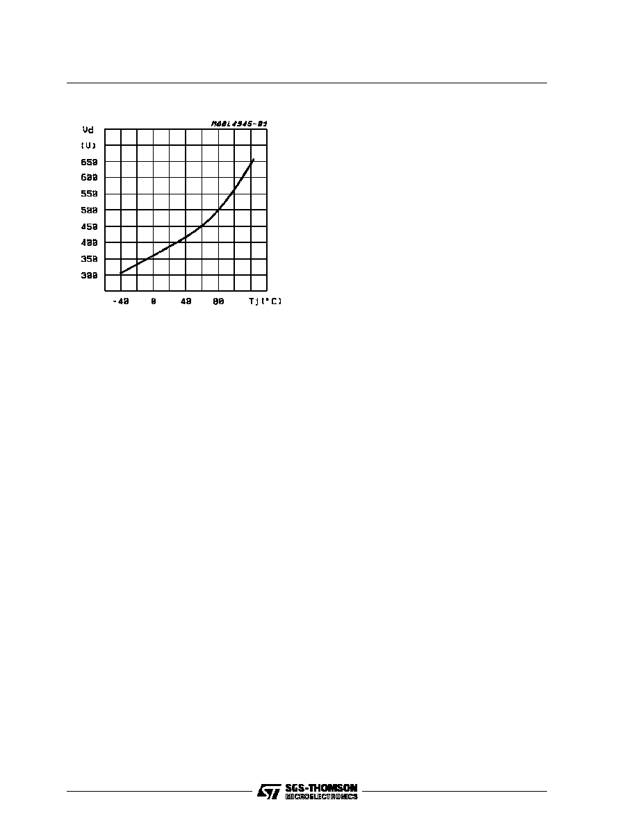
The power stage is a Lateral PNP transistor
which allows a very low dropout voltage (typ.
400mV at T
J
= 25
∞
C, max. 750mV over the full
temperature range @ I
O
= 500mA). The typical
curve of the dropout voltage as a function of the
junction temperature is shown in Fig. 1 : that is
the worst case, where I
O
= 500mA.
The current consumption of the devices (quies-
cent current) are maximum 10mA - over full T -
when no load current is required.
The internal antisaturation circuit allows a drastic
reduction in the current peak which takes place
during the start up.
The three gain stages (operational amplifier,
driver and power PNP) require the external ca-
pacitor (C
omin
= 20
µ
F) to guarantee the global
stability of the system.
Load dump and field decay protections (
±
80V, t =
300ms), reverse voltage (≠ 18V) and short circuit
protection, thermal shutdown are the main fea-
tures that make the devices specially suitable for
applications in the automotive enviroment.
ELECTRICAL CHARACTERISTICS (refer to the test circuit, V
i
= 14. 4V, C
o
= 47
µ
F, ESR < 10
,
R
p
= 1K
, R
L
= 1K
, ≠40
∞
C
T
J
125
∞
C, unless otherwise specified)
Symbol
Parameter
Test Conditions
Min.
Typ.
Max.
Unit
V
o
Output Voltage
I
o
= 0mA to 500mA
Over Full T Range for L4945
for L4950
for L4951
4.80
8.16
9.60
5.00
8.50
10
5.20
8.84
10.4
V
V
V
T
j
= 25
∞
C
for L4945
for L4950
for L4951
4.90
8.33
9.80
5.00
8.50
10
5.10
8.67
10.2
V
V
V
V
i
Operating Input Voltage
I
o
= 0mA to (*) 500mA
6
26
V
V
o
Line Regulation
V
i
= 6V to 26V ;
I
o
= 5mA
2
10
mV
V
o
Load Regulation
I
o
= 5mA to 500mA
15
60
mV
V
i
≠V
o
Dropout Voltage
I
o
= 500mA, T
J
= 25
∞
C
Over Full T Range
0.40
0.55
0.75
V
V
I
q
Quiescent Current
I
o
= 0mA, T
J
= 25
∞
C
I
o
= 0mA Over Full T
I
o
= 500mA Over Full T
5
6.5
110
10
13
180
mA
mA
mA
Temperature Output Voltage
Drift
≠ 0.5
mV/
∞
C
SVR
Supply Volt. Rej.
I
o
= 350mA ; f = 120Hz
C
o
= 100
µ
F ;
V
i
= 12V
±
5V
pp
50
60
dB
I
sc
Output Short Circuit Current
0.50
0.80
1.50
A
(*) For a DC voltage 26 < V
i
< 37V the device is not operating
V
o
T
TEST CIRCUIT
L4945 - L4950 - L4951
3/6
EXTERNAL COMPENSATION
Since the purpose of a voltage regulator is to sup-
ply and load variations, the open loop gain of the
regulators must be very high at low frequencies.
This may cause instability as a result of the vari-
ous poles present in the loop. To avoid this insta-
bility dominant pole compensation is used to re-
duce phase shift due to other poles at the unity
gain frequency. The lower the frequency of these
others poles at the unity gain frequency. The
lower the frequency of these other poles, the
greater must be capacitor esed to create the
dominant pole for the same DC gain.
Where the output transistor is a lateral PNP type
there is a pole in the regulation loop at a fre-
quencybtoo low to be compensated by a capaci-
tor which can be integrated. An external compen-
sation is therefore necessary so a very high value
capacitor must be connected from the output to
ground.
The paeassitic equivalent series resistance of the
capacitor used adds a zero to the regulation loop.
This zero may compromise the stability of the
system since its effect tends to cancel the effect
of the pole added. In regulators this ESR must be
less than 3
and the minimum capacitor value is
47
µ
F.
Figure 1: Typical Dropout Voltage vs. T
j
(I
o
= 500mA).
L4945 - L4950 - L4951
4/6
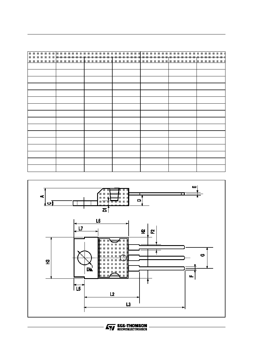
TO220 (VERSAWATT) PACKAGE MECHANICAL DATA
DIM.
mm
inch
MIN.
TYP.
MAX.
MIN.
TYP.
MAX.
A
4.8
0.189
C
1.37
0.054
D
2.4
2.8
0.094
0.110
D1
1.2
1.35
0.047
0.053
E
0.35
0.55
0.014
0.022
F
0.8
1.05
0.031
0.041
F2
1.15
1.4
0.045
0.055
G
4.95
5.08
5.21
0.195
0.200
0.205
H2
10.4
0.409
H3
10.05
10.4
0.396
0.409
L2
16.2
0.638
L3
26.3
26.7
27.1
1.035
1.051
1.067
L5
2.6
3
0.102
0.118
L6
15.1
15.8
0.594
0.622
L7
6
6.6
0.236
0.260
Dia
3.65
3.85
0.144
0.152
L4945 - L4950 - L4951
5/6

Information furnished is believed to be accurate and reliable. However, SGS-THOMSON Microelectronics assumes no responsibility for the
consequences of use of such information nor for any infringement of patents or other rights of third parties which may result from its use. No
license is granted by implication or otherwise under any patent or patent rights of SGS-THOMSON Microelectronics. Specifications men-
tioned in this publication are subject to change without notice. This publication supersedes and replaces all information previously supplied.
SGS-THOMSON Microelectronics products are not authorized for use as critical components in life support devices or systems without ex-
press written approval of SGS-THOMSON Microelectronics.
©
1994 SGS-THOMSON Microelectronics - All Rights Reserved
SGS-THOMSON Microelectronics GROUP OF COMPANIES
Australia - Brazil - France - Germany - Hong Kong - Italy - Japan - Korea - Malaysia - Malta - Morocco - The Netherlands - Singapore -
Spain - Sweden - Switzerland - Taiwan - Thaliand - United Kingdom - U.S.A.
L4945 - L4950 - L4951
6/6