 | –≠–ª–µ–∫—Ç—Ä–æ–Ω–Ω—ã–π –∫–æ–º–ø–æ–Ω–µ–Ω—Ç: L4953 | –°–∫–∞—á–∞—Ç—å:  PDF PDF  ZIP ZIP |
L4953
MULTIFUNCTION VOLTAGE REGULATOR FOR CAR RADIO
3 OUTPUTS:
10V (500mA); 5V (1A); 5V (100mA) STANDBY
OUT1 (10V) AND OUT2 (5V) WITH INDE-
PENDENT ENABLE CONTROL FOR STAND-
BY MODE
3A HIGH SIDE DRIVER WITH CLAMPED
OUTPUT (16V)
LOGIC OUTPUT FOR:
≠ SUPPLY UNDERVOLTAGE (LVW)
≠ OVERVOLTAGE
≠ THERMAL PROTECTION
RESET FUNCTION
IGNITION COMPARATOR
REVERSE BATTERY AND LOAD DUMP
PROTECTION
THERMAL SHUTDOWN
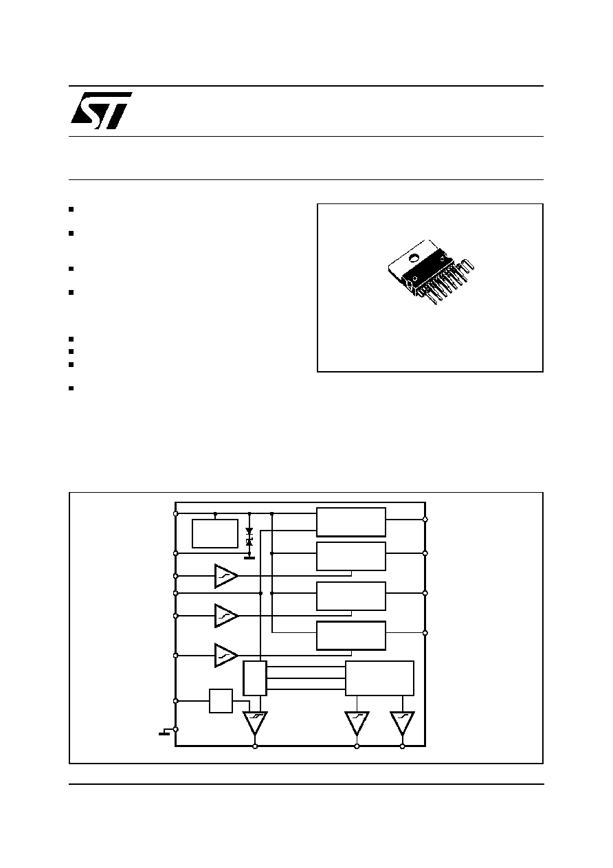
DESCRIPTION
The L4953 contains a triple voltage regulator and
a power switch.
The IC includes a monitoring circuit to warn if a
low voltage or no voltage condition is occuring.
In stand-by output is active as long as possible
even when in thermal shutdown or any other fault
conditions.
The STCAP pin allows the use of a reserve sup-
ply capacitor that will hold enough energy for the
5V Stand-by line to allow the
µ
P to store data.
June 2000
Æ
5V, 100mA
REGULATOR
STAND-BY
LOAD DUMP
AND REV
BATT PROT
REF
GEN
5V, 1000mA
REGULATOR
SWITCHED
10V, 500mA
REGULATOR
SWITCHED
16V, 3A
VOLTAGE CLAMP
SWITCHED
OVERVOLTAGE
UNDERVOLTAGE
THERMAL PROT
RESET
VCAP
Vref1 LVW THRESHOLD
Vref2 Reset THRESHOLD
IGNITION THRESHOLD
PROT
VS
7
POW GND
3
EN 5V
1
STCAP
12
EN 10V
2
EN 16V
15
11
STAND-BY 5V
9
OUT 5V
10
OUT 10V
4
OUT 16V
14
13
6
IGN OUT
LVW/FAULT
RESET
IGN INP
5
D94AU053A
SIG GND
8
BLOCK DIAGRAM
Multiwatt 15
ORDERING NUMBER: L4953
1/6
ABSOLUTE MAXIMUM RATINGS
Symbol
Parameter
Value
Unit
V
SDC
DC Operating Supply Voltage
≠14 to 28
V
V
STR
Transient Supply Voltage
50
V
I
O
Output Current
internally limited
T
op
Operating Temperature Range
≠40 to 85
∞
C
T
stg
Storage Temperature
≠55 to 150
∞
C
THERMAL DATA
Symbol
Parameter
Value
Unit
R
th j-case
Thermal Resistance Junction-case
2
∞
C/W
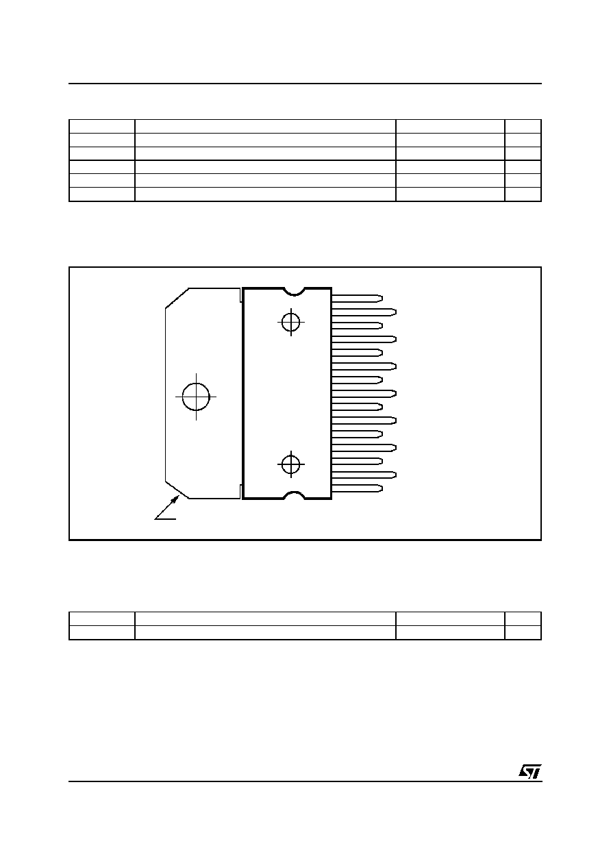
1
2
3
4
5
6
7
9
10
11
8
STBY5V
OUT 8.25V
OUT 5V
PGND
VS
IGNOUT
IGNINP
OUT 16V
SGND
EN 8.25V
EN 5V
TAB CONNECTED TO PIN 8
13
14
15
12
EN 16V
RESET
LVW/FAULT
STCAP
D94AU054B
PIN CONNECTION (Top view)
L4953
2/6
ELECTRICAL CHARACTERISTICS (V
S
= 14V, T
amb
= 25
∞
C, unless otherwise specified.)
Symbol
Parameter
Test Condition
Min.
Typ.
Max.
Unit
V
S
Operating Supply Voltage
11
18
V
En
Output Noise Voltage
Any reg. supply,
f = 100Hz to 200KHz
200
400
µ
V
5V STAND-BY OUTPUT VOLTAGE
V
5st-by
Stand-by Output Voltage
No load
4.75
5
5.25
V
V
line
Line Regulation
11V < V
S
< 16V
5
50
mV
V
load
Load Regulation
5mA < I
O
< 100mA
45
150
mV
V
dropout
Dropout Voltage
I
out
= 100mA V
S
= 5.5V
0.2
0.6
V
I
qst-by
Quiescent Current @ Stand-by
I
L
= 5mA
0.3
0.65
mA
5V/1000mA SWITCHED OUTPUT VOLTAGE
V
out5
5V Output Voltage
no load
4.75
5
5.25
V
V
line
Line Regulation
7V < V
S
< 18V
5
50
mV
V
load
Load Regulation
5mA < I
O
< 1A
12
50
mV
V
dropout
Dropout Voltage
I
O
= 1A V
S
= 5,5V
1
1.5
V
I
q
Quiescent Current
I
O
= 1A
30
100
mA
I
lim
Current Limit
Output Shorted to GND
1
1.3
A
SWon
Switch ON
3.5
V
SW off
Switch OFF
1.5
V
SW hyst
Switch Hysteresis
100
200
500
mV
R
in
Input Impedance
10
40
K
10V/500mA SWITCHED OUTPUT VOLTAGE
V
out10
10V Output Voltage
no load
9.5
10
10.5
V
V
line
Line Regulation
11V < V
S
< 18V
5
50
mV
V
load
Load Regulation
5mA < I
O
< 500mA
12
50
mV
V
dropout
Dropout Voltage
5.5V < V
S
< 10V I
O
= 500mA
0.4
0.9
V
I
q
Quiescent Current
I
O
= 500mA
10
50
mA
I
lim
Current Limit
Output Shorted to GND
500
600
mA
SVR
Supply Voltage Rejection
f = 3KHz
45
dB
SWon
Switch ON
3.5
V
SW off
Switch OFF
1.5
V
SW hyst
Switch Hysteresis
100
200
500
mV
R
in
Input Impedance
10
40
K
HIGH SIDE DRIVER WITH CLAMPED OUTPUT (16V)
V
out16
Max. Output Voltage
V
S
= 18V
14.6
16.2
V
I
O
Output Continuous Current
V
S
= 16V
2
A
V
dropout
Dropout Voltage
6V < V
in
< 15V
I
O
= 1A
0.4
0.9
V
SWon
Switch ON
3.5
V
SW off
Switch OFF
1.5
V
SW hyst
Switch Hysteresis
100
200
500
mV
R
in
Input Impedance
10
40
K
L4953
3/6
ELECTRICAL CHARACTERISTICS (continued)
FAULT
Symbol
Parameter
Test Condition
Min.
Typ.
Max.
Unit
TH
fault
Fault Threshold
7
8.5
V
HYST
fault
Fault Threshold Hysteresis
100
200
300
mV
OUT
fault
Fault Output Voltage
1.5
V
I
leak
Fault Leakage Current
50
µ
A
RESET
THON
reset
Reset ON Threshold
4.5
5.15
V
HYST
reset
Reset Threshold Hysteresis
75
175
300
mV
OUT
reset
Reset Output Voltage
1.5
V
I
leak
Reset Leakage Current
5
µ
A
IGNITION
TH
ign
Ign Comparator Positive
Threshold
5.5
6
7.5
V
HYST
ign
Ign Comparator Threshold
Hysteresis
100
300
500
mV
IGN
high
Ignition Comparator Output High
3.5
Vst-by
V
IGN
low
Ignition Comparator Output Low
≠0.5
1.5
V
L4953
4/6
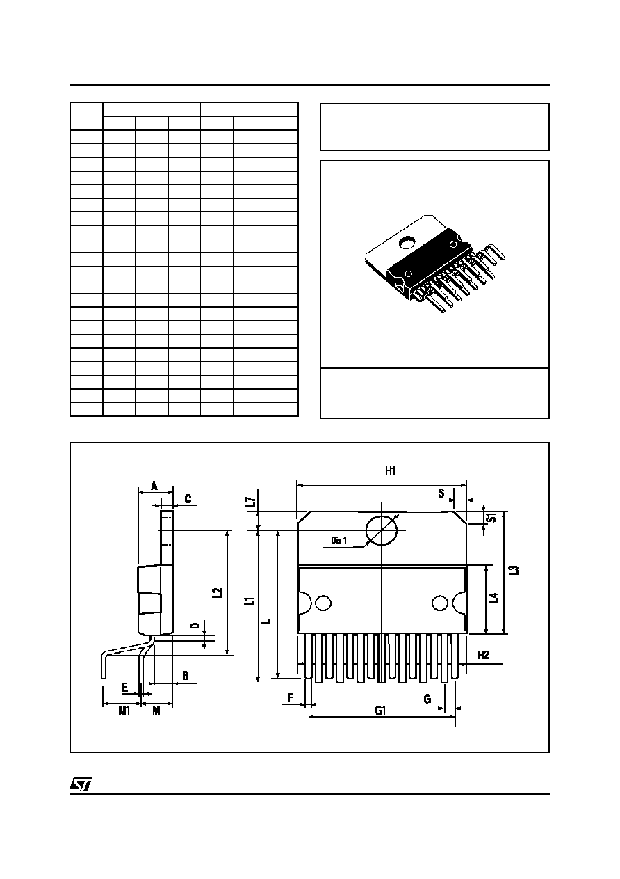
Multiwatt15 V
DIM.
mm
inch
MIN.
TYP.
MAX.
MIN.
TYP.
MAX.
A
5
0.197
B
2.65
0.104
C
1.6
0.063
D
1
0.039
E
0.49
0.55
0.019
0.022
F
0.66
0.75
0.026
0.030
G
1.02
1.27
1.52
0.040
0.050
0.060
G1
17.53
17.78
18.03
0.690
0.700
0.710
H1
19.6
0.772
H2
20.2
0.795
L
21.9
22.2
22.5
0.862
0.874
0.886
L1
21.7
22.1
22.5
0.854
0.870
0.886
L2
17.65
18.1
0.695
0.713
L3
17.25
17.5
17.75
0.679
0.689
0.699
L4
10.3
10.7
10.9
0.406
0.421
0.429
L7
2.65
2.9
0.104
0.114
M
4.25
4.55
4.85
0.167
0.179
0.191
M1
4.63
5.08
5.53
0.182
0.200
0.218
S
1.9
2.6
0.075
0.102
S1
1.9
2.6
0.075
0.102
Dia1
3.65
3.85
0.144
0.152
OUTLINE AND
MECHANICAL DATA
L4953
5/6

Information furnished is believed to be accurate and reliable. However, STMicroelectronics assumes no responsibility for the consequences
of use of such information nor for any infringement of patents or other rights of third parti es which may result from its use. No license is
granted by implication or otherwise under any patent or patent rights of STMicroelectronics. Specification mentioned in this publication are
subject to change without notice. This publication supersedes and replaces all information previously supplied. STMicroelectronics products
are not authorized for use as critical components in life support devices or systems without express written approval of STMicroelectronics.
The ST logo is a registered trademark of STMicroelectronics
©
2000 STMicroelectronics ≠ Printed in Italy ≠ All Rights Reserved
STMicroelectronics GROUP OF COMPANIES
Australia - Brazil - China - Finland - France - Germany - Hong Kong - India - Italy - Japan - Malaysia - Malta - Morocco -
Singapore - Spain - Sweden - Switzerland - United Kingdom - U.S.A.
http://www.st.com
L4953
6/6