 | –≠–ª–µ–∫—Ç—Ä–æ–Ω–Ω—ã–π –∫–æ–º–ø–æ–Ω–µ–Ω—Ç: L4955 | –°–∫–∞—á–∞—Ç—å:  PDF PDF  ZIP ZIP |
L4955
5A ULDO LINEAR REGULATORS FAMILY
UP TO 5A OUTPUT CURRENT
±
2% PRECISE OUTPUT VOLTAGES
FAST TRANSIENT RESPONSE
0.75V TYP. DROP OUT VOLTAGE AT 5A
OPERATING INPUT VOLTAGE FROM 4.5V
ADJUSTABLE VERSION:
∑
V
O
= 1.26V
∑
INHIBIT (I
Q
= 120
µ
A TYP.)
∑
POWER GOOD
∑
PROGRAMMABLE CURRENT LIMIT
∑
HEPTAWATT PACKAGE
FIXED VERSION:
∑
3.3V, 5.1V OUTPUTS
∑
VERSAWATT PACKAGE
VERY LOW QUIESCENT CURRENT
SHORT CIRCUIT PROTECTION (Foldback
function)
THERMAL SHUTDOWN
APPLICATIONS
PENTIUM
TM
AND POWER PC
TM
SUPPLIES
POST REGULATOR FOR SMPS
LOW COST SOLUTION FOR 5V TO 3.3V
CONVERSION
LOW COST BATTERY CHARGER
CONSTANT CURRENT REGULATOR
SUITABLE FOR APPLICATION WITH
STANDBY FEATURE
DESCRIPTION
The L4955 is a family of monolithic ultra very low
drop linear regulators designed to supply the
most recent microprocessors.
The dropout voltage is only 0.75V (Typ.) at 5A, di-
rectly dependent on the output current conditions.
Realized in BCDII technology, it has on board a
charge pump to properly drive an N-channel
power mos Transistor with 150m
of R
DSON
.
It operates from a 4.5V minimum supply, with a
very low quiescent current irrespective of the
load; a minimum of 22
µ
F output capacitor is re-
quired for stability.
The on-chip trimming techniques improve the pre-
cision of the available output voltages to
±
2%.
Ancillary functions like power good, inhibit with
low power consumption, programmable output
voltage and current limiting make the flexible
heptawatt version usable in applications where
power management, stand-by, features, post
regulation and adjustable current generators for
battery chargers are important.
February 1999
Æ
TYPICAL APPLICATIONS
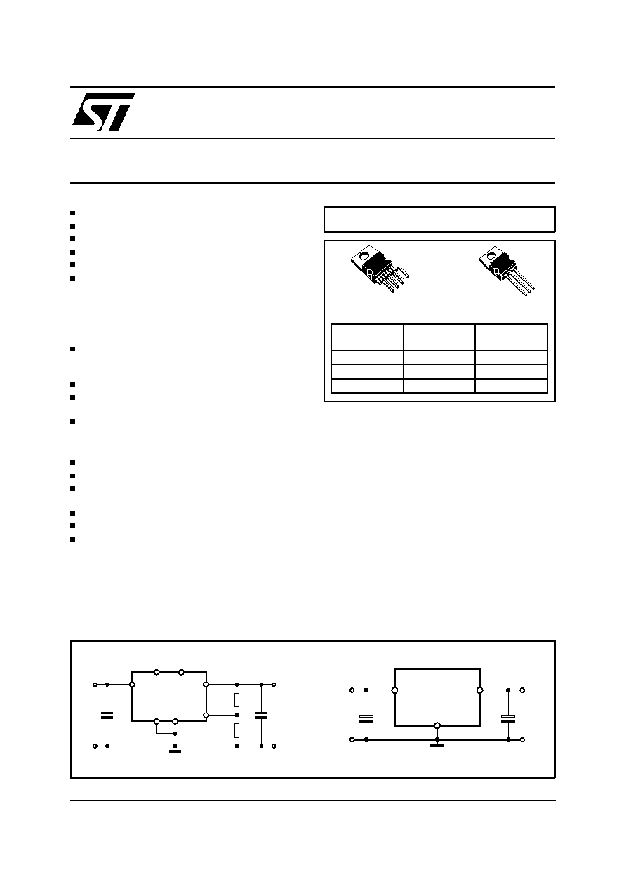
HEPTAWATT VERSAWATT
(TO-220)
MULTIPOWER BCD TECHNOLOGY
ORDERING
NUMBERS
OUTPUT
VOLTAGE
PACKAGE
L4955
1.26V ADJ
HEPTAWATT
L4955V3.3
3.3V
VERSAWATT
L4955V5.1
5.1V
VERSAWATT
L4955
CL
GND
ADJ
OUT
IN
INH
PG
7
5
2
4
6
3
1
C1
V
IN
R1
R2
C2
V
OUT
D97IN589
L4955VXXX
GND
OUT
IN
3
2
1
C1
V
IN
C2
V
OUT
D97IN590
1/14
VERSAWATT
(TO220)
ABSOLUTE MAXIMUM RATINGS
Symbol
Parameter
Value
Unit
V
IN
Supply Input Voltage
24
V
ADJ and CL pins
PG and INH pins
-0.3 to 4
0 to V
IN
V
V
P
TOT
Power Dissipation @ T
amb
= 50∞C
Power Dissipation @ T
case
= 90∞C
2
15
W
W
T
st
, T
i
Storage Temperature
-40 to +150
∞C
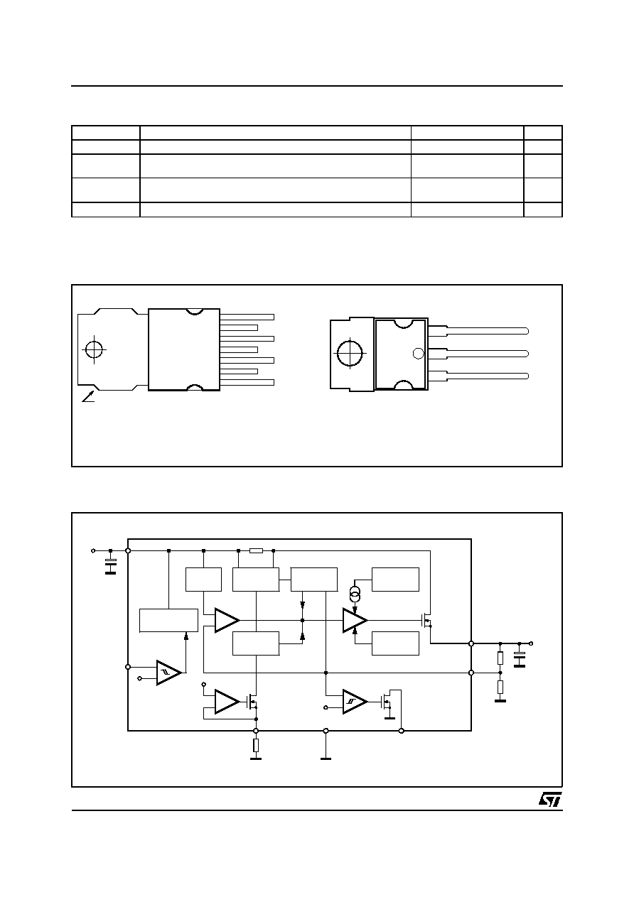
PIN CONNECTIONS (Top views)
HEPTAWATT
1
2
3
4
5
6
7
OUT
PG
ADJ
GND
INH
CL
IN
D96IN367
tab connected to pin 4
OUT
GND
IN
1
3
D96IN369
IN
PROGRAM.
C.L.
PRE
REGULATOR
V
REF
=
1.26V
+
-
E/A
OUT
ADJ
GND
PG
CL
D96IN366
1(1)
3
2
6
4(2)
5
7(3)
PIN x = HEPTAWATT
PIN (x) = VERSAWATT
INHIBIT
ACTIVE HIGH
1.26V
INH
V
IN
10
µ
F
FIXED
C.L.
THERMAL
SHUTDOWN
FOLDBACK
BUFFER
CHARGE
PUMP
POWER
DMOS
150m
+
-
V
REF
+
-
0.9V
REF
R1
22
µ
F
R2
V
OUT
R
CL
(ºW, 1%)
BLOCK DIAGRAM
L4955
2/14

L4955 - ELECTRICAL CHARACTERISTICS (T
j
= 25∞C, V
in
= 12V, unless otherwise specified).
∑
= Specifications referred to T
J
from 0∞C to +125∞C.
Symbol
Parameter
Test Condition
Min.
Typ.
Max.
Unit
V
IN
Operating Supply Voltage
4.5
22
V
V
O
Output Voltage (1)
0.1A < I
O
< 5A; 4.5V < V
IN
<12V
1.235
1.26
1.285
V
4.5V < V
IN
< 12V; 0.1A < I
O
< 5A
∑
1.222
1.26
1.298
V
V
O
Line regulation (1)
4.5V < V
IN
<22V; I
O
= 10mA
2
10
mV
V
O
Load regulation (1)
0.1A < IO < 5A
2
10
mV
V
O
Dropout Voltage
I
O
= 5A
V
IN
4.5V
0.75
1.1
V
∑
1.1
1.5
V
I
O
= 2A
∑
0.55
0.75
V
I
O
Current Limiting
∑
5.1
6.3
7.5
A
Short Circuit Current
V
O
= 0V
∑
1.8
A
Programmable Current
Limiting
R
lim
= 13k
R
lim
= 47k
∑
∑
2.55
0.70
3
0.85
3.45
1.00
A
A
I
Q
Quiescent Current
0.1A < I
O
< 5A C
L
= 0
C
L
= 13k
2
2.7
3
4
mA
mA
Stand By Current
INH = 5V
120
200
µ
A
Inhibit Threshold
Rising Edge
∑
1.1
1.26
1.42
V
Inhibit Hysteresis
0.2
V
Inhibit Bias Sink Current
INH = 5V or 0.8V
20
60
µ
A
Power Good Threshold
Rising Edge
0.9 x V
O
V
Power Good Hysteresis
∑
0.2
V
Power Good Saturation
I
PG
= 4mA
∑
0.1
0.4
V
Ripple Rejection
f = 120Hz, I
O
= 5A
V
IN
= 6V
V
IN
= 2V
PP
60
75
dB
(1) Output voltage connected to ADJ.
THERMAL DATA (HEPTAWATT & VERSAWATT packages)
Symbol
Parameter
Value
Unit
R
th j-case
Thermal Resistance Junction-case Max.
2.5
∞C/W
R
th j-amb
Thermal Resistance Junction-ambient Max.
50
∞C/W
Thermal Shutdown Typ.
150
∞C
Thermal Hysteresis Typ.
20
∞C
PIN FUNCTIONS
HW
VW
Name
Function
1
1
IN
Unregulated input voltage; this pin must be bypassed with a capacitor larger than 10
µ
F.
2
≠
CL
A resistor connected between this pin and ground sets the programmable current limiting
value. When the programmable current limiting is not used the pin must be connected to GND.
3
≠
INH
TTL-CMOS input. A logic high level on this input disables the device. An internal pull-down
insures full functionally even if the pin is open.
4
2
GND
Ground.
5
≠
ADJ
The output is connected directly to this terminal for 1.26V operation; it is connected to the
output through a resistive divider for higher voltages.
6
≠
PG
Open drain output, this signal is low when the output voltage is lower than 90%, otherwise is high.
7
3
OUT
Regulated output voltage. A minimum bypass capacitor of 22
µ
F is required to insure stability.
L4955
3/14
L4955V5.1 - ELECTRICAL CHARACTERISTICS (T
j
= 25∞C, V
in
= 8V, unless otherwise specified)
∑
= Specifications referred to T
J
from 0∞C to +125∞C.
Symbol
Parameter
Test Condition
Min.
Typ.
Max.
Unit
V
IN
Operating Input Voltage
V
O
+V
D
22
V
V
O
Output Voltage
6.75V < V
IN
< 15V; 0.1A < I
O
< 5A
5.000
5.100
5.200
V
6.75V < V
IN
< 15V; 0.1A < I
O
< 5A
∑
4.950
5.100
5.250
V
V
D
Drop-out Voltage
I
O
= 5A
0.75
1.1
V
∑
1.1
1.5
V
I
O
= 2A
∑
0.55
0.75
V
V
O
Line regulation
6.5V < V
IN
<15V; I
O
= 10mA
2
10
mV
V
O
Load regulation
0.1A < IO < 5A
5
20
mV
I
O
Current Limiting
∑
5.1
6.3
7.5
A
Short Circuit Current
V
O
= 0V
∑
1.8
A
I
Q
Quiescent Current
0.1A < I
O
< 5A
2
3
mA
Ripple Rejection
f = 120Hz, I
O
= 5A
V
IN
= 8V
V
IN
= 2V
PP
55
65
dB
L4955V3.3 - ELECTRICAL CHARACTERISTICS (T
j
= 25∞C, V
in
= 5V, unless otherwise specified)
∑
= Specifications referred to T
J
from 0∞C to +125∞C.
Symbol
Parameter
Test Condition
Min.
Typ.
Max.
Unit
V
IN
Operating Input Voltage
4.5
22
V
V
O
Output Voltage
4.75V < V
IN
< 12V; 0.1A < I
O
< 5A
3.234
3.300
3.366
V
4.75V < V
IN
< 12V; 0.1A < I
O
< 5A
∑
3.201
3.300
3.399
V
V
O
Line regulation
4.5V < V
IN
<12V; I
O
= 10mA
2
10
mV
V
O
Load regulation
0.1A < IO < 5A
3
15
mV
I
O
Current Limiting
∑
5.1
6.3
7.5
A
Short Circuit Current
V
O
= 0V
∑
1.8
A
I
Q
Quiescent Current
0.1A < I
O
< 5A
2
3
mA
Ripple Rejection
f = 120Hz, I
O
= 5A
V
IN
= 6V
V
IN
= 2V
PP
57
70
dB
L4955
4/14
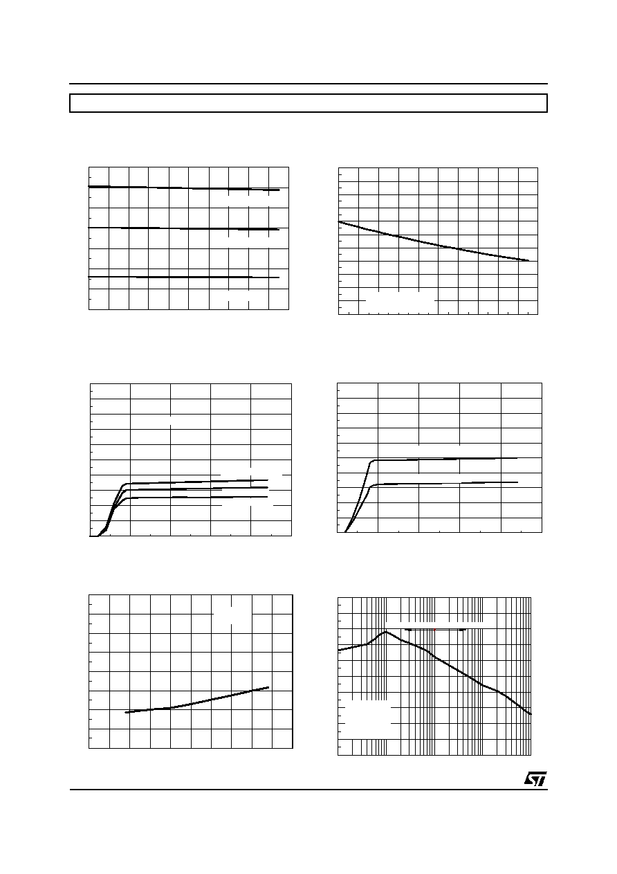
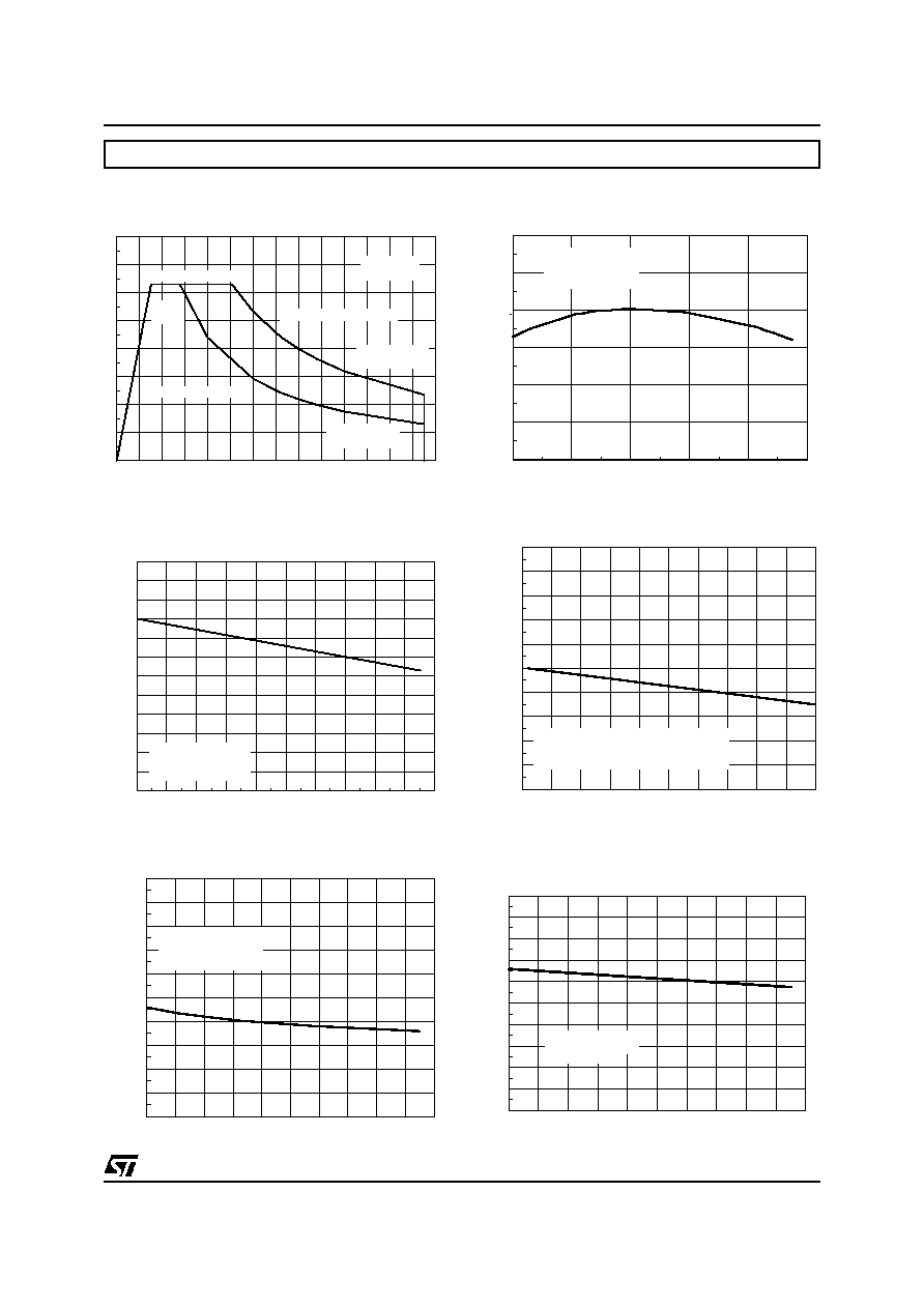
- 4 0
0
4 0
8 0
1 2 0
1 6 0
1 .2 4
1 .2 4 5
1 .2 5
1 .2 5 5
1 .2 6
1 .2 6 5
1 .2 7
1 .2 7 5
1 .2 8
T j [∞ C ]
Vo u t [V ]
V i n = 1 2 V
I o u t= 1 0 m A
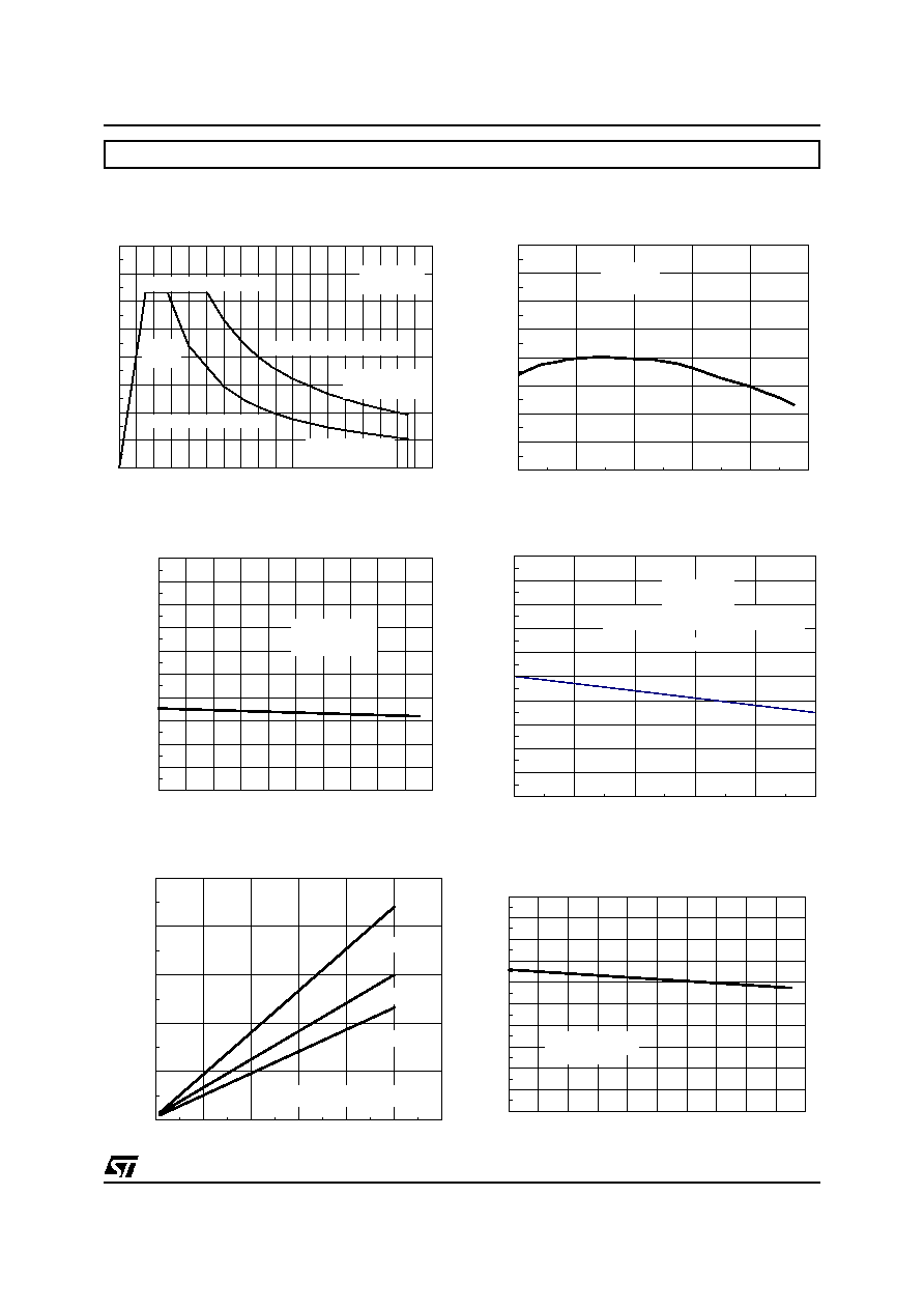
Figure 2: Output Voltage Stability vs. Junction
Temperature
-4 0 -2 0
0
2 0
4 0
6 0
8 0 1 0 0 1 2 0 1 4 0 1 6 0
0
0 .5
1
1 .5
2
2 .5
3
3 .5
4
4 .5
5
T j [∞C ]
O
u
t
put
V
o
l
t
age D
e
v
i
at
i
on [
m
V
]
4 .5 V < V in < 2 2 V
Io u t= 1 0 m A
Figure 3: Line Regulation vs. Junction
Temperature
0
1
2
3
4
5
- 5
- 4
- 3
- 2
- 1
0
1
2
3
4
5
Io u t [A ]
O
u
t
p
u
t
V
o
l
t
ag
e D
e
v
i
at
i
on [
m
V
]
V in = 1 2 V
T j = 2 5 ∞ C
( P u ls e d te c h n iq u e h a s b e e n u s e d )
V o u t = V
A D J
Figure 4: Load Regulation
0
2.5
5
7.5
10
12.5
15
17.5
20
22.5
0
1
2
3
4
5
6
7
8
(V in - Vou t) [V ]
O u tp ut C urrent [A ]
V in > 4.5V
T j = 125∞C
Pow er D issipation L im it
T c = 25∞C
P dm ax = 40W
C urrent Lim itation
T c = 70∞C
P dm ax = 22W
D C O p erating A re a
R dson
lim it
Figure 1: L4955 DC Operating Area
0
1
2
3
4
5
6
0
0 . 2 5
0 . 5
0 . 7 5
1
1 . 2 5
I o u t [ A ]
M
i
n
i
m
u
m
Vi
n
-
V
o
ut
V
o
l
t
age
[
V
]
T j = 1 2 5 ∞ C
T j = 2 5 ∞ C
T j = - 4 0 ∞ C
P u l s e d te c h n i q u e h a s b e e n u s e d
Figure 5: Dropout Voltage
*P ulsed tecnique has been used
-40
-20
0
20
40
60
80
100 120 140 160
0
1
2
3
4
5
6
7
8
9
10
Tj [∞C]
O utput C urre nt [A]
(Vin-Vout) > 2V
pin 2 = G ND
Figure 6: Maximum Output Current vs. Junction
Temperature with internal current limiting
L4955
L4955
5/14
- 4 0 - 2 0
0
2 0
4 0
6 0
8 0 1 0 0 1 2 0 1 4 0 1 6 0
0 . 4
0 . 6
0 . 8
1
1 . 2
1 . 4
1 . 6
1 . 8
2
2 . 2
2 . 4
2 . 6
T j [∞ C ]
I q [ m A ]
V i n = 1 2 V
Io u t= 1 0 m A t o 5 A
Figure 8: Quiescent Current vs. Temperature
(CL = 0V)
1 k
1 0
1 0 0
1 0 k
1 0 0 k
0
1 0
2 0
3 0
4 0
5 0
6 0
7 0
8 0
9 0
1 0 0
F r e q u e n c y [ H z ]
R i p p le R e je c t i o n [ d B ]
C in = 2 2 u F
C o u t = 2 2 u F
V o u t = 1 . 2 6 V
V in m i n = 4 . 5 V
I o u t = 5 A
V r ip p le = 3 V p - p
V r ip p le = 0 . 5 V p - p
Figure 12: Ripple Rejection vs. Frequency
* P u ls e d te c n iq u e h a s b e e n u s e d
- 4 0
- 2 0
0
2 0
4 0
6 0
8 0
1 0 0 1 2 0 1 4 0 1 6 0
0
0 .5
1
1 .5
2
2 .5
3
3 .5
T j [∞ C ]
S h o r t- c ir c u it C u r r e n t [A ]
R lim = 4 7 k
R lim = 1 3 k
R lim = 1 9 k
Figure 7: Short-circuit Current vs. Junction
Temperature with Programmable
Current Limiting
0
5
1 0
1 5
2 0
2 5
0
0 . 5
1
1 . 5
2
2 . 5
3
3 . 5
4
4 . 5
5
V i n [ V ]
I q [ m A ]
I o = 1 0 m A t o 5 A
T j = 2 5 ∞ C
T j = 1 2 5 ∞ C
T j = - 4 0 ∞ C
Figure 9: Quiescent Current vs. Supply voltage
(CL = 0V)
Tj = 25∞C
0
5
10
15
20
25
0
0.5
1
1.5
2
2.5
3
3.5
4
4.5
5
Vin [V]
Iq [mA]
Rlim = 13k
Rlim = 47k
Figure 10: Quiescent Current vs. Supply Voltage
with Programmable Current Limiting
0
5
1 0
1 5
2 0
2 5
0
5 0
1 0 0
1 5 0
2 0 0
2 5 0
3 0 0
3 5 0
4 0 0
V in [V ]
Iq [u A ]
T j= 2 5 ∞ C
Figure 11: Stand-by Current vs. Supply Voltage
with INH = LOGIC HIGH
L4955
L4955
6/14
PG
V
ADJ
0.9 V
ADJ
hyst = 200mV
High
Low
Low
t
t
D96IN364B
V
OUT
=V
ADJ
(R1+R2)/R2
Figure 14: Power Good Function
V
INH
Vref = 1.26V
hyst = 200mV
regulator
OFF
t
t
regulator
ON
regulator
ON
D96IN365A
Figure 15: Inhibit Function
0
1
2
3
4
5
0
1 0
2 0
3 0
4 0
5 0
6 0
7 0
8 0
9 0
1 0 0
I o u t [ A ]
R i p p l e R e j e c t i o n [ d B ]
F r ip p le = 1 2 0 H z
V r i p p l e = 3 V p - p
F r ip p le = 1 0 k H z
V r i p p l e = 0 . 5 V p - p
F r ip p le = 1 k H z
V r i p p l e = 0 . 5 V p - p
F r ip p le = 5 0 k H z
V r i p p l e = 0 . 5 V p - p
C in = 2 2 u F
C o u t = 2 2 u F
V o u t = 1 . 2 6 V
V in m in = 4 . 5 V
Figure 13: Ripple Rejection vs. Output Current
L4955
L4955
7/14
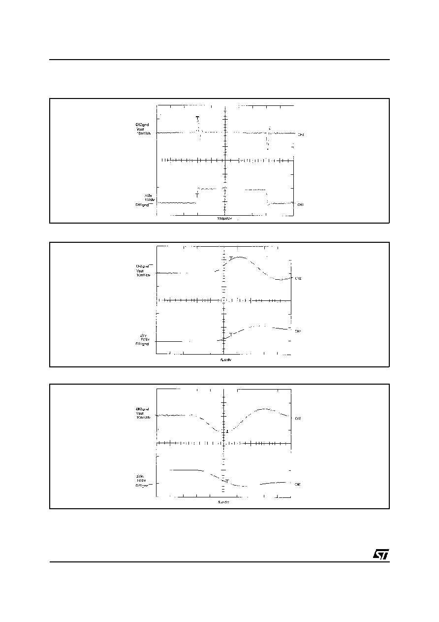
LINE TRANSIENT RESPONSE
Figure 16.
Figure 17.
Figure 18.
Test condition: V
IN
= 12V;
V
IN
= 1V; V
O
= 3.3V; I
O
= 200mA; C
IN
= 10
µ
F (electrolytic capacitor);
C
out
= 22
µ
F (electrolytic capacitor); dV/dt = 0.1 V/
µ
s; T
J
= 25∞C
L4955
8/14
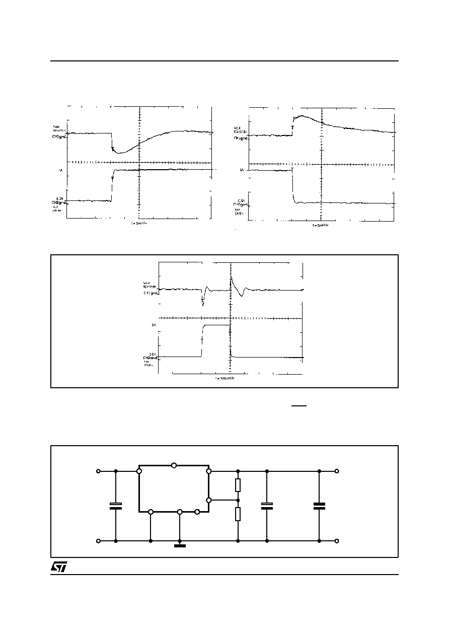
LOAD TRANSIENT RESPONSE
Figure 19.
Figure 20.
Figure 21.
C1,C2
470
µ
F/25V
Panasonic
HFQ
R4
910
R5
560
C4 to C9
100
µ
F/10V
AVX TPS
6 each
C10 to C15
1
µ
F
AVX X7R
6 each
VOUT = 3.3V
VIN = 5V
1
2
IN
CL
GND
4
3
INH
7
OUT
5
ADJ
L4955
PG
6
D97IN546
Figure 22: Load transient test circuit.
Test condition: V
IN
= 5V, V
OUT
= 3.3V; Load Transient from 0.5A to 5A;
dI
out
dt
=
20A
/
µ
s
; T
J
= 25∞C
L4955
9/14

L4955V3.3
3
4.5
6
7.5
9
10.5 12 13.5 15 16.5 18 19.5 21 22.5
0
1
2
3
4
5
6
7
8
Input Voltage [V]
O utput C urrent [A]
C urrent Lim itation
Vo ut = 3.3V
Tj = 125∞C
Pow er D issipation Lim it
Tc = 25∞C
Pdm ax=40W
R ds on
lim it
D C O peratin g Area
Tc =70∞C
Pdm ax=22W
Figure 23: DC operating area.
-4 0
0
4 0
8 0
1 20
1 60
3 .2
3 .25
3 .3
3 .35
3 .4
T j [∞C ]
Vo ut [V]
Vin = 5V
Iou t = 1 0m A
Figure 24: Output Voltage Stability vs. Junction
Temperature.
-4 0
-2 0
0
2 0
4 0
6 0
8 0
1 0 0
1 2 0
1 4 0
1 6 0
0
0 .2 5
0 .5
0 .7 5
1
1 .2 5
1 .5
1 .7 5
2
2 .2 5
2 .5
2 .7 5
3
T j [∞C ]
Iq [m A ]
V in = 5 V
Io u t = 1 0 m A to 5 A
Figure 25: Quiescent Current vs. Temperature.
0
1
2
3
4
5
-5
-4
-3
-2
-1
0
1
2
3
4
5
Iout [A]
O
u
t
p
u
t
V
o
l
t
ag
e D
e
v
i
at
i
on [
m
V
]
Vin=5V
Tj = 25 ∞C
(Pulsed tecnique has been used)
Figure 26: Load Regulation
-40
-2 0
0
20
40
60
80
100
120
140
160
0
0.5
1
1.5
2
2.5
3
3.5
4
4.5
5
T j [∞C ]
O
u
t
put
V
o
l
t
age
D
e
v
i
at
i
on
[
m
V
]
4 .5 V < V in < 1 2 V
Io u t = 1 0 m A
Figure 27: Line regulation vs. Junction Tempera-
ture.
*P ulsed tecnique has been used
-40
-20
0
20
40
60
80
100 120 140 160
0
1
2
3
4
5
6
7
8
9
10
Tj [∞C]
O utput C urre nt [A]
(Vin-Vout) > 2V
pin 2 = G ND
Figure 28: Maximum Output Current vs. Junction
Temperature with internal current limiting
L4955
10/14
L4955V5.1
0
2.5
5
7 .5
10
12 .5
15
1 7.5
0
1
2
3
4
5
6
7
8
(V in - Vout) [V ]
O utput C u rre nt [A ]
C urre nt L im itatio n
Vout = 5.1V
T j = 125∞C
Pow er D is s ip atio n Lim it
R d so n
lim it
D C O peratin g A rea
T c = 2 5∞C
P dm a x = 40W
T c = 70 ∞C
P dm a x = 2 2W
Figure 29: DC operating area.
-40
0
40
80
120
160
4.9
4.95
5
5.05
5.1
5.15
5.2
Tj [∞C]
Vout [V]
Vin = 8V
Iout = 10mA
Figure 30: Output Voltage Stability vs. Junction
Temperature.
-40
-20
0
20
40
60
80
100
120
140
160
0
0.25
0.5
0.75
1
1.25
1.5
1.75
2
2.25
2.5
2.75
3
Tj [∞C]
Iq [mA]
Vin = 8V
Iout = 10mA to 5A
Figure 31: Quiescent Current vs. Temperature.
0
1
2
3
4
5
-10
-8
-6
-4
-2
0
2
4
6
8
10
Io ut [A]
O
u
t
put
V
o
l
t
age D
e
v
i
at
i
o
n
[
m
V
]
V in = 8 V
T j = 2 5 ∞C
(P u ls e d te c n iq u e h a s b e e n u s e d )
Figure 32: Load Regulation
-40
-20
0
20
40
60
80
100
120
140
160
0
0.5
1
1.5
2
2.5
3
3.5
4
4.5
5
Tj [∞C]
O
u
tput V
o
l
t
age D
e
v
i
at
i
on [m
V
]
6.5V < Vin < 15V
Iout = 10mA
Figure 33: Line regulation vs. Junction Tempera-
ture.
*P ulsed tecnique has been used
-40
-20
0
20
40
60
80
100 120 140 160
0
1
2
3
4
5
6
7
8
9
10
Tj [∞C]
O utput C urre nt [A]
(Vin-Vout) > 2V
pin 2 = G ND
Figure 34: Maximum Output Current vs. Junction
Temperature with internal current limiting
L4955
11/14
Heptawatt V
DIM.
mm
inch
MIN.
TYP.
MAX.
MIN.
TYP.
MAX.
A
4.8
0.189
C
1.37
0.054
D
2.4
2.8
0.094
0.110
D1
1.2
1.35
0.047
0.053
E
0.35
0.55
0.014
0.022
E1
0.7
0.97
0.028
0.038
F
0.6
0.8
0.024
0.031
F1
0.9
0.035
G
2.34
2.54
2.74
0.095
0.100
0.105
G1
4.88
5.08
5.28
0.193
0.200
0.205
G2
7.42
7.62
7.82
0.295
0.300
0.307
H2
10.4
0.409
H3
10.05
10.4
0.396
0.409
L
16.7
16.9
17.1
0.657
0.668
0.673
L1
14.92
0.587
L2
21.24
21.54
21.84
0.386
0.848
0.860
L3
22.27
22.52
22.77
0.877
0.891
0.896
L4
1.29
0.051
L5
2.6
2.8
3
0.102
0.110
0.118
L6
15.1
15.5
15.8
0.594
0.610
0.622
L7
6
6.35
6.6
0.236
0.250
0.260
L9
0.2
0.008
M
2.55
2.8
3.05
0.100
0.110
0.120
M1
4.83
5.08
5.33
0.190
0.200
0.210
V4
40∞ (typ.)
Dia
3.65
3.85
0.144
0.152
A
L
L1
C
D1
L5
L2
L3
D
E
M1
M
H3
Dia.
L7
L6
F1
H2
F
G
G1
G2
E1
F
E
L9
V4
L4
H2
V
V
HEPTAMEC
H1
OUTLINE AND
MECHANICAL DATA
L4955
12/14

Versawatt (TO220)
DIM.
mm
inch
MIN.
TYP.
MAX.
MIN.
TYP.
MAX.
A
4.40
4.60
0.173
0.181
C
1.23
1.32
0.048
0.051
D
2.40
2.72
0.094
0.107
E
0.49
0.70
0.019
0.027
F
0.61
0.88
0.024
0.034
F1
1.14
1.70
0.044
0.067
F2
1.14
1.70
0.044
0.067
G
4.95
5.15
0.194
0.203
G1
2.40
2.70
0.094
0.106
H2
10.0
10.4
0.393
0.409
L2
16.4
0.645
L4
13.0
14.0
0.511
0.551
L5
2.65
2.95
0.104
0.116
L6
15.25
15.75
0.600
0.620
L7
6.20
6.60
0.244
0.260
L9
3.50
3.93
0.137
0.154
M
2.6
0.102
Dia
3.75
3.85
0.147
0.151
M
TO220MEC
OUTLINE AND
MECHANICAL DATA
L4955
13/14

Information furnished is believed to be accurate and reliable. However, STMicroelectronics assumes no responsibility for the consequences
of use of such information nor for any infringement of patents or other rights of third parties which may result from its use. No license is
granted by implication or otherwise under any patent or patent rights of STMicroelectronics. Specification mentioned in this publication are
subject to change without notice. This publication supersedes and replaces all information previously supplied. STMicroelectronics products
are not authorized for use as critical components in life support devices or systems without express written approval of STMicroelectronics.
The ST logo is a registered trademark of STMicroelectronics
© 1999 STMicroelectronics ≠ Printed in Italy ≠ All Rights Reserved
STMicroelectronics GROUP OF COMPANIES
Australia - Brazil - Canada - China - France - Germany - Italy - Japan - Korea - Malaysia - Malta - Mexico - Morocco - The Netherlands -
Singapore - Spain - Sweden - Switzerland - Taiwan - Thailand - United Kingdom - U.S.A.
http://www.st.com
L4955
14/14