 | –≠–ª–µ–∫—Ç—Ä–æ–Ω–Ω—ã–π –∫–æ–º–ø–æ–Ω–µ–Ω—Ç: L4956 | –°–∫–∞—á–∞—Ç—å:  PDF PDF  ZIP ZIP |
L4956
5A LOW DROP LINEAR REGULATOR
SPLITTED SUPPLY VOLTAGE FOR IM-
PROVED EFFICIENCY:
- V
PW
: 3V MIN. POWER SUPPLY VOLTAGE
- V
SIG
: 4.5V MIN. SIGNAL SUPPLY VOLTAGE
5A OUTPUT CURRENT
FAST LOAD TRANSIENT RESPONSE
0.75V TYP. DROP OUT VOLTAGE AT 5A
INHIBIT WITH ZEROCURRENT COMSUMPTION
POWER GOOD
SHORT CIRCUIT PROTECTION
THERMAL SHUTDOWN
HEPTAWATT PACKAGE
APPLICATIONS
PENTIUM
TM
AND POWER PC
TM
SUPPLIES
LOW COST SOLUTION FOR 3.3V TO 1.5V
CONVERSION
SUITABLE
FOR
APPLICATIONS
WITH
STAND BY FEATURE
DESCRIPTION
The L4956 is an adjustable monolithic linear regu-
lator designed to satisfy very heavy load transient
and efficient power conversion from 3.3V to 1.26V
and lower, up to 5A.
Designed in BCDII technology, it uses a charge
pump technique to have a proper internal N-chan-
nel gate drive. The signal supply voltage input
V
SIG
can operate from 4.5V up to an absolute of
7V and the power supply voltage input V
PW
can
opearte from 3V min to an absolute of 7V. An
RDSON of 150mV gives a voltage drop of 750mV
at 5A of load current.
Very fast load transients and
±
1% of reference
voltage precision makes this device suitable for
supplying last micrprocessors generation and low
voltage logics.
The Heptawatt package enriches the device with
auxiliary functions like power good and inhibit.
March 1998
HEPTAWATT
ORDERING NUMBER: L4956
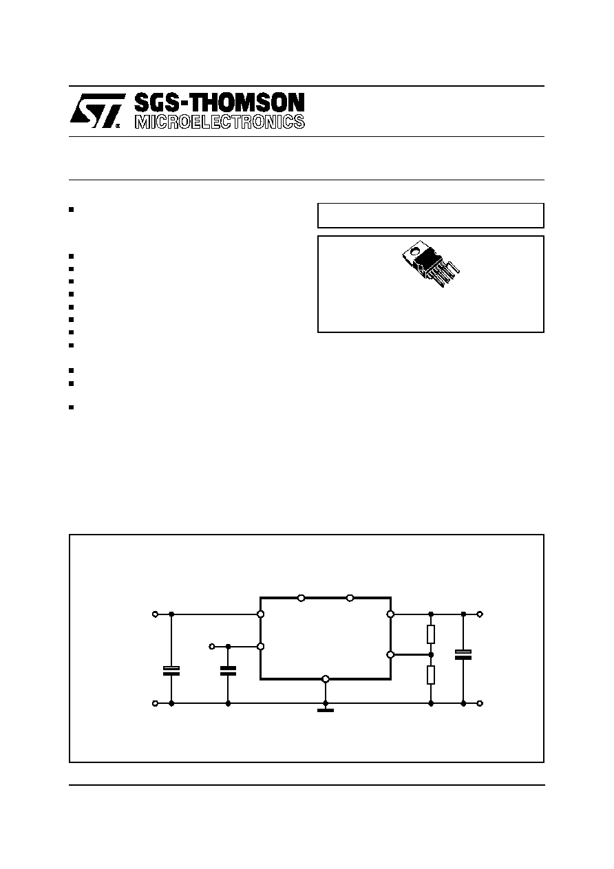
MULTIPOWER BCD TECHNOLOGY
V
PW
V
SIG
D96IN374B
1
2
7
OUT
5
ADJ
4
GND
L4956
C
1
R
1
R
2
C
2
V
O
V
PW
=3.3Vbus
V
SIG
=
5Vbus
3
6
INH
PG
C
3
TYPICAL APPLICATION
1/8
ABSOLUTE MAXIMUM RATINGS
Symbol
Parameter
Value
Unit
V
PW
, V
SIG
Supply Input Voltage
7
V
ADJ pin
PG and INH pins
-0.3 to 4
0 to V
SIG
V
V
P
TOT
Power Dissipation @ T
amb
= 50
∞
C
Power Dissipation @ T
case
= 90
∞
C
2
15
W
W
T
st
, T
i
Storage Temperature
-40 to +150
∞
C
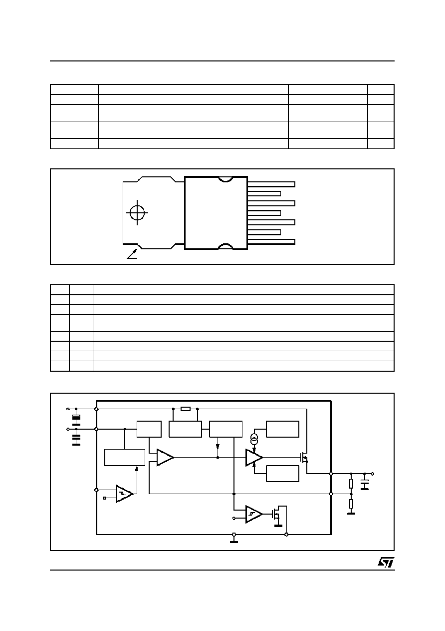
PIN FUNCTIONS
No.
Name
Function
1
V
PW
Unregulated power input voltage; this pin must be bypassed with a capacitor larger than 10
µ
F.
2
V
SIG
Unregulated signal input voltage this pin has to be by passed with a minimum capacitor of 0.1
µ
F.
3
INH
TTL-CMOS input. A logic level on this input disable the device. An internal pull-down insures insures
full functionally even if the pin is open.
4
GND
Ground.
5
ADJ
The output is connected directly to this terminal for 1.26V operation via divider for higher voltages.
6
PG
Open drain output, this pin is low when the output voltage is lower than 90%, otherwise is high.
7
OUT
Regulated output voltage. A minimum bypass capacitor of 22
µ
F is required to insure stability.
1
2
3
4
5
6
7
OUT
PG
ADJ
GND
INH
V
SIG
V
PW
D96IN373
tab connected to pin 4
PIN CONNECTION (Top view)
V
PW
PRE
REGULATOR
V
REF
=
1.26V
+
-
E/A
OUT
ADJ
GND
PG
D96IN372A
1
3
6
4
5
7
INHIBIT
ACTIVE HIGH
1.26V
INH
V
PW
10
µ
F
CURRENT
LIMITATION
THERMAL
SHUTDOWN
FOLDBACK
BUFFER
CHARGE
PUMP
POWER
DMOS
150m
+
-
0.9V
REF
R1
22
µ
F
R2
V
OUT
V
SIG
2
V
SIG
BLOCK DIAGRAM
L4956
2/8
ELECTRICAL CHARACTERISTICS (T
j
= 25
∞
C, unless otherwise specified)
Symbol
Parameter
Test Condition
Min.
Typ.
Max.
Unit
V
PW
Power Operating Supply Voltage
3
6.5
V
V
SIG
Signal Operating Supply Voltage
4.5
6.5
V
V
OUT
Output Voltage
(1)
0 < Tj < 125
∞
C; V
PW
= 3.3V
4.5V < V
SIG
< 6.5V; 0.1A < I
O
< 5A
1.240
1.260
1.280
V
3V < V
PW
< 5.5V; 4.5V< V
SIG
< 6.5V
0.1A < I
O
< 5A; 0 < T
j
< 125
∞
C
1.224
1.260
1.296
V
V
OUT
Line regulation
(1)
3V < V
PW
< 5.5V; I
O
= 10mA
4.5V < V
SIG
< 6.5V
0.5
3
mV
V
OUT
Load regulation (1)
VPW = 3.3V; V
SIG
= 5V
0.1A < I
O
< 5A
1
5
mV
Drop-out Voltage
I
O
= 5A
I
O
= 5A, T
j
= 125
∞
C
0.75
1.1
1.1
1.5
V
V
I
O
Current Limiting
0 < T
j
< 125
∞
C
5.1
6.3
7.5
A
Short Circuit Current
V
O
= 0V, 0 < T
j
< 125
∞
C
1.8
A
I
Q
Quiescent Current at pin V
SIG
0.1A < I
O
< 5A
4.5V < V
SIG
<6.5V
1.5
3
mA
Stand By Current at pin V
SIG
INH = HIGH V
SIG
= 5V
100
150
µ
A
Inhibit Threshold
0 < Tj < 125
∞
C
1.1
1.26
1.42
V
Inhibit Histeresys
0.2
V
Inhibit Bias Sink Current
5
10
µ
A
Power Good Threshold
0.9 x
V
OUT
V
Power Good Saturation
I
6
= 4mA
0.1
0.4
V
Power Good Histeresys
0.2
V
(1) Output voltage connected to ADJ.
THERMAL DATA
Symbol
Parameter
Value
Unit
R
th j-pins
Thermal Resistance Junction-case
2.5
∞
C/W
R
th j-amb
Thermal Resistance Junction-ambient
50
∞
C/W
Thermal Shutdown
Typ.
150
∞
C
Thermal Hysteresis
Typ.
20
∞
C
L4956
3/8
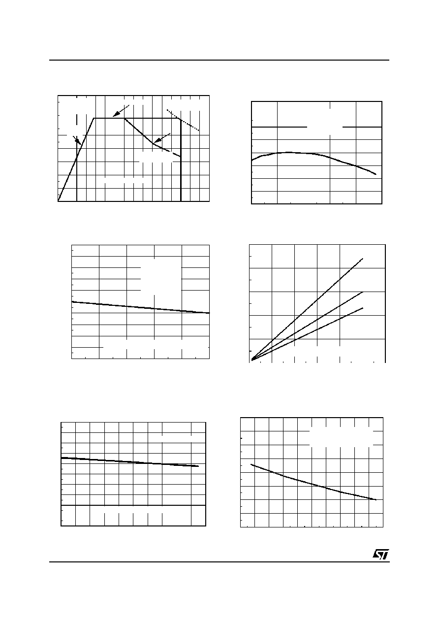
P ow e r
D issip a tio n
L im it
0
1
2
3
4
5
6
7
8
0
1
2
3
4
5
6
7
8
(V p w - Vo u t) [V ]
O u tpu t C urre n t [A ]
V pw > 3V
V s ig > 4.5 V
T j = 1 25
∞
C
Tc = 2 5
∞
C
P dm ax = 4 0 W
C u rre nt Lim ita ti o n
R d s on
lim it
D C O p e ra ting A rea
Tc = 7 0
∞
C
P dm ax =2 2 W
Figure 1. DC Operating Area.
-40
0
4 0
8 0
12 0
1 6 0
1 .2 4
1 .2 4 5
1 .2 5
1 .2 5 5
1 .2 6
1 .2 6 5
1 .2 7
1 .2 7 5
1 .2 8
T j [
∞
C ]
Vo ut [V ]
V p w = 3 .3 V
V sig = 5 V
I o u t = 1 0 m A
Figure 2. Output Voltage Stability vs.
Junction Temperature
0
1
2
3
4
5
-5
-4
-3
-2
-1
0
1
2
3
4
5
I ou t [A ]
O
utput
Voltage
Deviation
[m
P u ls e d t e c n iq u e h a s b e e n u s e d
V p w = 3 . 3 V
V s i g = 5 V
Vo u t = Va d j
T j = 2 5
∞
C
Figure 3. Load Regulation.
0
1
2
3
4
5
6
0
0 .2 5
0 .5
0 .7 5
1
1 .2 5
Io u t [A ]
Minimum
Vpw
-
Vout
Voltage
[V]
T j = 1 2 5
∞
C
T j = 2 5
∞
C
T j = - 4 0
∞
C
P u ls ed te c hn iq u e h a s b e e n u s e d
Figure 4. Dropout Voltage.
-4 0 -20
0
20
4 0
6 0
8 0 10 0 12 0 1 40 1 60
0
1
2
3
4
5
6
7
8
9
1 0
Tj [∫C ]
O u tp u t C u rre nt [A ]
(V p w -Vo u t) > 2 V
P u ls e d te cn iq u e h a s b e e n u s e d
Figure 5. Maximum Output Current vs.
Junction Temperature
- 4 0
- 2 0
0
2 0
4 0
6 0
8 0
1 0 0 1 2 0 1 4 0 1 6 0
0 .4
0 .6
0 .8
1
1 .2
1 .4
1 .6
1 .8
2
T j [
∞
C ]
I q [m A ]
V
S IG
= 6 . 5 V
I o u t = 1 0 m A to 5 A
3 V < V P W < 6 .5 V
Figure 6. Quiescent Current at pin VSIG vs.
Junction Temperature.
L4956
4/8
0
1
2
3
4
5
6
7
0
0 . 5
1
1 . 5
2
2 . 5
3
V S I G [ V ]
I q [ m A ]
I o = 1 0 m A
t o
5 A
T j = 2 5
∞
C
3 V < V P W < 6 . 5 V
Figure 7. Quiescent Current at pin VSIG vs.
Signal Input Voltage.
4
4 . 5
5
5 . 5
6
6 . 5
7
0
2 5
5 0
7 5
1 0 0
1 2 5
1 5 0
V S I G [ V ]
I q [
µ
A ]
T j = 2 5
∞
C
3 V < V P W < 6 . 5 V
Figure 8. Stand-By Current at pin VSIG vs. Signal
Input Voltage with INH = LOGIC HIGH
PG
V
ADJ
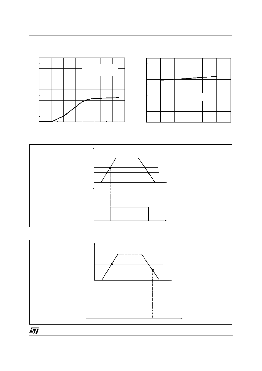
0.9 V
ADJ
hyst = 200mV
High
Low
Low
t
t
D96IN364B
V
OUT
=V
ADJ
(R1+R2)/R2
Figure 9. Power Good Function
V
INH
Vref = 1.26V
hyst = 200mV
regulator
OFF
t
t
regulator
ON
regulator
ON
D96IN365A
Figure 10. Inhibit Function
L4956
5/8
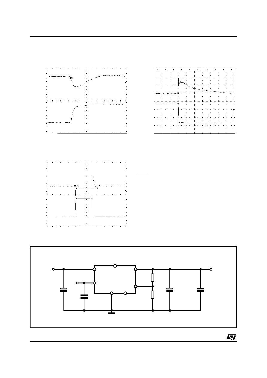
LOAD TRANSIENT RESPONSE
Figure 11.
Vout
50mV/div
CH1gnd
5A
0.5A
CH2gnd
Iout
2A/div
t = 5
µ
s/div
Figure 12.
Vout
50mV/div
CH1gnd
5A
t = 5
µ
s/div
Figure 13.
Vout
50mV/div
CH1gnd
5A
t = 100
µ
s/div
0.5A
CH2gnd
Iout
2A/div
0.5A
CH2gnd
Iout
2A/div
C1,C2
470
µ
F
Panasonic
HFQ
R4
24
R5
126
C4 to C9
100
µ
F/10V
AVX TPS
6 each
C10 to C15
1
µ
F
AVX X7R
6 each
VOUT=1.5V
VIN=3.3V
1
V
PW
GND
4
3
INH
7
OUT
5
ADJ
L4956
PG
6
D97IN593
V
SIG
C16
220nF
V
SIG
=5V
2
Figure 14. Load transient test circuit.
Test conditions:
V
PW
= 3.3V; V
SIG
= 5; V
out
= 1.5V; Load Transient
from 0.5A to 5A;
dl
out
dt
= 20A/
µ
s; Tj = 25
∞
C
L4956
6/8
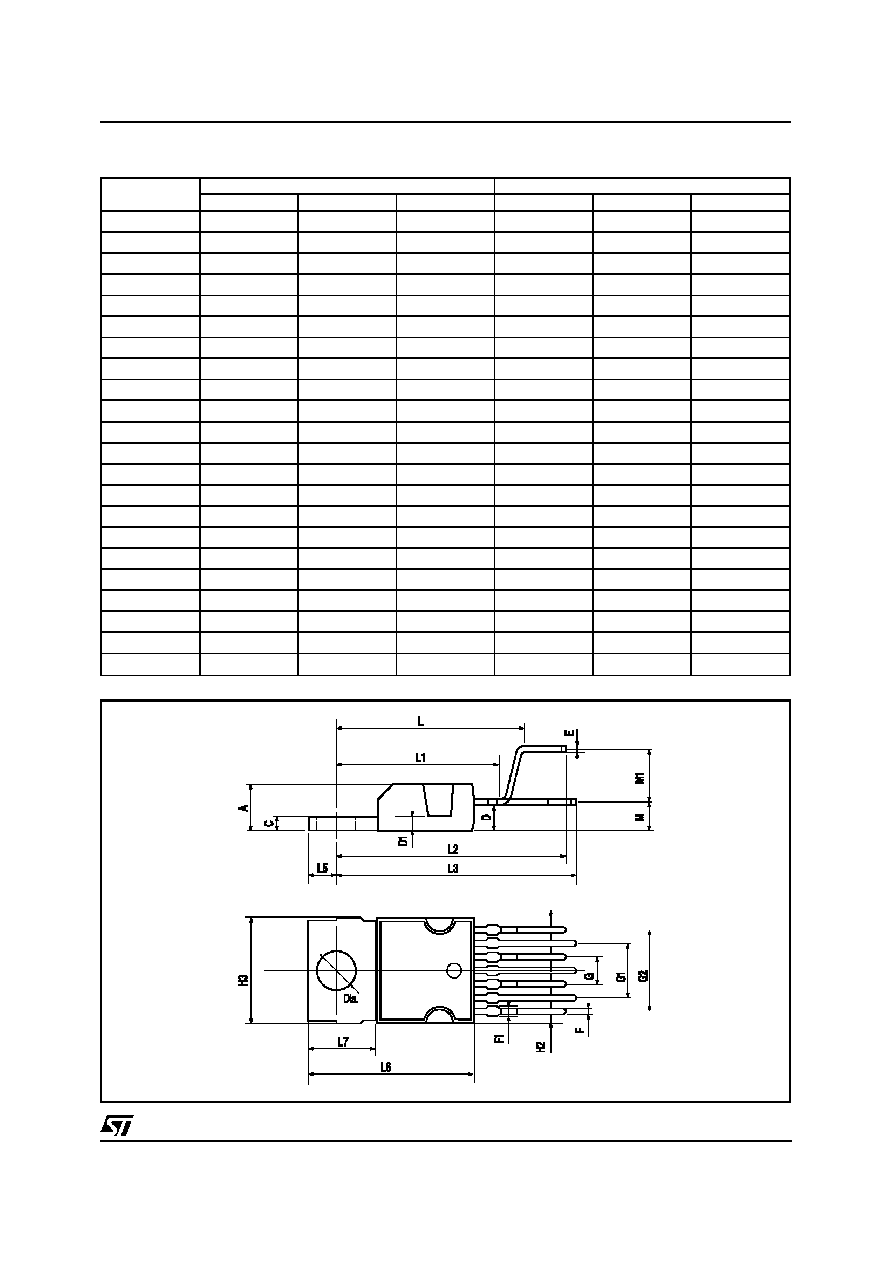
HEPTAWATT PACKAGE MECHANICAL DATA
DIM.
mm
inch
MIN.
TYP.
MAX.
MIN.
TYP.
MAX.
A
4.8
0.189
C
1.37
0.054
D
2.4
2.8
0.094
0.110
D1
1.2
1.35
0.047
0.053
E
0.35
0.55
0.014
0.022
F
0.6
0.8
0.024
0.031
F1
0.9
0.035
G
2.41
2.54
2.67
0.095
0.100
0.105
G1
4.91
5.08
5.21
0.193
0.200
0.205
G2
7.49
7.62
7.8
0.295
0.300
0.307
H2
10.4
0.409
H3
10.05
10.4
0.396
0.409
L
16.97
0.668
L1
14.92
0.587
L2
21.54
0.848
L3
22.62
0.891
L5
2.6
3
0.102
0.118
L6
15.1
15.8
0.594
0.622
L7
6
6.6
0.236
0.260
M
2.8
0.110
M1
5.08
0.200
Dia
3.65
3.85
0.144
0.152
L4956
7/8

Information furnished is believed to be accurate and reliable. However, SGS-THOMSON Microelectronics assumes no responsibility for the
consequences of use of such information nor for any infringement of patents or other rights of third parties which may result from its use. No
license is granted by implication or otherwise under any patent or patent rights of SGS-THOMSON Microelectronics. Specification mentioned
in this publication are subject to change without notice. This publication supersedes and replaces all information previously supplied. SGS-
THOMSON Microelectronics products are not authorized for use as critical components in life support devices or systems without express
written approval of SGS-THOMSON Microelectronics.
©
1998 SGS-THOMSON Microelectronics ≠ Printed in Italy ≠ All Rights Reserved
SGS-THOMSON Microelectronics GROUP OF COMPANIES
Australia - Brazil - Canada - China - France - Germany - Italy - Japan - Korea - Malaysia - Malta - Morocco - The Netherlands -
Singapore - Spain - Sweden - Switzerland - Taiwan - Thailand - United Kingdom - U.S.A.
L4956
8/8