 | –≠–ª–µ–∫—Ç—Ä–æ–Ω–Ω—ã–π –∫–æ–º–ø–æ–Ω–µ–Ω—Ç: L4963D | –°–∫–∞—á–∞—Ç—å:  PDF PDF  ZIP ZIP |

L4963
L4963D
1.5A SWITCHING REGULATOR
Æ
This is advanced information on a new product now in development or underogin evaluation. Details are subject to change without notice.
1.5A OUTPUT LOAD CURRENT
5.1 TO 36V OUTPUT VOLTAGE RANGE
DISCONTINUOUS VARIABLE FREQUENCY
MODE
PRECISE (+/≠2%) ON CHIP REFERENCE
VERY HIGH EFFICIENCY
VERY FEW EXTERNAL COMPONENTS
NO FREQ. COMPENSATION REQUIRED
RESET AND POWER FAIL OUTPUT FOR MI-
CROPROCESSOR
INTERNAL CURRENT LIMITING
THERMAL SHUTDOWN
DESCRIPTION
The L4963 is a monolithic power switching regulator
delivering 1.5A at 5.1V. The output voltage is adjust-
able from 5.1V to 36V, working in discontinuous
variable frequency mode. Features of the device
include remote inhibit, internal current limiting and
thermal protection, reset and power fail outputs for
microprocessor.
BLOCK DIAGRAM
Powerdip12+3+3
SO20
ORDERING NUMBERS:
L4963W
L4963D
The L4963 is mounted in a 12+3+3 lead Powerdip
(L4963) and SO20 large (L4963D) plastic pack-
ages and requires very few external components.
June 2000
1/17
ABSOLUTE MAXIMUM RATINGS
Symbol
Parameter
Value
Unit
SO20
Powerdip
V
i
Input Voltage (pin 1 and pin 3 connected togheter)
47
V
V
3
≠V
2
Input to Output Voltage Difference
47
V
V
2
Negative Output DC Voltage
≠1
V
V
2
Negative Output Peak Voltage at t=0.2
µ
s, f=50kHz
≠5
V
V
8
V
7
Power Fail Input
25
V
V
9
, V
11
V
8
, V
10
Reset and Power Fail Output
V
i
V
10
V
9
Reset Delay Input
5.5
V
V
13
, V
18
V
12
, V
16
Feedback and Inhibit Inputs
7
V
V
19
, V
20
V
17
, V
18
Oscillator Inputs
5.5
V
P
tot
Total Power Dissipation Tpins
90
∞
C (Power DIP)
(T
amb
= 70
∞
C no copper area on PCB)
(T
amb
= 70
∞
C, 4cm
2
copper area on PCB)
5
1.3
2
W
W
W
T
stg
, T
j
Storage & Junction Temperature
(Tamb = 70
∞
C 6cm
2
copper area on PCB)
≠40 to 150
1.45
∞
C
W
P
tot
Total Power Dissipation Tpins
90
∞
C (SO20L)
4
W
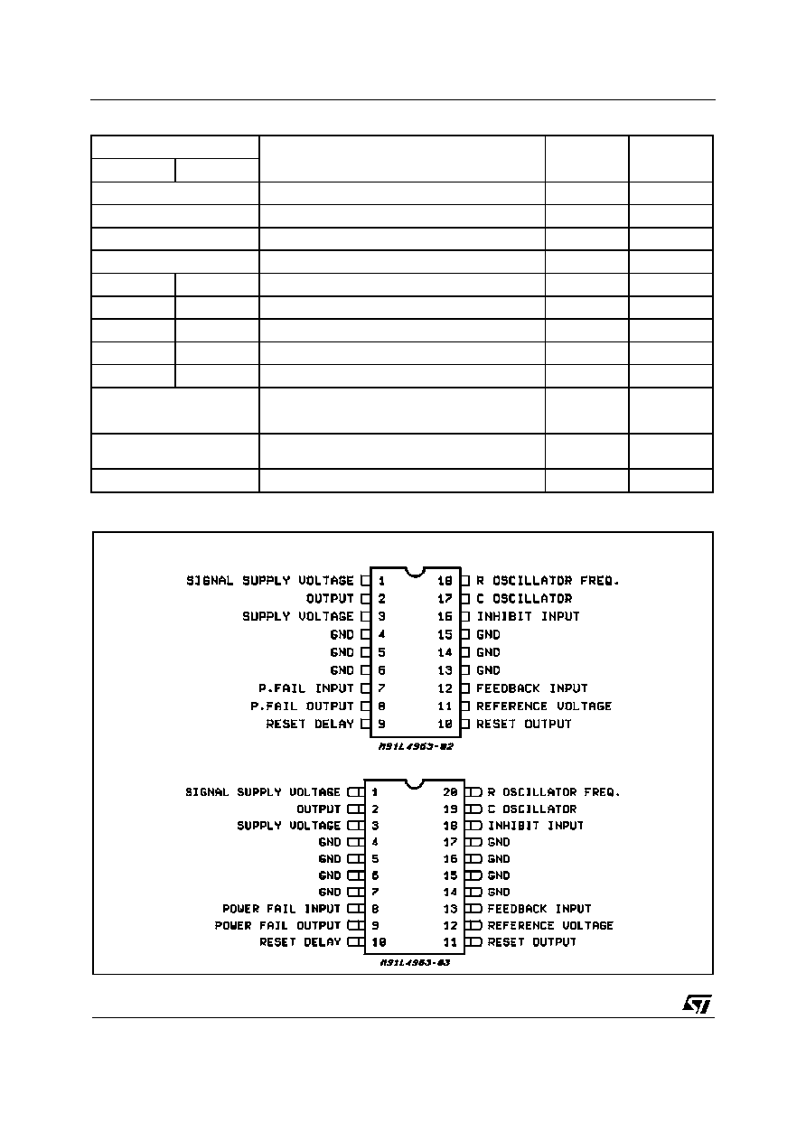
PIN CONNECTION (top view)
Powerdip18
SO20
L4963 - L4963D
2/17

PIN FUNCTIONS
SO20L
Power DIP
Name
Description
1
1
SIGNAL SUPPLY VOLTAGE
Must be Connected to pin 3
2
2
OUTPUT
Regulator output
3
3
SUPPLY VOLTAGE
Unregulated voltage input. An internal regulator
powers the internal logic.
4, 5, 6, 7
14, 15, 16, 17
4, 5, 6
13, 14, 15
GROUND
Common ground terminal
8
7
POWER FAIL INPUT
Input of the power fail circuit. The threshold can be
modified introducing an external voltage divider
between the Supply Voltage and GND.
9
8
POWER FAIL OUTPUT
Open collector power fail signal output. This output
is high when the supply voltage is safe.
10
9
RESET DELAY
A capacitor connected between this terminal and
ground determines the reset signal delay time.
11
10
RESET OUTPUT
Open collector reset signal output. This output is
high when the output voltage value is correct.
12
11
REFERENCE VOLTAGE
Reference voltage output.
13
12
FEEDBACK INPUT
Feedback terminal of the regulation loop.
The output is connected directly to this terminal for
5.1V operation; it is connected via a divider for
higher voltages.
18
16
INHIBIT INPUT
TTL level remote inhibit. A logic low level on this
input disables the device.
19
17
C OSCILLATOR
Oscillator waveform. A capacitor connected
between this terminal and ground modifies the
maximum oscillator frequency.
20
18
R OSCILLATOR FREQ.
A resistor connected between this terminal and
ground defines the maximum switching frequency.
THERMAL DATA
Symbol
Parameter
SO20
Powerdip
Unit
R
th j-pins
Thermal Resistance Junction to Pins
max.
15
12
∞
C/W
R
th j-amb
Thermal Resistance Junction to Ambient (*)
max.
85
80
∞
C/W
(*) See Fig. 28
L4963 - L4963D
3/17

CIRCUIT DESCRIPTION (Refer to Block Dia-
gram)
The L4963 is a monolithic stepdown regulator pro-
viding 1.5A at 5.1V working in discontinuous vari-
able frequency mode. In normal operation the
device resonates at a frequency dependingprimar-
ily on the inductance value, the input and output
voltage and the load current. The maximum switch-
ing however can be limited by an internal oscillator,
which can be programmed by only one external
resistor.
The fondamental regulation loop consists of two
comparators, a precision 5.1V on-chip reference
and a drive latch. Briefly the operation is as follows:
when the choke ends its discharge the catch free-
wheeling recirculation filter diode begins to come
out of forward conduction so the output voltage of
the device approaches ground. When the output
voltage reaches ≠0.1V the internal comparator sets
the latch and the power stage is turned on. Then
the inductor current rises linearly until the voltage
sensed at the feedback input reaches the 5.1V
reference.
The second comparator then resets the latch and
the output stage is turned off. The current in the
choke falls linearly until it is fully discharged, then
the cycle repeats. Closing the loop directly gives an
output voltage of 5.1V. Higher output voltages are
obtained by inserting a voltage divider and this
method of control requires no frequency compen-
sation network. At output voltages greater than
5.1V the available output current must be derated
due to the increased power dissipation of the de-
vice.
Output overload protection is provided by an inter-
nal current limiter. The load current is sensed by a
on-chip metal resistor connected to a comparator
which resets the latch and turns off the power stage
in overload condition. The reset circuits (see fig. 1)
generates an output high signal when the output
voltage value is correct. It has an open collector
output and the output signal delay time can be
programmed with an external capacitor. A power-
fail circuit is also available and is used to monitor
the supply voltage. Its output goes high when the
supply voltage reaches a pre-programmedtreshold
set by a voltage divider to its input from the supply
to ground. With the input left open the threshold is
approximately equal to 5.1V. The output of the
power fail is an open collector.
A TTL level inhibit is provided for applications such
as remote on/off control. This input is activated by
a low logic level and disables circuits operation.
The thermal overload circuit disables the device
when the junction temperature is about 150
∞
C and
has hysteresis to prevent unstable conditions.
Figure 1: Reset and Power Fail Function
L4963 - L4963D
4/17

ELECTRICAL CHARACTERISTIC (Refer to the test circuit V
i
= 30V T
j
= 25
∞
C unless otherwise specified )
Symbol
Parameter
Test Conditions
Min.
Typ.
Max.
Unit
Fig.
DYNAMIC CHARACTERISTICS
V
o
Output Voltage Range
V
i
= 46V I
o
= 0.5A
V
ref
36
V
2
V
i
Input Voltage Range
V
o
= V
ref
to 36V I
o
= 0.5A
9
46
V
2
V
12
Feedback Voltage
V
i
= 9 to 46V I
o
= 0.5A
5
5.1
5.2
V
2
I
12
Input Bias Current
V
i
= 15V V
12
= 6V
V
17f
= 5V
5
20
µ
A
3a
V
OS12
Input Offset Voltage
5
10
mV
3a
V
o
Line Regulation
V
i
= 9 to 46V V
o
= V
ref
I
o
= 0.5A
15
50
mV
2
V
o
Load Regulation
V
o
= V
ref
I
o
= 0.5 to 1.5A
15
45
mV
2
V
d
Dropout Voltage Between
pin 3 and pin 2
I
2
= 3A
V
i
= 20V
1.5
2
V
2
I
2L
Current Limiting
V
i
= 9 to 46V
V
o
= V
ref
to 28V
3.5
6.5
A
2
I
o
Maximum Operating Load
Current
V
i
= 9 to 46V V
o
= V
ref
1.5
A
2
SVR
Supply Voltage Ripple
Rejection
V
i
= 2Vrms V
o
= V
ref
fripple = 100Hz I
o
= 1.5A
50
56
dB
2
V
11
Reference Voltage
V
i
= 9 to 46V
O < I
11
< 5mA
5
5.1
5.2
V
3a
Average Temperature
Coefficient of Ref. Volt.
T
j
= 0 to 125
∞
C
0.4
mV/
∞
C
≠
V
11
V
ref
Line Regulation
V
i
= 9 to 46V
10
20
mV
3a
V
11
V
ref
Line Regulation
I
ref
= 0 to 5mA
V
i
= 46V R
osc
= 51K
65
69
7
15
mV
3a
Efficiency
I
o
= 1.5A V
o
= V
ref
65
75
%
2
T
sd
Thermal Shutdown
Junction Temperature
145
150
∞
C
≠
Hysteresis
30
∞
C
≠
DC CHARACTERISTICS
I
q
Quescent Drain Current
V
i
= 46V
I
o
= 0mA
V
16
= V
12
= 0
14
20
mA
3a
V
16
= V
ref
V
12
= 5.3V
11
16
mA
3a
INHIBIT
V
16L
Low Input Voltage
V
i
= 9 to 46V
0.3
0.8
V
2
V
16H
High Input Voltage
V
i
= 9 to 46V
2
5.5
V
2
I
16L
Input Current with Low
Input Voltage
V
16
= 0.8V
50
100
µ
A
2
I
16L
Input Current with High
Input Voltage
V
16
= 2V
10
20
µ
A
2
L4963 - L4963D
5/17