 | –≠–ª–µ–∫—Ç—Ä–æ–Ω–Ω—ã–π –∫–æ–º–ø–æ–Ω–µ–Ω—Ç: L4970 | –°–∫–∞—á–∞—Ç—å:  PDF PDF  ZIP ZIP |
L4970A
10A SWITCHING REGULATOR
10A OUTPUT CURRENT
5.1V TO 40V OUTPUT VOLTAGE RANGE
0 TO 90% DUTY CYCLE RANGE
INTERNAL FEED-FORWARD LINE REGULA-
TION
INTERNAL CURRENT LIMITING
PRECISE 5.1V
±
2% ON CHIP REFERENCE
RESET AND POWER FAIL FUNCTIONS
SOFT START
INPUT/OUTPUT SYNC PIN
UNDER VOLTAGE LOCK OUT WITH HYS-
TERETIC TURN-ON
PWM LATCH FOR SINGLE PULSE PER PE-
RIOD
VERY HIGH EFFICIENCY
SWITCHING FREQUENCY UP TO 500KHz
THERMAL SHUTDOWN
CONTINUOUS MODE OPERATION
DESCRIPTION
The L4970A is a stepdown monolithic power
switching regulator delivering 10A at a voltage
variable from 5.1 to 40V.
Realized with BCD mixed technology, the device
uses a DMOS output transistor to obtain very high
efficiency and very fast switching times. Features
of the L4970A include reset and power fail for mi-
croprocessors, feed forward line regulation, soft
start, limiting current and thermal protection. The
device is mounted in a 15-lead multiwatt plastic
power package and requires few external compo-
nents. Efficient operation at switching frequencies
up to 500KHz allows reduction in the size and
cost of external filter components.
This is advanced information on a new product now in development or undergoing evaluation. Details are subject to change without notice.
June 2000
Æ
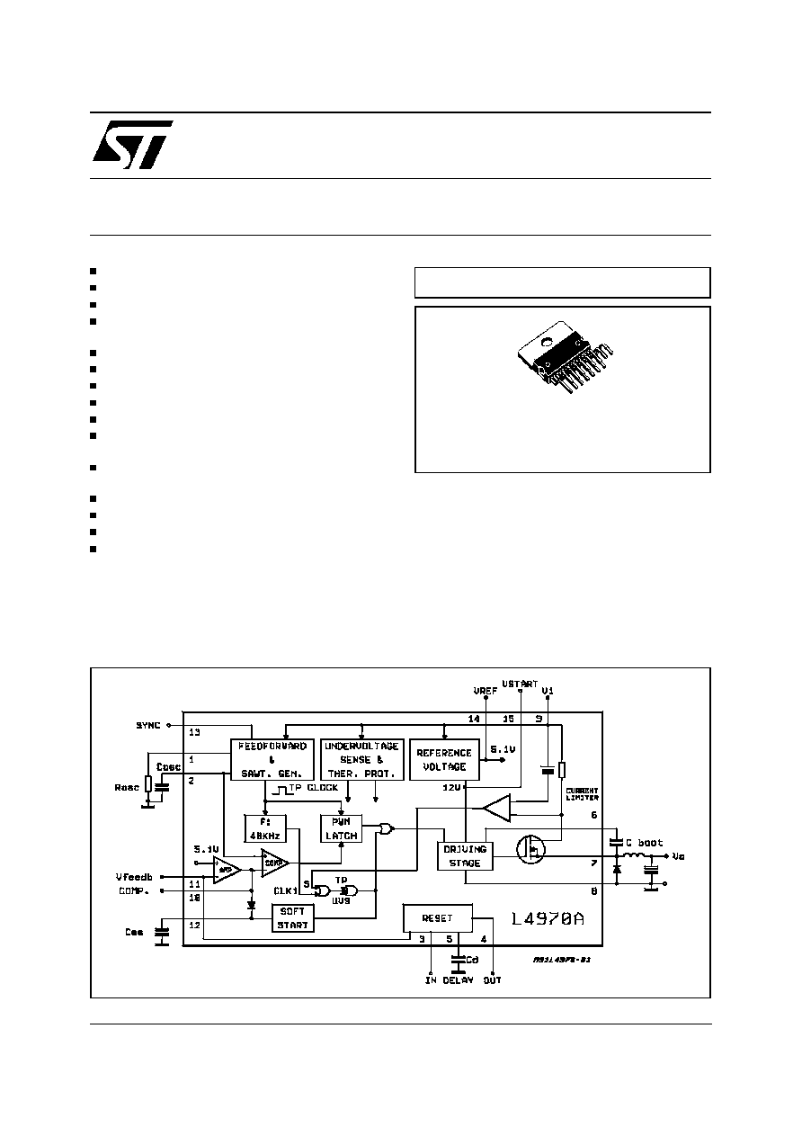
BLOCK DIAGRAM
Multiwatt15V
ORDERING NUMBER: L4970A
MULTIPOWER BCD TECHNOLOGY
1/21
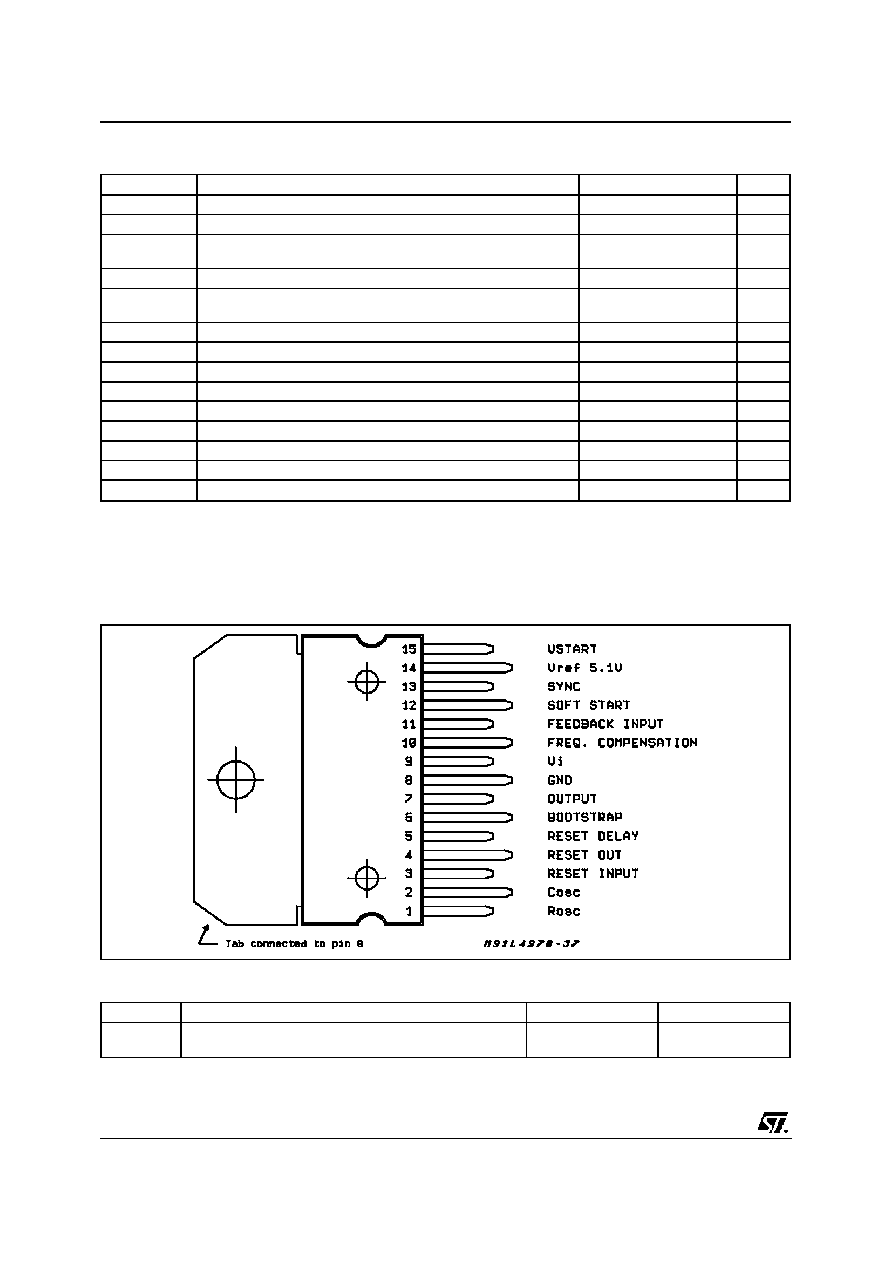
PIN CONNECTION (Top view)
ABSOLUTE MAXIMUM RATINGS
Symbol
Parameter
Value
Unit
V
9
Input Voltage
55
V
V
9
Input Operating Voltage
50
V
V
7
Output DC Voltage
Output Peak Voltage at t = 0.1
µ
s f = 200KHz
-1
-7
V
V
I
7
Maximum Output Current
Internally Limited
V
6
Bootstrap Voltage
Bootstrap Operating Voltage
65
V
9
+ 15
V
V
V
3
, V
12
Input Voltage at Pins 3, 12
12
V
V
4
Reset Output Voltage
50
V
I
4
Reset Output Sink Current
50
mA
V
5
, V
10,
V
11,
V
13
Input Voltage at Pin 5, 10, 11, 13
7
V
I
5
Reset Delay Sink Current
30
mA
I
10
Error Amplifier Output Sink Current
1
A
I
12
Soft Start Sink Current
30
mA
P
tot
Total Power Dissipation at T
case
< 120
∞
C
30
W
T
j
, T
stg
Junction and Storage Temperature
-40 to 150
∞
C
THERMAL DATA
Symbol
Parameter
Value
Unit
R
th j-case
R
th j-amb
Thermal Resistance Junction-case
max
Thermal Resistance Junction-ambient
max
1
35
∞
C/W
∞
C/W
L4970A
2/21

CIRCUIT OPERATION (refer to the block dia-
gram)
The L4970A is a 10A monolithic stepdown switching
regulator working in continuous mode realized in the
new BCD Technology. This technology allows the in-
tegration of isolated vertical DMOS power transistors
plus mixed CMOS/Bipolar transistors.
The device can deliver 10A at an output voltage
adjustable from 5.1V to 40V, and contains diag-
nostic and control functions that make it particu-
larly suitable for microprocessor based systems.
BLOCK DIAGRAM
The block diagram shows the DMOS power tran-
sistor and the PWM control loop. Integrated func-
tions include a reference voltage trimmed to 5.1V
±
2%, soft start, undervoltage lockout, oscillator
with feedforward control, pulse by pulse current
limit, thermal shutdown and finally the reset and
power fail circuit. The reset and power fail circuit
provides an output signal for a microprocessor in-
dicating the status of the system.
Device turn on is around 11V with a typical 1V
hysteresis, this threshold provides a correct volt-
age for the driving stage of the DMOS gate and
the hysteresis prevents instabilities.
An external bootstrap capacitor charged to 12V
by an internal voltage reference is needed to pro-
vide correct gate drive to the power DMOS. The
driving circuit is able to source and sink peak cur-
rents of around 0.5A to the gate of the DMOS
transistor. A typical switching time of the current
in the DMOS transistor is 50ns. Due to the fast
commutation switching frequencies up to 500kHz
are possible.
The PWM control loop consists of a sawtooth os-
cillator, error amplifier, comparator, latch and the
output stage. An error signal is produced by com-
paring the output voltage with the precise 5.1V
±
2% on chip reference. This error signal is then
compared with the sawtooth oscillator, in order to
generate a fixed frequency pulse width modulated
drive for the output stage. A PWM latch is in-
cluded to eliminate multiple pulsing within a pe-
riod even in noisy environments. The gain and
PIN FUNCTIONS
N
o
Name
Function
1
OSCILLATOR
R
osc
. External resistor connected to ground determines the constant charging
current of C
osc
.
2
OSCILLATOR
C
osc
. External capacitor connected to ground determines (with R
osc
) the
switching frequency.
3
RESET INPUT
Input of Power Fail Circuit. The threshold is 5.1V. It may be connected via a
divider to the input for power fail function. It must be connected to the pin 14 an
external 30K
resistor when power fail signal not required.
4
RESET OUT
Open Collector Reset/power Fail Signal Output. This output is high when the
supply and the output voltages are safe.
5
RESET DELAY
A C
d
capacitor connected between this terminal and ground determines the
reset signal delay time.
6
BOOTSTRAP
A C
boot
capacitor connected between this terminal and the output allows to
drive properly the internal D-MOS transistor.
7
OUTPUT
Regulator Output.
8
GROUND
Common Ground Terminal
9
SUPPLY VOLTAGE
Unregulated Input Voltage.
10
FREQUENCY
COMPENSATION
A series RC network connected between this terminal and ground determines
the regulation loop gain characteristics.
11
FEEDBACK INPUT
The Feedback Terminal of the Regulation Loop. The output is connected
directly to this terminal for 5.1V operation; It is connected via a divider for higher
voltages.
12
SOFT START
Soft Start Time Constant. A capacitor is connected between thi sterminal and
ground to define the soft start time constant.
13
SYNC INPUT
Multiple L4970A are synchronized by connecting pin 13 inputs together or via
an external syncr. pulse.
14
V
ref
5.1V V
ref
Device Reference Voltage.
15
V
start
Internal Start-up Circuit to Drive the Power Stage.
L4970A
3/21

Figure 1: Feedforward Waveform
Figure 3: Limiting Current Function
Figure 2: Soft Start Function
L4970A
4/21

stability of the loop can be adjusted by an exter-
nal RC network connected to the output of the er-
ror amplifier. A voltage feedforward control has
been added to the oscillator, this maintains supe-
rior line regulation over a wide input voltage
range. Closing the loop directly gives an output
voltage of 5.1V, higher voltages are obtained by
inserting a voltage divider.
At turn on output overcurrents are prevented by
the soft start function (fig. 2). The error amplifier is
initially clamped by an external capacitor Css and
allowed to rise linearly under the charge of an in-
ternal constant current source.
Output overload protection is provided by a cur-
rent limit circuit (fig. 3). The load current is sensed
by an internal metal resistor connected to a com-
parator. When the load current exceeds a preset
threshold the output of the comparator sets a flip
flop which turns off the power DMOS. The next
clock pulse, from an internal 40kHz oscillator will
reset the flip flop and the power DMOS will again
conduct. This current protection method, ensures
a constant current output when the system is
overloaded or short circuited and limits the
switching frequency, in this condition, to 40kHz.
The Reset and Power fail circuitry (fig 4) gener-
ates an output signal when the supply voltage ex-
ceeds a threshold programmed by an external
voltage divider. The reset signal, is generated
with a delay time programmed by an external ca-
pacitor on the delay pin. When the supply voltage
falls below the threshold or the output voltage
goes below 5V the reset output goes low immedi-
ately. The reset output is an open collector-drain.
Fig 4A shows the case when the supply voltage is
higher than the threshold, but the output voltage
is not yet 5V.
Fig 4B shows the case when the output is 5.1V
but the supply voltage is not yet higher than the
fixed threshold.
The thermal protection disables circuit operation
when the junction temperature reaches about
150
∞
C and has an hysterysis to prevent unstable
conditions.
Figure 4: Reset and Power Fail Functions.
A
B
L4970A
5/21