 | –≠–ª–µ–∫—Ç—Ä–æ–Ω–Ω—ã–π –∫–æ–º–ø–æ–Ω–µ–Ω—Ç: L4974A | –°–∫–∞—á–∞—Ç—å:  PDF PDF  ZIP ZIP |
L4974A
June 2000
3.5A SWITCHING REGULATOR
Æ
.
3.5A OUTPUT CURRENT
.
5.1V TO 40V OUTPUT VOLTAGE RANGE
.
0 TO 90% DUTY CYCLE RANGE
.
INTERNAL FEED-FORWARD LINE REG.
.
INTERNAL CURRENT LIMITING
.
PRECISE 5.1V
±
2% ON CHIP REFERENCE
.
RESET AND POWER FAIL FUNCTIONS
.
INPUT/OUTPUT SYNC PIN
.
UNDER VOLTAGE LOCK OUT WITH HYS-
TERETIC TURN-ON
.
PWM LATCH FOR SINGLE PULSE PER PE-
RIOD
.
VERY HIGH EFFICIENCY
.
SWITCHING FREQUENCY UP TO 200KHz
.
THERMAL SHUTDOWN
.
CONTINUOUS MODE OPERATION
DESCRIPTION
The L4974Ais a stepdownmonolithicpower switch-
ing regulator delivering 3.5A at a voltage variable
from 5.1 to 40V.
Realized with BCD mixed technology, the device
uses a DMOS output transistor to obtain very high
efficiency and very fast switching times. Features of
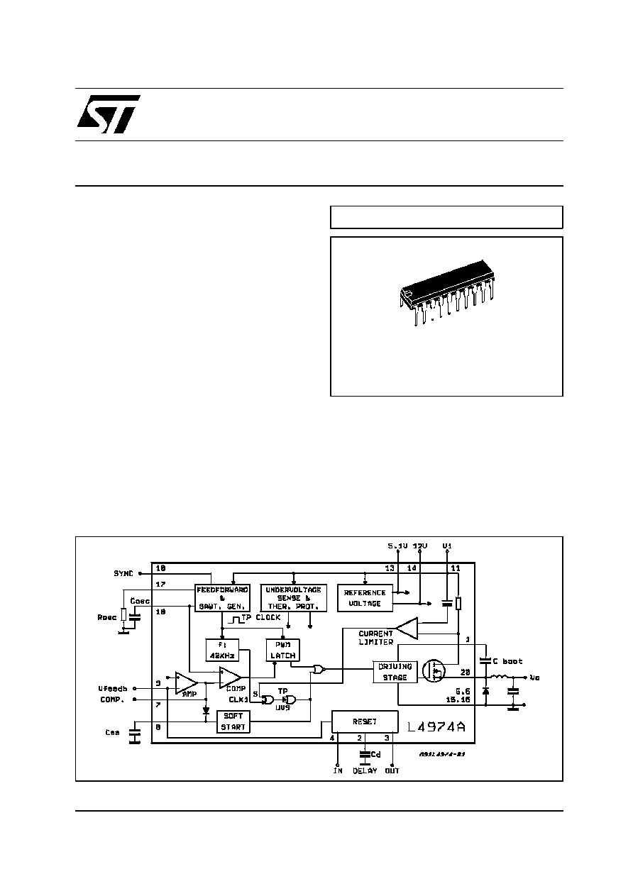
BLOCK DIAGRAM
POWERDI P (16 + 2 + 2)
the L4974A include reset and power fail for micro-
processors, feed forward line regulation, soft start,
limiting current and thermal protection. The device
is mounted in a Powerdip16 + 2 + 2 plastic package
and requires few external components. Efficient
operation at switching frequencies up to 200KHz
allows reductionin the size and cost of external filter
component.
ORDERING NUMBER : L4974A
1/22
This is advanced information on a new product now in development or undergoing evaluation. Details are subject to change without notice.
MULTIPOWER BCD TECHNOLOGY
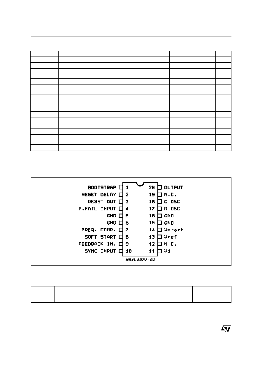
PIN CONNECTION (top view)
THERMAL DATA
Symb ol
Parameter
Valu e
Unit
R
th j-pins
R
th j-amb
Thermal Resistance Junction-Pins
max
Thermal Resistance Junction-ambient
max
12
60
∞
C/W
∞
C/W
ABSOLUTE MAXIMUM RATINGS
Symbo l
Parameter
Valu e
Unit
V
11
Input Voltage
55
V
V
11
Input Operating Voltage
50
V
V
20
Output DC Voltage
Output Peak Voltage at t = 0.1
µ
s f = 200khz
-1
-5
V
V
I
20
Maximum Output Current
Internally Limited
V
I
Boostrap Voltage
Boostrap Operating Voltage
65
V
11
+ 15
V
V
V
4
, V
8
Input Voltage at Pins 4, 12
12
V
V
3
Reset Output Voltage
50
V
I
3
Reset Output Sink Current
50
mA
V
2
, V
7
, V
9
, V
10
Input Voltage at Pin 2, 7, 9, 10
7
V
I
2
Reset Delay Sink Current
30
mA
I
7
Error Amplifier Output Sink Current
1
A
I
8
Soft Start Sink Current
30
mA
P
tot
Total Power Dissipation at T
PINS
90
∞
C
at T
amb
= 70
∞
C (No copper area on PCB)
5
1.3
W
W
T
J
, T
stg
Junction and Storage Temperature
-40 to 150
∞
C
L4974A
2/22
PIN FUNCTIONS
N
o
Name
F unctio n
1
BOOTSTRAP
A C
boot
capacitor connected between this terminal and the output allows to drive
properly the internal D-MOS transistor.
2
RESET DELAY
A C
d
capacitor connected between this terminal and ground determines the reset
signal delay time.
3
RESET OUT
Open Collector Reset/power Fail Signal Output. This output is high when the supply
and the output voltages are safe.
4
RESET INPUT
Input of Power Fail Circuit. The threshold is 5.1V. It may be connected via a divider
to the input for power fail function. It must be connected to the pin 14 an external 30K
resistor when power fail signal not required.
5, 6
15, 16
GROUND
Common Ground Terminal
7
FREQUENCY
COMPENSATION
A series RC network connected between this terminal and ground determines the
regulation loop gain characteristics.
8
SOFT START
Soft Start Time Constant. A capacitor is connected between thi sterminal and ground
to define the soft start time constant.
9
FEEDBACK INPUT
The Feedback Terminal of the Regulation Loop. The output is connected directly to
this terminal for 5.1V operation; It is connected via a divider for higher voltages.
10
SYNC INPUT
Multiple L4974A's are synchronized by connecting pin 10 inputs together or via an
external syncr. pulse.
11
SUPPLY VOLTAGE
Unregulated Input Voltage.
12, 19
N.C.
Not Connected.
13
V
ref
5.1V V
ref
Device Reference Voltage.
14
V
start
Internal Start-up Circuit to Drive the Power Stage.
17
OSCILLATOR
R
osc
. External resistor connected to ground determines the constant charging current
of C
osc
.
18
OSCILLATOR
C
osc
. External capacitor connected to ground determines (with R
osc
) the switching
frequency.
20
OUTPUT
Regulator Output.
L4974A
3/22

The L4974A is a 3.5A monolithic stepdown switch-
ing regulatorworking in continuousmode realized in
the new BCD Technology. This technology allows
theintegrationof isolatedvertical DMOS powertran-
sistors plus mixed CMOS/Bipolar transistors.
The device can deliver 3.5A at an outputvoltagead-
justable from 5.1V to 40V and contains diagnostic
and control functions that make it particularly suit-
able for microprocessor based systems.
BLOCK DIAGRAM
The block diagram shows the DMOS power tran-
sistors and the PWM control loop. Integrated func-
tions include a reference voltage trimmed to 5.1V
±
2%, soft start, undervoltagelockout, oscillator with
feedforward control, pulse by pulse current limit,
thermal shutdown and finally the reset and power
fail circuit. The reset and power fail circuit provides
an output signal for a microprocessor indicating the
status of the system.
Device turn on is around 11V with a typical 1V hys-
terysis, this threshold porvides a correct voltage for
the driving stage of the DMOS gate and the hyste-
rysis prevents instabilities.
An externalbootstrapcapacitor chargeto 12V by an
internal voltage reference is needed to provide cor-
rect gate drive to the power DMOS. The driving cir-
cuit is able to source and sink peak currents of
around 0.5A to the gate of the DMOS transistor. A
typical switching time of the current in the DMOS
transistor is 50ns. Due to the fast commutation
switching frequencies up to 200kHz are possible.
The PWM control loop consists of a sawtooth oscil-
lator, error amplifier, comparator, latch and the out-
put stage. An error signal is producedby comparing
theoutputvoltagewiththe precise5.1V
±
2% on chip
reference. This error signal is then compared with
the sawtooth oscillator in order to generate frixed
frequency pulse width modulated drive for the out-
put stage. A PWM latch is included to eliminate
multiple pulsing within a period even in noisy envi-
ronments.
The gain and stability of the loop can be adjustedby
an external RC network connected to the output of
the error amplifier. A voltage feedforward control
has been added to the oscillator, this maintains su-
perior line regulation over a wide input voltage
range. Closing the loop directly gives an output vol-
tage of 5.1V, higher voltages areobtained by insert-
ing a voltage divider.
At turn on, outputovercurrents are prevented by the
soft start function (fig. 2). The error amplifier is in-
itially clamped by an externalcapacitor,Css, and al-
lowed to rise linearly under the charge of an internal
constant current source.
Output overload protection is provided by a current
limit circuit. The load current is sensed by a internal
metalresistor connectedto a comparator.When the
load current exceeds a preset threshold, the output
of the comparator sets a flip flop which turns off the
power DMOS. The next clock pulse, from an internal
40kHz oscillator, will reset the flip flop and the power
DMOS will again conduct. This current protection
method,ensuresa constantcurrent outputwhen the
systemis overloadedor shortcircuited and limitsthe
switching frequency, in this condition,to 40kHz. The
Reset and Power fail circuit (fig. 4), generates an
output signal when the supply voltage exceeds a
threshold programmed by an external voltage di-
vider. The reset signal, is generated with a delay
time programmed by a externalcapacitor on the de-
lay pin. When the supply voltage falls below the
threshold or the output voltage goes below 5V, the
reset output goes low immediately. The reset output
is an open drain.
Fig. 4A shows the case when the supply voltage is
higher than the threshold, but the output voltage is
not yet 5V.
Fig. 4B shows the case when the output is 5.1V, but
the supply voltage is not yet higher than the fixed
threshold.
The thermal protection disables circuit operation
when the junction temperature reaches about
150
∞
C and has a hysterysis to prevent unstable
conditions.
CIRCUIT OPERATION
L4974A
4/22
Figure 1 : Feedforward Waveform.
Figure 2 : Soft Start Function.
Figure 3 : Limiting Current Function.
L4974A
5/22

Figure 4 : Reset and Power Fail Functions.
B
A
L4974A
6/22

ELECTRICAL CHARACTERISTICS (refer to the test circuit, T
J
= 25
∞
C, V
i
= 35V, R
4
= 30K
,
C
9
= 2.7nF, f
SW
= 100KHz typ, unless otherwise specified)
DYNAMIC CHARACTERISTICS
Symbo l
Parameter
T est Co nd iti ons
Mi n.
T yp.
Max.
Unit
Fig .
V
i
Input Volt. Range (pin 11)
V
o
= V
ref
to 40V
I
o
= 3.5A (*)
15
50
V
5
V
o
Output Voltage
V
i
=15V to 50V
I
o
= 2A; V
o
= V
ref
5
5.1
5.2
V
5
V
o
Line Regulation
V
I
= 15V to 50V
I
o
= 1A; V
o
= V
ref
12
30
mV
V
o
Load Regulation
V
O
= V
ref
I
o
= 1A to 3.5A
I
o
= 2A to 3A
8
25
mV
4
10
mV
V
d
Dropout Voltage between
Pin 11 and 20
I
o
= 2A
I
o
= 3.5A
0.25
0.45
0.4
0.7
V
I
20L
Max Limiting Current
V
i
= 15V to 50V
V
o
= V
ref
to 40V
4
4.75
5.5
A
Efficiency
I
o
= 3.5A, f = 100KHz
V
o
= V
ref
V
o
= 12V
80
85
90
%
%
SVR
Supply Voltage Ripple
Rejection
V
i
= 2VRMS; I
o
= 5A
f = 100Hz; V
o
= V
ref
56
60
dB
5
f
Switching Frequency
90
100
110
KHz
5
f/
Vi
Voltage
Stability
of
Switching
Frequency
V
i
= 15V to 45V
2
6
%
5
f/T
j
Temperature Stability of
Switching Frequency
T
j
= 0 to 125
∞
C
1
%
5
f
max
Maximum Operating
Switching Frequency
V
o
= V
ref
R
4
= 15K
I
o
= 3.5A C
9
= 2.2nF
200
KHz
5
(*) Pulse testing with a low duty cycle
V
ref
SECTION (pin 13)
Symbo l
Parameter
T est Cond iti on
Mi n.
T yp.
Max.
Unit
Fig .
V
13
Reference Voltage
5
5.1
5.2
V
7
V
13
Line Regulation
V
i
= 15V to 50V
10
25
mV
7
V
13
Load Regulation
I
13
= 0 to 1mA
20
40
mV
7
V
13
T
Average
Temperature
Coefficient
Reference
Voltage
T
j
= 0
∞
C to 125
∞
C
0.4
mV/
∞
C
7
I
13 short
Short Circuit Current Limit
V
13
= 0
70
mA
7
V
START
SECTION (pin 15)
Symbo l
Parameter
T est Cond iti on
Mi n.
T yp.
Max.
Unit
Fig .
V
14
Reference Voltage
11.4
12
12.6
V
7
V
14
Line Regulation
V
i
= 15 to 50V
0.6
1.4
V
7
V
14
Load Regulation
I
14
= 0 to 1mA
50
200
mV
7
I
14 short
Short Circuit Current Limit
V
15
= 0V
80
mA
7
L4974A
7/22
ELECTRICAL CHARACTERISTICS (continued)
DC CHARACTERISTICS
Symbo l
Parameter
T est Cond iti on
Mi n.
Typ.
Max.
Unit
F ig.
V
11on
Turn-on Threshold
10
11
12
V
7A
V
11 Hyst
Turn-off Hysteresys
1
V
7A
I
11Q
Quiescent Current
V
8
= 0; S1 = D
13
19
mA
7A
I
11OQ
Operating Supply Current
V
8
= 0; S1 = B; S2 = B
16
23
mA
7A
I
20L
Out Leak Current
V
i
= 55V; S3 = A; V
8
= 0
2
mA
7A
SOFT START (pin 8)
Symbo l
Parameter
T est Cond iti on
Mi n.
Typ.
Max.
Unit
F ig.
I
8
Soft Start Source Current
V
8
= 3V; V
9
= 0V
80
115
150
µ
A
7B
V
8
Output Saturation Voltage
I
8
= 20mA; V
11
= 10V
I
8
= 200
µ
A; V
11
= 10V
1
0.7
V
V
7B
7B
ERROR AMPLIFIER
Symbo l
Parameter
T est Cond iti on
Mi n.
Typ.
Max.
Unit
F ig.
V
7H
High Level Out Voltage
I
7
= -100
µ
A; S1 = C
V
9
= 4.7V
6
V
7C
V
7L
Low Level Out Voltage
I
7
= 100
µ
A; S1 = C
V
9
= 5.3V;
1.2
V
7C
I
7H
Source Output Current
V
7
= 1V; V
7
= 4.7V
100
150
µ
A
7C
-I
7L
Sink Output Current
V
7
= 6V; V
9
= 5.3V
100
150
µ
A
7C
I
9
Input Bias Current
S1 = B; R
S
= 10K
0.4
3
µ
A
7C
G
V
DC Open Loop Gain
S1 = A; R
S
= 10
60
dB
7C
SVR
Supply Voltage Rejection
15 < V
i
< 50V
60
80
dB
7C
V
OS
Input Offset Voltage
R
S
= 50
S1 = A
2
10
mV
7C
RAMP GENERATOR (pin 18)
Symbo l
Parameter
T est Cond iti on
Mi n.
Typ.
Max.
Unit
F ig.
V
18
Ramp Valley
S1 = B; S2 = B
1.2
1.5
V
7A
V
18
Ramp Peak
S1 = B
V
i
= 15V
S2 = B
V
i
= 45V
2.5
5.5
V
V
7A
7A
I
18
Min. Ramp Current
S1 = A; I
17
= 100
µ
A
270
300
µ
A
7A
I
18
Max. Ramp Current
S1 = A; I
17
= 1mA
2.4
2.7
mA
7A
SYNC FUNCTION (pin 10)
Symbo l
Parameter
T est Cond iti on
Mi n.
Typ.
Max.
Unit
F ig.
V
10
Low Input Voltage
V
i
= 15V to 50V; V
8
= 0;
S1 = B; S2 = B; S4 = B
≠0.3
0.9
V
7A
V
10
High Input voltage
V
8
= 0;
S1 = B; S2 = B; S4 = B
2.5
5.5
V
7A
+I
10L
Sync Input Current with Low
Input Voltage
V
10
= V
18
= 0.9V; S4 = B;
S1 = B; S2 = B
0.4
mA
7A
+I
10H
Input Current with
High
Input Voltage
V
10
= 2.5V
1.5
mA
7A
V
10
Output Amplitude
4
5
V
≠
t
W
Output Pulse Width
V
thr
= 2.5V
0.3
0.5
0.8
µ
s
≠
L4974A
8/22
RESET AND POWER FAIL FUNCTIONS
Symbo l
Parameter
T est Co nd iti ons
Mi n.
T yp.
Max.
Unit
Fig .
V
9R
Rising Thereshold Voltage
(pin 9)
V
i
= 15 to 50V
V
4
= 5.3V
V
ref
-130
V
ref
-100
V
ref
-80
V
mV
7D
V
9F
Falling Thereshold Voltage
(pin 9)
Vi = 15 to 50V
V
4
= 5.3V
4.77
Vref
-200
V
ref
-160
V
mV
7D
V
2H
Delay High Threshold Volt.
Vi = 15 to 50V
V
4
= 5.3V V
9
= V
13
4.95
5.1
5.25
V
7D
V
2L
Delay Low Threshold Volt.
Vi = 15 to 50V
V
4
= 4.7V
V
9
= V
13
1
1.1
1.2
V
7D
I
2SO
Delay Source Current
V
4
= 5.3V;
V
2
= 3V
30
60
80
µ
A
7D
I
2SI
Delay Source Sink Current
V
4
= 4.7V; V
2
= 3V
10
mA
7D
V
3S
Output Saturation Voltage
I
3
= 15mA; S1 = B V
4
= 4.7V
0.4
V
7D
I
3
Output Leak Current
V3 = 50V; S1 = A
100
µ
A
7D
V
4R
Rising Threshold Voltage
V9 = V
13
4.955
5.1
5.25
V
7D
V
4H
Hysteresis
0.4
0.5
0.6
V
7D
I
4
Input Bias Current
1
3
µ
A
7D
ELECTRICAL CHARACTERISTICS (continued)
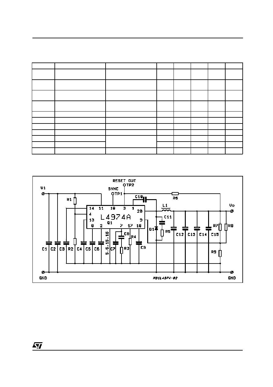
Figure 5 : Test and Evaluation Board Circuit.
TYPICAL PERFORMANCES (using evaluation board) :
n = 83% (V
i
= 35V ; V
o
= VREF ; I
o
= 3.5A ; f
sw
= 100KHz)
V
o RIPPLE
= 30mV (at 1A)
Line regulation = 12mV (V
i
= 15 to 50V)
Load regulation = 8mV (I
o
= 1 to 3.5A)
for component values Refer to the fig. 5 (Part list).
L4974A
9/22
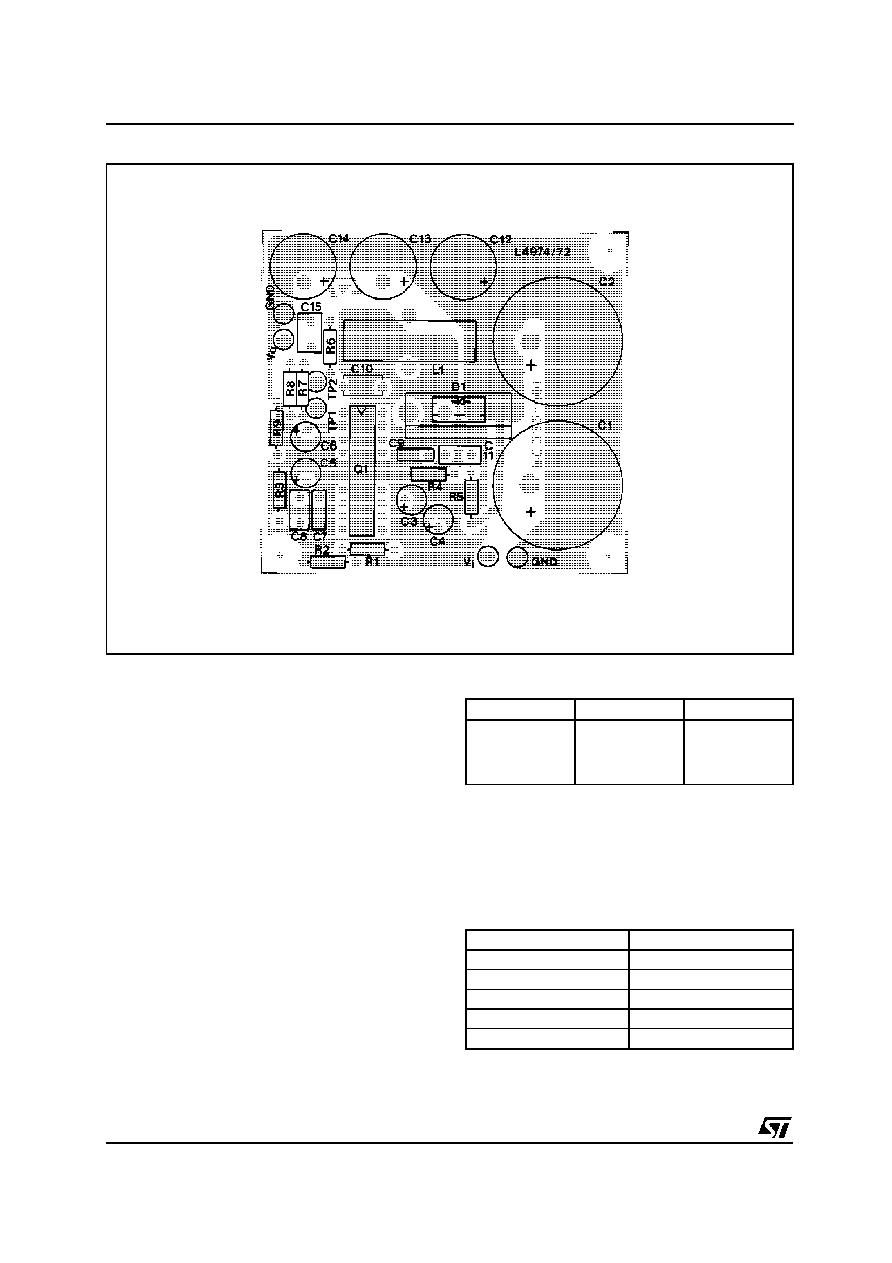
PART LIST
R
1
= 30K
R
2
= 10K
R
3
= 15K
R
4
= 30K
R
5
= 22
R
6
= 4.7K
R
7
= see table A
R
8
= OPTION
R
9
= 4.7K
* C
1
= C
2
= 1000
µ
F 63V EYF (ROE)
C
3
= C
4
= C
5
= C
6
= 2,2
µ
F 50V
C
7
= 390pF Film
C
8
= 22nF MKT 1837 (ERO)
C
9
= 2.7nF KP 1830 (ERO)
C
10
= 0.33
µ
F Film
C
11
= 1nF
** C
12
= C
13
= C
14
= 100
µ
F 40V EKR (ROE)
C
15
= 1
µ
F Film
D1 = SB 560 (OR EQUIVALENT)
L1 = 150
µ
H
core 58310 MAGNETICS
45 TURNS 0.91mm (AWG 19)
COGEMA 949181
* 2 capacitors in parallel to increase input RMS current capability.
* * 3 capacitors in parallel to reduce total output ESR.
Table A
V
0
R
9
R
7
12V
15V
18V
24V
4.7k
4.7k
4.7k
4.7k
6.2kW
9.1k
12
18
Table B
SUGGESTED BOOSTRAP CAPACITORS
Operatin g F requency
Boo strap Cap.c10
f = 20KHz
680nF
f = 50KHz
470nF
f = 100KHz
330nF
f = 200KHz
220nF
f = 500KHz
100nF
Figure 6a : Component Layout of fig.5 (1 : 1 scale). Evaluation Board Available
L4974A
10/22
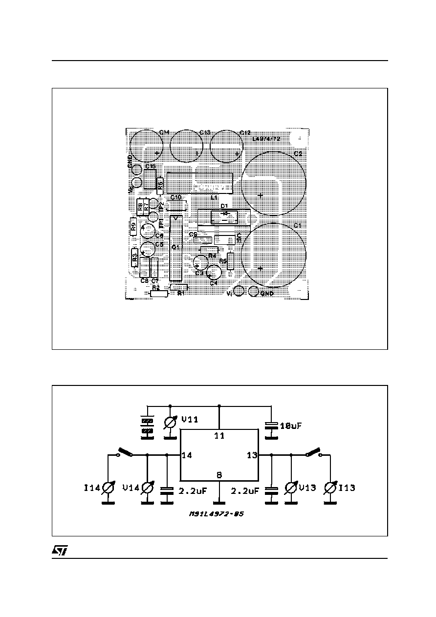
Figure 7 : DC Test Circuits.
Figure 6b: P.C. Board and Component Layout of the Circuit of Fig. 5. (1:1 scale)
L4974A
11/22

Figure 7C.
Figure 7B.
Figure 7A.
L4974A
12/22
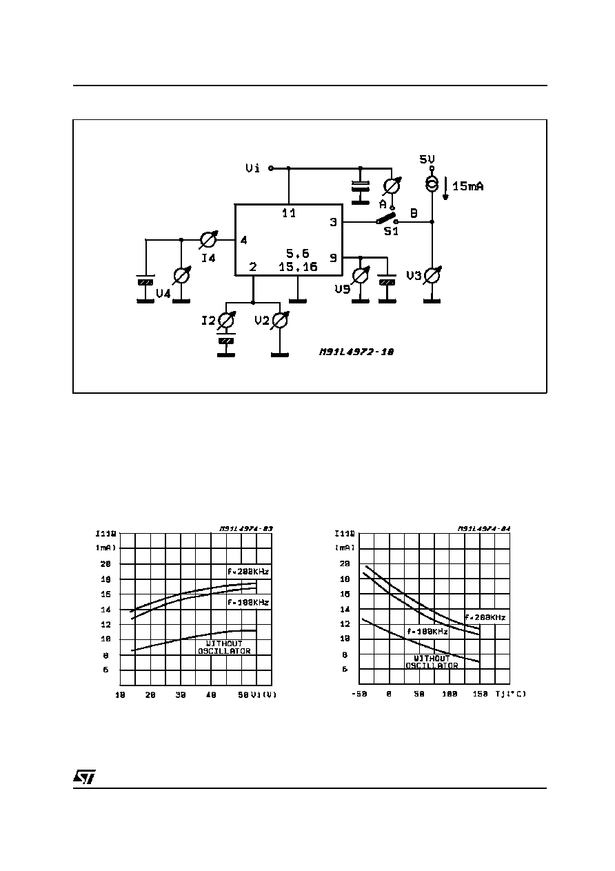
Figure 7D.
Figure 8 : Quiescent Drain Current vs. Supply
Voltage (0% duty cycle - see fig. 7A).
Figure 9 : Quiescent Drain Current vs. Junction
Temperature (0% duty cycle).
L4974A
13/22
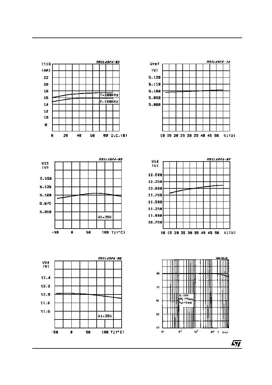
Figure 10 : Quiescent Drain Current vs. Duty Cy-
cle.
Figure 11 : Reference Voltage (pin 13) vs. Vi
(see fig. 7).
Figure 12 : Reference Voltage (pin 13) vs. Junc-
tion Temperature (see fig. 7).
Figure 13 : ReferenceVoltage (pin 14) vs. Vi
(see fig. 7).
Figure 14 : Reference Voltage (pin 14) vs. Junc-
tion Temperature (see fig. 7).
Figure 15 : Reference Voltage 5.1V (pin 13) Sup-
ply Voltage Ripple Rejection vs. Fre-
SVR
(dB)
L4974A
14/22
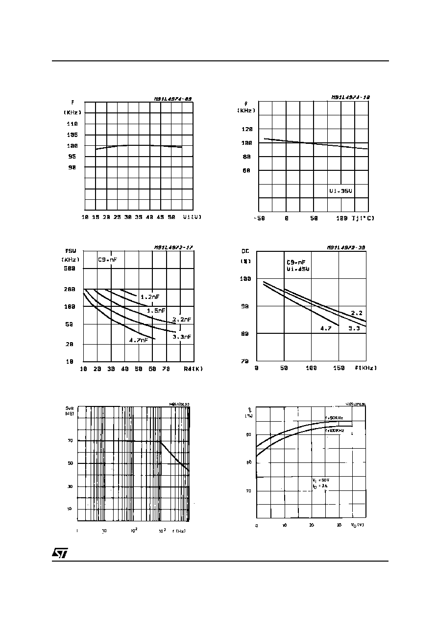
Figure 16 : Switching Frequency vs. Input Voltage
(see fig. 5).
Figure 17 : Switching Frequency vs. Junction
Temperature (see fig. 5).
Figure 18 : Switching Frequency vs. R4
(see fig.5).
Figure 19 : Maximum Duty Cycle vs. Frequency.
Figure 20 : Supply Voltage Ripple Rejection vs.
Frequency (see fig. 5).
Figure 21 : Efficiency vs. Output Voltage.
L4974A
15/22
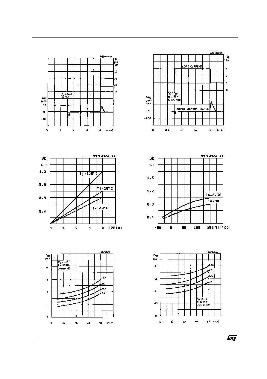
Figure 22 : Line Transient Response (see fig. 5).
Figure 23 : Load Transient Response (see fig. 5).
Figure 24 : Dropout Voltage between Pin 11 and
Pin 20 vs. Current at Pin 20.
Figure 25 : .Dropout Voltage between Pin 11 and
Pin 20 vs. Junction Temperature.
Figure 26 : Power Dissipation (device only) vs.
Input Voltage.
Figure 27 : Power Dissipation (device only) vs.
Input Voltage.
L4974A
16/22

Figure 28 : Power Dissipation (device only) vs.
Output Voltage.
Figure 29 : Power Dissipation (device only) vs.
Output Voltage.
Figure 30 : Power Dissipation (device only) vs.
Output Current.
Figure 31 : Power Dissipation (device only) vs.
Output Current.
Figure 32 : Efficiency vs. Output Current.
Figure 33 : Test PCB Thermal Characteristic.
L4974A
17/22

Figure 34 : Junction to AmbientThermal Resistance
vs. Area onBoard Heatsink (DIP 16+2+2)
Figure 35: Maximum Allowable Power Dissipa-
tion vs. Ambient Temperature (Pow-
erdip)
Figure 36: Open Loop Frequency and Phase of Er-
ror Amplifier (see fig. 7C).
L4974A
18/22

Figure 37 : 3.5A ≠ 5.1V Low Cost Application Circuit.
Figure 38 : A 5.1V/12V Multiple Supply. Note the Synchronization between the L4974A and L4970A.
L4974A
19/22

Figure 39 : L4974A's Sync. Example.
Figure 40: 1A/24V Multiple Supply. Note the synchronization between the L4974A and L4962
L4974A
20/22

DIM.
mm
inch
MIN.
TYP.
MAX.
MIN.
TYP.
MAX.
a1
0.51
0.020
B
0.85
1.40
0.033
0.055
b
0.50
0.020
b1
0.38
0.50
0.015
0.020
D
24.80
0.976
E
8.80
0.346
e
2.54
0.100
e3
22.86
0.900
F
7.10
0.280
I
5.10
0.201
L
3.30
0.130
Z
1.27
0.050
Powerdip 20
OUTLINE AND
MECHANICAL DATA
L4974A
21/22

Information furnished is believed to be accurate and reliable. However, STMicroelectronics assumes no responsibility for the conse-
quences of use of such information nor for any infringement of patents or other rights of third parties which may result from its use. No
license is granted by implication or otherwise under any patent or patent rights of STMicroelectronics. Specification mentioned in this
publication are subject to change without notice. This publication supersedes and replaces all information previously supplied. STMi-
croelectronics products are not authorized for use as critical components in life support devices or systems without express written
approval of STMicroelectronics.
The ST logo is a registered trademark of STMicroelectronics
©
2000 STMicroelectronics ≠ Printed in Italy ≠ All Rights Reserved
STMicroelectronics GROUP OF COMPANIES
Australia - Brazil - China - Finland - France - Germany - Hong Kong - India - Italy - Japan - Malaysia - Malta - Morocco -
Singapore - Spain - Sweden - Switzerland - United Kingdom - U.S.A.
http://www.st.com
L4974A
22/22