1/10
L4979D
L4979MD
October 2004
1
FEATURES
OPERATING DC SUPPLY VOLTAGE RANGE
5.6V TO 31V
LOW QUIESCENT CURRENT
(6
Ķ
A Typ. @ 25įC with Enable Low)
HIGH PRECISION OUTPUT VOLTAGE (2%)
LOW DROPOUT VOLTAGE LESS THAN 0.5V
RESET CIRCUIT SENSING THE OUTPUT
VOLTAGE DOWN TO 1V
PROGRAMMABLE RESET PULSE DELAY
WITH EXTERNAL CAPACITOR
WATCHDOG
PROGRAMMABLE WATCHDOG TIMER WITH
EXTERNAL CAPACITOR
THERMAL SHUTDOWN AND SHORT
CIRCUIT PROTECTION
AUTOMOTIVE TEMPERATURE RANGE
(Tj = -40įC TO 150įC)
ENABLE INPUT FOR ENABLING/DISABLING
THE VOLTAGE REGULATOR OUTPUT
LOW DROP VOLTAGE REGULATOR
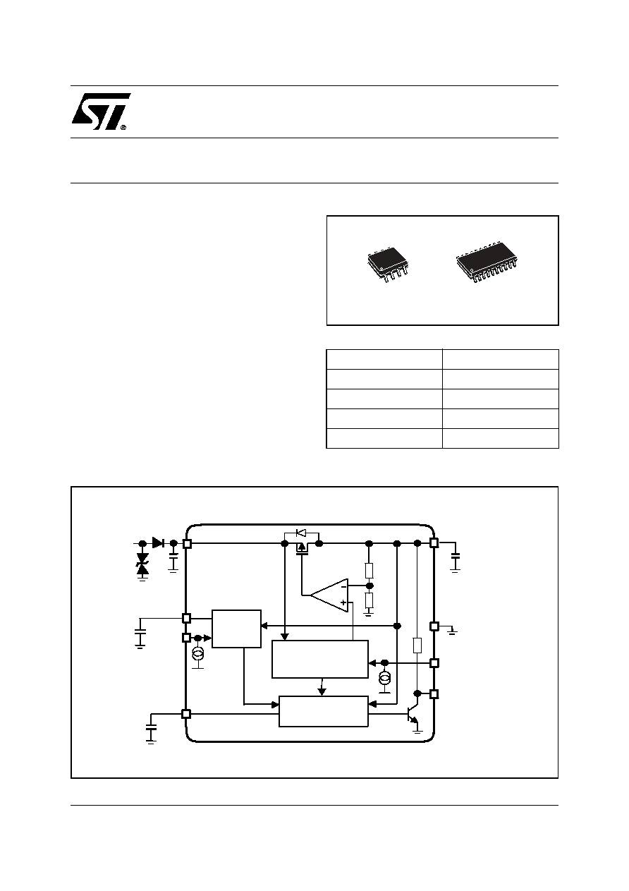
Figure 2. Block Diagram
Voltage reference
reset
watchdog
Vs
Vi
Wi
Vcw
Vcr
Ctr
Ctw
Res
En
gnd
Vo
Co
5V, 150 mA
Voltage reference
reset
watchdog
Vs
Vi
Wi
Vcw
Vcr
Ctr
Ctw
Res
En
gnd
Vo
Co
5V, 150 mA
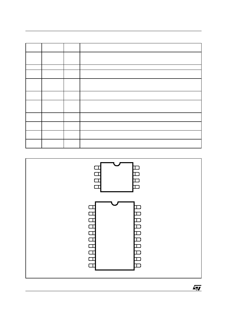
Figure 1. Packages
Table 1. Order Codes
Part Number
Package
L4979D
SO-8
L4979MD
SO-20
L4979D13TR
SO-8 Tape & Reel
L4979MD13TR
SO-20 Tape & Reel
SO-8
SO-20
Rev. 5
L4979MD L4979D
2/10
Table 2. Pin Function
Figure 3. Pins Connection (Top view)
SO8
Nį
SO20
Nį
Pin
Name
Function
1
1
En
Enable input
If high, regulator, watchdog and reset are operating. If low, regulator, watchdog
and reset are shut down.
2
4
gnd
Ground reference
5,6,15,16
gnd
Ground
These pins are to be connected to a heat spreader electrically grounded
3
7
Res
Reset output.
It is pulled down when output voltage drops below Vo_th or frequency at Wi is too
low.
4
10
Vcr
Reset timing adjust
A capacitor between Vcr pin and gnd sets the reset delay time (trd)
5
11
Vcw
Watchdog timer adjust
A capacitor between Vcw pin and gnd sets the time response of the watchdog
monitor.
6
14
Wi
Watchdog input.
If the frequency at this input pin is too low, the Reset output is activated.
7
17
Vo
Voltage regulator output
Output capacitor >100nF is needed for regulator stability
8
20
Vs
Supply voltage
Supply capacitor (e.g. 200nF) is needed for regulator stability.
2, 3, 8, 9, 12,
13, 18, 19
N. C.
not connected
EN
GND
RES
VCR
VCW
WI
V
O
V
S
1
3
2
4
6
5
7
8
SO8
EN
N.C.
N.C.
GND
GND
RES
GND
N.C.
N.C.
N.C.
N.C.
WI
GND
GND
V
O
N.C.
N.C.
V
S
1
3
2
4
5
6
7
8
9
18
17
16
15
14
12
13
11
19
10
20
VCR
WCW
D00AT457
SO8
SO20
3/10
L4979MD L4979D
Table 3. Absolute Maximum Ratings
Note:
1. Maximum ratings are absolute ratings; exceeding any one of these values may cause permanent damage to the integrated circuit.
Table 4. Thermal DatA
Table 5. Electrical Characteristcs
(V
s
= 5.6V to 31V, T
j
= -40įC to +150įC unless otherwise specified)
Symbol
Parameter
Value
Unit
Vvsdc
DC supply voltage
-0.3 to 40
V
Ivsdc
Input current
internally limited
Vvo
DC output voltage
-0.3 to 6
V
Ivo
DC output current
internally limited
Vwi
Watchdog input voltage
-0.3 to V
vo
+0.3
V
Vod
Open drain output voltage (RES)
-0.3 to V
vo
+0.3
V
Iod
Open drain output current (RES)
internally limited
Vcr
Reset delay voltage
-0.3 to V
vo
+0.3
V
Vcw
Watchdog delay voltage
-0.3 to V
vo
+0.3
V
Ven
Enable input voltage
-0.3 to 40
V
Tj
Junction temperature
-40 to 150
įC
VESD
ESD voltage level (HBM-MIL STD 883C)
Ī2
kV
Symbol
Parameter
SO8
SO16+2+2
Unit
R
th j-amb
Thermal resistance Junction to Ambient
130 to 180
50 to 80
įC/W
Pin
Symbol
Parameter
Test Condition
Min.
Typ.
Max.
Unit
GENERAL
V
s
, V
o
I
q
Quiescent current
V
s
= 13.5V, I
o
=150mA,
enable high
all I/O currents=0
1.5
3
mA
V
s
, V
o
I
q
Quiescent current
V
s
= 13.5V, I
o
= 0mA,
enable high
all I/O currents = 0
100
200
Ķ
A
V
s
, V
o
I
q
Quiescent current
V
s
= 13.5V, I
o
= 0mA,
enable low
all I/O currents = 0
6
20
Ķ
A
T
w
Thermal protection
temperature
150
190
įC
T
w_hy
Thermal protection
temperature hysteresis
10
įC
L4979MD L4979D
4/10
VOLTAGE REGULATOR
V
o
V
o_ref
Output voltage
V
s
= 5.6 to 31V
I
o
= 1 to 150mA
4.90
5.00
5.10
V
V
o
I
short
Output short circuit current
(1)
V
s
= 13.5V
150
280
400
mA
V
o
I
lim
Output current limitation
(1)
V
s
= 13.5V
150
320
500
mA
V
s
, V
o
V
line
Line regulation voltage
V
s
= 5.6 to 31V
I
o
= 1 to 150mA
25
mV
V
o
V
load
Load regulation voltage
I
o
= 1 to 150mA
25
mV
V
s
, V
o
V
dp
Drop voltage
I
o
= 150mA
200
400
mV
V
s
, V
o
SVR
Ripple rejection
(2)
f
r
= 100 Hz
55
dB
RESET
R
es
V
res_l
Reset output low voltage
R
ext
= 5k
to Vo,
Vo > 1V
0.4
V
R
es
I
res_h
Reset output high leakage
current
V
res
= 5V
1
Ķ
A
R
es
R
_p_u
Internal Pull up resistance
with respect to V
o
12
25
50
k
R
es
V
o_th
Reset threshold voltage
V
s
= 5.6 to 31V
I
o
= 1 to 150mA
6%
below
V
o_ref
8%
below
V
o_ref
10%
below
V
o_ref
V
cr
V
rhth
Reset timing high threshold
V
s
= 13.5V
44%
V
o_ref
47%
V
o_ref
50%
V
o_ref
V
cr
V
rlth
Reset timing low threshold
V
s
= 13.5V
10%
V
o_ref
13%
V
o_ref
16%
V
o_ref
V
cr
I
cr
Charge current
V
s
= 13.5V
8
17
30
Ķ
A
V
cr
I
dr
Discharge current
V
s
= 13.5V
8
17
30
Ķ
A
R
es
t
rr_2
Reset delay time (3)
Vo = V
o_th
-100mV
100
250
700
Ķ
s
R
es
t
rd
Reset pulse delay
V
s
= 13.5V, C
tr
= 1nF
65
150
ms
WATCHDOG
W
i
V
ih
Input high voltage
V
s
= 13.5V
3.5
V
W
i
V
il
Input low voltage
V
s
= 13.5V
1.5
V
W
i
V
ih
Input hysteresis
V
s
= 13.5V
300
mV
W
i
I
i
Pull down current
V
s
= 13.5V
10
20
Ķ
A
V
cw
V
whth
High threshold
V
s
= 13.5V
2.20
2.35
2.50
V
V
cw
V
wlth
Low threshold
V
s
= 13.5V
0.50
0.65
0.80
V
Pin
Symbol
Parameter
Test Condition
Min.
Typ.
Max.
Unit
Table 5: Electrical Characteristics (continued)
5/10
L4979MD L4979D
Note:
1. see fig4 (behavior of output current versus regulated voltage Vo)
2. guaranteed by design
3. When Vo becomes lower than 4V, the reset reaction time decreases down to 2
Ķ
s assuring a faster reset condition in this particular
case.
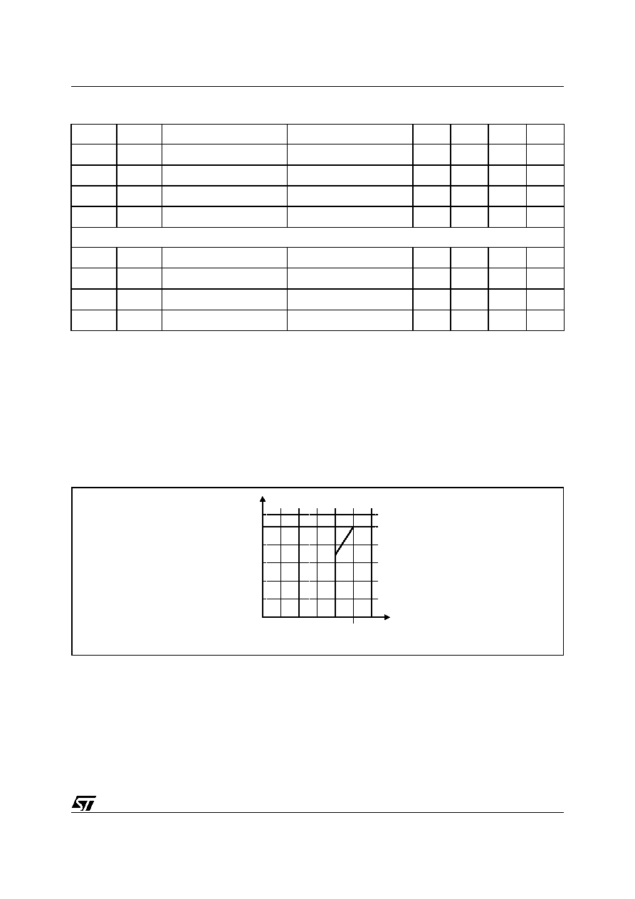
2
VOLTAGE REGULATOR
The voltage regulator uses a p-channel MOS transistor as a regulating element. With this structure a low drop-
out voltage at current up to 150mA is achieved. The output voltage is regulated up to transient input supply volt-
age of 40V. No functional interruption due to over-voltage pulses is generated. The high precision of the output
voltage is obtained with a pre-trimmed reference voltage. A short circuit protection to GND is provided.
Figure 4. Behavior of output current versus regulated voltage Vo (see a.m. Note 1)
3
RESET
The reset circuit monitors the output voltage Vo. If the output voltage drops below V
o_th
then Res becomes low
with a delay time trr. Real trr value changes as a non-linear function of delta (V
o-th
- V
o
). The reset low signal is
guaranteed for an output voltage Vo greater than 1V.
When the output voltage becomes higher than Vo_th then Res goes high with a delay trd. This delay is obtained
by 512 periods of an oscillator (see fig. 5). The oscillator period is given by:
V
cw
I
cwc
Charge current
V
s
= 13.5V, V
cw
= 0.1V
4
7.5
14
Ķ
A
V
cw
I
cwd
Discharge current
V
s
= 13.5V, V
cw
= 2.5V
1.0
2.4
4.5
Ķ
A
V
cw
T
wop
Watchdog period
V
s
= 13.5V, C
tw
= 47nF
25
50
90
ms
R
es
t
wol
Watchdog output low time
V
s
= 13.5V, C
tw
= 47nF
6
10
22
ms
ENABLE
E
n
V
en_l
Enable input low voltage
1
V
E
n
V
en_h
Enable input high voltage
3
V
E
n
V
en_hy
Enable input hysteresis
700
1000
1100
mV
E
n
I
_leak
Pull down current
E
n
= 5V
2
10
20
Ķ
A
Pin
Symbol
Parameter
Test Condition
Min.
Typ.
Max.
Unit
Vo
Vo_ref
Iout
Ishort Ilim
Vo
Vo_ref
Iout
Ishort Ilim
ELECTRICAL CHARACTERISTICS (continued)

L4979MD L4979D
6/10
and reset pulse delay trd is given by:
t
rd
= 512 x T
osc
Figure 5. Reset Time Diagram.
4
WATCHDOG
The watchdog input Wi monitors a connected microcontroller. If pulses are missing, the reset output Res is
set to low. The pulse sequence time can be set within a wide range thorough the external capacitor C
tw
. The
watchdog circuit discharges the capacitor C
tw
with the constant current Icwd. If the lower threshold Vwlth is
reached, a watchdog reset is generated. To prevent this reset, the microcontroller must generate a positive edge
during the discharge of the capacitor before the voltage has reached the threshold V
wlth
. In order to calculate
the minimum time Tdis during which the microcontroller must generate the positive edge, the following equation
can be used:
(V
whth
- V
wlth
) x C
tw
= I
cwd
x T
dis
Each W
i
positive edge switches the current source from discharging to charging; the same happens when the
lower V
wlth
threshold is reached. When the voltage reaches the upper threshold V
whth
the current switches from
charging to discharging. The result is a saw tooth voltage at the watchdog timer capacitor C
tw
.
Figure 6. Watchdog time diagram
T
osc
V
rhth
V
rlth
≠
(
)
C
tr
[
]
I
cr
------------------------------------------------------
V
rhth
V
rlth
≠
(
)
C
tr
[
]
I
dr
------------------------------------------------------
+
=
trr
< trr
trd = 512 T osc
T osc
Vrhth
Vrlth
R es
Vcr
V o
W i
V out_th
Res
Vcw
Wi
Vwlth
Vwhth
twol
Twop
Tdis

7/10
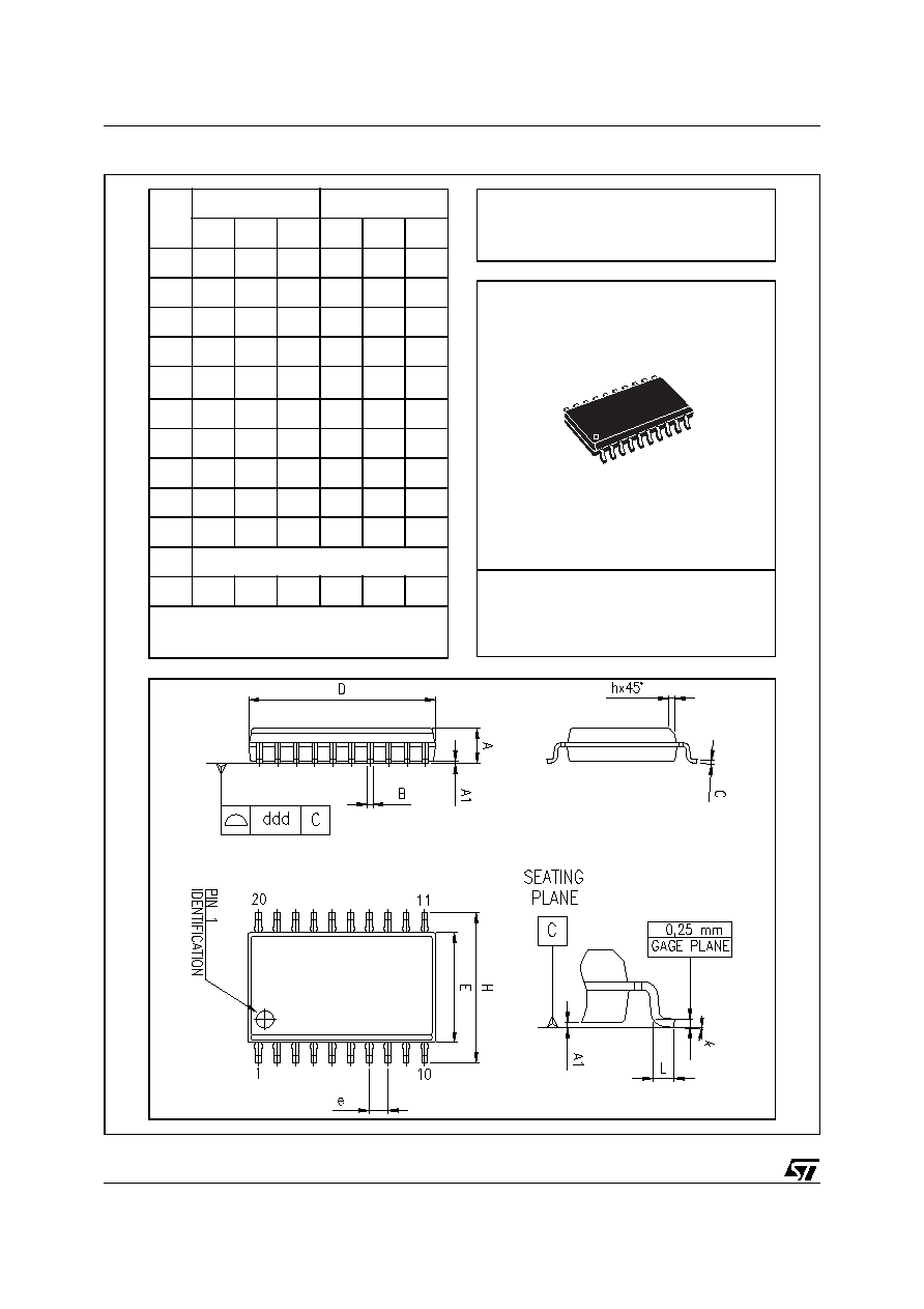
L4979MD L4979D
Figure 7. SO-8 Mechanical Data & Package Dimensions
OUTLINE AND
MECHANICAL DATA
DIM.
mm
inch
MIN.
TYP.
MAX.
MIN.
TYP.
MAX.
A
1.35
1.75
0.053
0.069
A1
0.10
0.25
0.004
0.010
A2
1.10
1.65
0.043
0.065
B
0.33
0.51
0.013
0.020
C
0.19
0.25
0.007
0.010
D
(1)
4.80
5.00
0.189
0.197
E
3.80
4.00
0.15
0.157
e
1.27
0.050
H
5.80
6.20
0.228
0.244
h
0.25
0.50
0.010
0.020
L
0.40
1.27
0.016
0.050
k
0į (min.), 8į (max.)
ddd
0.10
0.004
Note:
(1) Dimensions D does not include mold flash, protru-
sions or gate burrs.
Mold flash, potrusions or gate burrs shall not exceed
0.15mm (.006inch) in total (both side).
SO-8
0016023 C
L4979MD L4979D
8/10
Figure 8. SO-20 Mechanical Data & Package Dimensions
OUTLINE AND
MECHANICAL DATA
DIM.
mm
inch
MIN.
TYP.
MAX.
MIN.
TYP.
MAX.
A
2.35
2.65
0.093
0.104
A1
0.10
0.30
0.004
0.012
B
0.33
0.51
0.013
0.200
C
0.23
0.32
0.009
0.013
D
(1)
12.60
13.00
0.496
0.512
E
7.40
7.60
0.291
0.299
e
1.27
0.050
H
10.0
10.65
0.394
0.419
h
0.25
0.75
0.010
0.030
L
0.40
1.27
0.016
0.050
k
0į (min.), 8į (max.)
ddd
0.10
0.004
(1) "D" dimension does not include mold flash, protusions or gate
burrs. Mold flash, protusions or gate burrs shall not exceed
0.15mm per side.
SO20
0016022 D

9/10
L4979MD L4979D
Table 6. Revision History
Date
Revision
Description of Changes
June 2004
3
Changed the values of the parameter "Reset timing high/low threshold.
July 2004
4
Pin Connection SO-20 changed.
Changed some textes in the Features and table 2.
Changed some values in the tables 3, 4 and 5.
Changed some textes in the sections 2, 3 and 4.
October 2004
5
Changed from Product Preview to final datasheet.

Information furnished is believed to be accurate and reliable. However, STMicroelectronics assumes no responsibility for the consequences
of use of such information nor for any infringement of patents or other rights of third parties which may result from its use. No license is granted
by implication or otherwise under any patent or patent rights of STMicroelectronics. Specifications mentioned in this publication are subject
to change without notice. This publication supersedes and replaces all information previously supplied. STMicroelectronics products are not
authorized for use as critical components in life support devices or systems without express written approval of STMicroelectronics.
The ST logo is a registered trademark of STMicroelectronics.
All other names are the property of their respective owners
© 2004 STMicroelectronics - All rights reserved
STMicroelectronics GROUP OF COMPANIES
Australia - Belgium - Brazil - Canada - China - Czech Republic - Finland - France - Germany - Hong Kong - India - Israel - Italy - Japan -
Malaysia - Malta - Morocco - Singapore - Spain - Sweden - Switzerland - United Kingdom - United States
www.st.com
10/10
L4979MD - L4979D