 | –≠–ª–µ–∫—Ç—Ä–æ–Ω–Ω—ã–π –∫–æ–º–ø–æ–Ω–µ–Ω—Ç: L4981A | –°–∫–∞—á–∞—Ç—å:  PDF PDF  ZIP ZIP |
L4981A
L4981B
POWER FACTOR CORRECTOR
CONTROL BOOST PWM UP TO 0.99P.F.
LIMIT LINE CURRENT DISTORTION TO < 5%
UNIVERSAL INPUT MAINS
FEED FORWARD LINE AND LOAD REGULA-
TION
AVERAGE CURRENT MODE PWM FOR
MINIMUM NOISE SENSITIVITY
HIGH CURRENT BIPOLAR AND DMOS TO-
TEM POLE OUTPUT
LOW START-UP CURRENT (0.3mA TYP.)
UNDER VOLTAGE LOCKOUT WITH HYS-
TERESIS AND PROGRAMMABLE TURN ON
THRESHOLD
OVERVOLTAGE, OVERCURRENT PROTEC-
TION
PRECISE 2% ON CHIP REFERENCE EX-
TERNALLY AVAILABLE
SOFT START
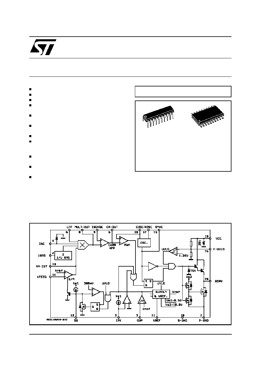
DESCRIPTION
The L4981 I.C. provides the necessary features
to achieve a very high power factor up to 0.99.
Realized in BCD 60II technology this power factor
corrector (PFC) pre-regulator contains all the con-
trol functions for designing a high efficiency-mode
power supply with sinusoidal line current con-
sumption.
The L4981 can be easily used in systems with
mains voltages between 85V to 265V without any
line switch. This new PFC offers the possibility to
work at fixed frequency (L4981A) or modulated
frequency (L4981B) optimizing the size of the in-
September 1998
Æ
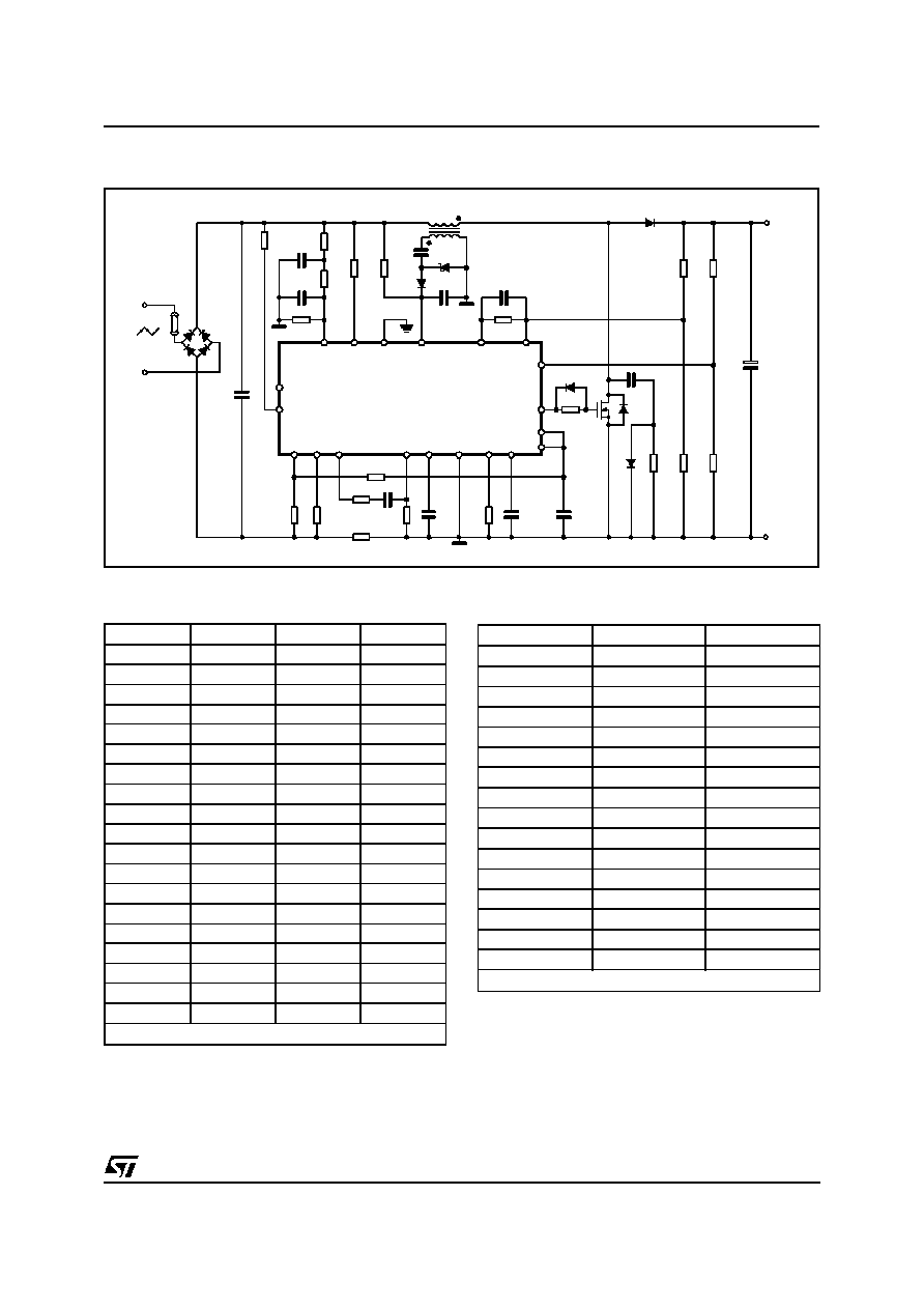
BLOCK DIAGRAM
ORDERING NUMBERS: L4981X (DIP20)
L4981XD (SO20)
DIP20
SO20
MULTIPOWER BCD TECHNOLOGY
1/17
put filter; both the operating frequency modes
working with an average current mode PWM con-
troller, maintaining sinusoidal line current without
slope compensation.
Besides power MOSFET gate driver, precise volt-
age reference (externally available), error ampli-
fier, undervoltage lockout, current sense and the
soft start are included. To limit the number of the
external components, the device integrates pro-
tections as overvoltage and overcurrent. The
overcurrent level can be programmed using a
simple resistor for L4981A. For a better precision
and for L4981B an external divider must be used.
ABSOLUTE MAXIMUM RATINGS
Symbol
Pin
Parameter
Value
Unit
V
CC
19
Supply Voltage (I
CC
50mA) (*)
selflimit
V
I
GDRV
20
Gate driv. output peak current (t = 1
µ
s)
SINK
2
.
SOURCE
1.5
A
V
GDRV
Gate driv. output voltage t = 0.1
µ
s
-1
V
Voltages at pins 3, 14, 7, 6, 12, 15
-0.3 to 9
V
V
VA-OUT
13
Error Amplifier Voltage
-0.3 to 8.5
V
I
AC
4
AC Input Current
5
mA
Voltages at pin 8, 9
-0.5 to 7
V
V
CA-OUT
5
Current Amplifier Volt. (Isource = -20mA; Isink = 20mA)
-0.3 to 8.5
V
V
ROSC
17
Voltage at pin 17
-0.3 to 3
V
11, 18
Voltage at pin 11, 18
-0.3 to 7
V
I
COSC
18
Input Sink Current
15
mA
I
FREQ-MOD
16
Frequency Modulation Sink Current (L4981B)
5
mA
V
SYNC
16
Sync. Voltage (L4981A)
-0.3 to 7
V
V
IPK
2
Voltage at pin 2
Voltage at Pin 2 t = 1
µ
s
-0.3 to 5.5
-2
V
V
P
tot
Power Dissipation at T
amb
= 70
∞
C
(DIP20)
1
W
Power Dissipation at T
amb
= 70
∞
C
(SO20)
0.6
W
T
op
Operating Ambient Temperature
-40 to 125
∞
C
T
stg
StorageTemperature
-55 to 150
∞
C
(*) Maximum package power dissipation limits must be observed.
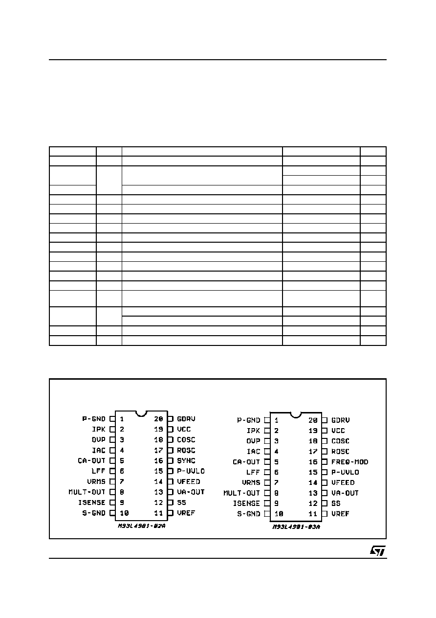
PIN CONNECTIONS (Top views)
L4981A
L4981B
L4981A - L4981B
2/17
THERMAL DATA
Symbol
Parameter
DIP 20
SO 20
Unit
R
th j-amb
Thermal Resistance Junction-ambient
80
120
∞
C/W
PIN FUNCTIONS
N.
Name
Description
1
P-GND
Power ground.
2
IPK
L4981A peak current limiting. A current limitation is obtained using a single resistor connected
between Pin 2 and the sense resistor. To have a better precision another resistor between Pin
2 and a reference voltage (Pin 11) must be added.
L4981B peak current limiting. A precise current limitation is obtained using two external
resistor only. These resistors must be connected between the sense resistor, Pin 2 and the
reference voltage.
3
OVP
Overvoltage protection. At this input are compared an internal precise 5.1V (typ) voltage
reference with a sample of the boost output voltage obtained via a resistive voltage divider in
order to limit the maximum output peak voltage.
4
IAC
Input for the AC current. An input current proportional to the rectified mains voltage generates,
via a multiplier, the current reference for the current amplifier.
5
CA-OUT
Current amplifier output. An external RC network determinates the loop gain.
6
LFF
Load feedforward; this voltage input pin allows to modify the multiplier output current
proportionally to the load, in order to give a faster response versus load transient. The best
control is obtained working between 1.5V and 5.3V. If this function is not used, connect this pin
to the voltage reference (pin = 11).
7
VRMS
Input for proportional RMS line voltage. the VRMS input compesates the line voltage changes.
Connecting a low pass filter between the rectified line and the pin 7, a DC voltage proportional
to the input line RMS voltage is obtained. The best control is reached using input voltage
between 1.5V and 5.5V. If this function is not used connect this pin to the voltage reference
(pin = 11).
8
MULT-OUT
Multiplier output. This pin common to the multiplier output and the current amplifier N.I. input is
an high impedence input like I
SENSE
. The MULT-OUT pin must be taken not below -0.5V.
9
I
SENSE
Current amplifier inverting input. Care must be taken to avoid this pin goes down -0.5V.
10
S-GND
Signal ground.
11
V
REF
Output reference voltage (typ = 5.1V).Voltage refence at
±
2% of accuracy externally available,
it's internally current limited and can deliver an output current up to 10mA.
12
SS
A capacitor connected to ground defines the soft start time. An internal current generator
delivering 100
µ
A (typ) charges the external capacitor defining the soft start time constant. An
internal MOS discharge, the external soft start capacitor both in overvoltage and UVLO
conditions.
13
VA-OUT
Error amplifier output, an RC network fixes the voltage loop gain characteristics.
14
VFEED
Voltage error amplifier inverting input. This feedback input is connected via a voltage divider to
the boost output voltage.
15
P-UVLO
Programmable under voltage lock out threshold input. A voltage divider between supply
voltage and GND can be connected in order to program the turn on threshold.
16
SYNC
(L4981A)
This synchronization input/output pin is CMOS logic compatible. Operating as SYNC in, a
rectangular wave must be applied at this pin. Opearting as SYNC out, a rectangular clock
pulse train is available to synchronize other devices.
FREQ-MOD
(L4981B)
Frequency modulation current input. An external resistor must be connected between pin 16
and the rectified line voltage in order to modulate the oscillator frequency. Connecting pin 16 to
ground a fixed frequency imposed by R
OSC
and C
OSC
is obtained.
17
R
OSC
An external resistor connected to ground fixes the constant charging current of C
OSC
.
18
C
OSC
An external capacitor connected to GND fixes the switching frequency.
19
V
CC
Supply input voltage.
20
GDRV
Output gate driver. Bipolar and DMOS transistors totem pole output stage can deliver peak
current in excess 1A useful to drive MOSFET or IGBT power stages.
L4981A - L4981B
3/17
ELECTRICAL CHARACTERISTICS (Unless otherwise specified V
CC
= 18V, C
OSC
= 1nF,
R
OSC
= 24K
, C
SS
= 1
µ
F, V
CA-OUT
= 3.5V, V
ISENSE
= 0V, V
LFF
= V
REF
, I
AC
= 100
µ
A, V
RMS
= 1V,
V
FEED
= GND, V
IPK
= 1V, V
OVP
= 1V, T
J
= 25
∞
C
Symbol
Prameter
Test Condition
Min.
Typ.
Max.
Unit
ERROR AMPLIFIER SECTION
V
IO
Input Offset Voltage
≠25
∞
C < T
J
< 85
∞
C
±
8
mV
I
IB
Input Bias Current
V
FEED
= 0V
-500
-50
500
nA
Open Loop Gain
70
100
dB
V
13H
Output High voltage
V
FEED
= 4.7V
I
VA-OUT
= -0.5mA
5.5
6.5
7.5
V
V
13L
Output Low Voltage
V
FEED
= 5.5V
I
VA-OUT
= 0.5mA
0.4
1
V
-I
13
Output Source Current
V
FEED
= 4.7V; V
VA-OUT
= 3.5V
2
10
mA
I
13
Output Sink Current
V
FEED
= 5.5V; V
VA-OUT
= 3.5V
4
20
mA
REFERENCE SECTION
V
ref
Reference Output Voltage
≠25
∞
C < T
J
< 85
∞
C
4.97
5.1
5.23
V
T
j
= 25
∞
C I
ref
= 0
5.01
5.1
5.19
V
V
ref
Load Regulation
1mA
I
ref
10mA
≠25
∞
C < T
J
< 85
∞
C
3
15
mV
V
ref
Line Regulation
12V
V
CC
19V
≠25
∞
C < T
J
< 85
∞
C
3
10
mV
I
ref sc
Short Circuit Current
V
ref
= 0V
20
30
50
mA
OSCILLATOR SECTION
f
osc
Initial Accuracy
T
j
= 25
∞
C
85
100
115
KHz
Frequency Stability
12V
V
CC
19V
≠25
∞
C < T
J
< 85
∞
C
80
100
120
KHz
V
svp
Ramp Valley to Peak
4.7
5
5.3
V
I
18C
Charge Current
V
COSC
= 3.5V
0.45
0.55
0.65
mA
I
18D
Discharge Current
V
COSC
= 3.5V
11.5
mA
V
18
Ramp Valley Voltage
0.9
1.15
1.4
V
SYNC SECTION (Only for L4981A)
t
W
Output Pulse Width
50% Amplitude
0.3
0.8
µ
s
I
16
Sink Current with Low Output
Voltage
V
SYNC
= 0.4V
V
COSC
= 0V
0.4
0.8
mA
-I
16
Source Current with High Output
Voltage
V
SYNC
= 4.5V
V
COSC
= 6.7V
1
6
mA
V
16L
Low Input Voltage
0.9
V
V
16H
High Input Voltage
3.5
V
t
d
Pulse for Synchronization
800
ns
FREQUENCY MODULATION FUNCTION (Only for L4981B)
f
18max
Maximum Oscillation Frequency
V
FREQ-MOD
= 0V (Pin 16) I
freq
= 0
85
100
115
KHz
f
18min
Minimum Oscillator Frequency
I
FREQ-MOD
= 360
µ
A (Pin 16)
V
VRMS
= 4V (Pin 7)
74
KHz
I
FREQ-MOD
= 180
µ
A (Pin 16)
V
VRMS
= 2V (Pin 7)
76
KHz
SOFT START SECTION
I
SS
Soft Start Source Current
V
SS
= 3V
60
100
140
µ
A
V
12sat
Output Saturation Voltage
V
3
= 6V, I
SS
= 2mA
0.1
0.25
V
L4981A - L4981B
4/17

ELECTRICAL CHARACTERISTICS (continued)
Symbol
Parameter
Test Condition
Min.
Typ.
Max.
Unit
SUPPLY VOLTAGE
V
CC
Operating Supply Voltage
19.5
V
OVER VOLTAGE PROTECTION COMPARATOR
V
thr
Rising Threshold Voltage
V
ref
-20mV
5.1
V
ref
+20mV
V
V
3Hys
Hysteresis
180
250
320
mV
I
3
Input Bias Current
0.05
1
µ
A
t
d
Propagation delay to output
V
OVP
= V
thr
+100mV
1
2
µ
s
OVER CURRENT PROTECTION COMPARATOR
V
th
Threshold Voltage
±
30
mV
t
d
Propagation delay to Output
V
OCP
= V
thr
-0.2V
0.4
0.9
µ
s
I
ipk
Current Source Generator
V
IPK
= -0.1V
only for L4981A
65
85
105
µ
A
I
L
Leakage Current
V
IPK
= -0.1V
only for L4981B
5
µ
A
CURRENT AMPLIFIER SECTION
V
offset
Input Offset Voltage
V
MULT OUT
= V
SENSE
= 3.5V
±
2
mV
I
9bias
Input Bias Current
V
SENSE
= 0V
-500
50
500
nA
Open Loop Gain
1.1V
V
CA OUT
6V
70
100
dB
SVR
Supply Voltage Rejection
12V
V
CC
19V
V
MULT OUT
= 3.5V V
SENSE
= 3.5V
68
90
dB
V
5H
Output High Voltage
V
MULT OUT
= 200mV
I
CA OUT
= -0.5mA, V
IAC
= 0V
6.2
V
V
5L
Output Low Voltage
V
MULT OUT
= -200mV
I
CA OUT
= 0.5mA, V
IAC
= 0V
0.9
V
-I
5
Output Source Current
V
MULT OUT
= 200mV,
V
IAC
= 0V, V
CA-OUT
= 3.5V
2
10
mA
I
5
Output Sink Current
2
10
mA
OUTPUT SECTION
V
20L
Output Voltage Low
I
SINK
= 250mA
0.5
0.8
V
V
20H
Output Voltage High
I
SOURCE
= 250mA
V
CC
= 15V
11.5
12.5
V
t
r
Output Voltage Rise Time
C
OUT
= 1nF
50
150
ns
t
f
Output Voltage Fall Time
C
OUT
= 1nF
30
100
ns
V
GDRV
Voltage Clamp
I
SOURCE
= 0mA
13
16
19
V
TOTAL STANDBY CURRENT SECTION
I
19start
Supply Current before start up
V
CC
= 14V
0.3
0.5
mA
I
19on
Supply Current after turn on
V
IAC
= 0V, V
COSC
= 0,
Pin17 = Open
8
12
mA
I
19
Operating Supply Current
Pin20 = 1nF
12
16
mA
V
CC
Zener Voltage
(*)
20
25
30
V
UNDER VOLTAGE LOCKOUT SECTION
V
th ON
Turn on Threshold
14.5
15.5
16.5
V
V
th OFF
Turn off Threshold
9
10
11
V
Programmable Turn-on Threshold
Pin 15 to V
CC
= 220K
Pin15 to GND = 33K
10.6
12
13.4
V
LOAD FEED FORWARD
I
LFF
Bias Current
V
6
= 1.6V
70
140
µ
A
V
6
= 5.3V
200
300
µ
A
V
I
Input Voltage Range
1.6
5.3
V
(*) Maximum package power dissipation limits must be observed.
L4981A - L4981B
5/17

ELECTRICAL CHARACTERISTICS (continued)
Symbol
Prameter
Test Condition
Min.
Typ.
Max.
Unit
MULTIPLIER SECTION
Multipler Output Current
V
VA-OUT
= 4V, V
RMS
= 2V,
V
MULTOUT
= 0, V
LFF
= 5.1V
I
AC
= 50
µ
A, C
OSC
= 0V
20
35
52
µ
A
V
VA-OUT
= 4V, V
RMS
= 2V,
V
MULTOUT
= 0, V
LFF
= 5.1V
I
AC
= 200
µ
A, C
OSC
= 0V
100
135
170
µ
A
V
VA-OUT
= 2V, V
RMS
= 2V,
V
MULTOUT
= 0, V
LFF
= 5.1V
I
AC
= 100
µ
A, C
OSC
= 0V
10
20
30
µ
A
V
VA-OUT
= 2V, V
RMS
= 4V,
V
MULTOUT
= 0, V
LFF
= 5.1V
I
AC
= 100
µ
A, C
OSC
= 0V
2
5.5
11
µ
A
V
VA-OUT
= 4V, V
RMS
= 4V,
V
MULTOUT
= 0, V
LFF
= 5.1V
I
AC
= 100
µ
A, C
OSC
= 0V
10
22
34
µ
A
V
VA-OUT
= 4V, V
RMS
= 2V,
V
MULTOUT
= 0, V
LFF
= 2.5V
C
OSC
= 0V, I
AC
= 200
µ
A
20
37
54
µ
A
V
VA-OUT
= 4V, V
RMS
= 4V
V
MULTOUT
= 0, V
LFF
= 5.1V
I
AC
= 200
µ
A, C
OSC
= 0V
20
39
54
µ
A
V
VA-OUT
= 2V, V
RMS
= 4V,
V
MULTOUT
= 0, V
LFF
= 5.1V
I
AC
= 0, C
OSC
= 0V
-2
0
2
µ
A
K
Multiplier Gain
0.37
I
MULT
-
OUT
=
K
I
AC
(
V
VA
-
OUT
-
1.28
) (
0.8
V
LFF
-
1.28
)
(
V
VRMS
)
2
if V
LFF
= V
REF;
I
MULT
-
OUT
=
I
AC
(
V
VA
-
OUT
-
1.28
)
(
V
VRMS
)
2
K1
where: K1 = 1V
Figure 1: MULTI-OUT vs. I
AC
(V
RMS
= 1.7V;
V
LFFD
= 5.1V)
Figure 2: MULTI-OUT vs. I
AC
(V
RMS
= 2.2V;
V
LFFD
= 5.1V)
L4981A - L4981B
6/17
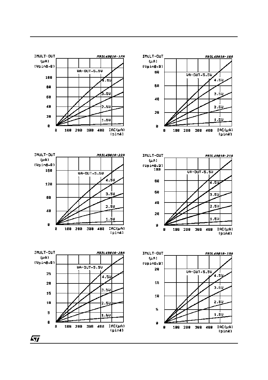
Figure 3: MULTI-OUT vs. I
AC
(V
RMS
= 4.4V;
V
LFFD
= 5.1V)
Figure 4: MULTI-OUT vs. I
AC
(V
RMS
= 5.3V;
V
LFFD
= 5.1V)
Figure 6: MULTI-OUT vs. I
AC
(V
RMS
= 2.2V;
V
LFFD
= 2.5V)
Figure 5: MULTI-OUT vs. I
AC
(V
RMS
= 1.7V;
V
LFFD
= 2.5V)
Figure 7: MULTI-OUT vs. I
AC
(V
RMS
= 4.4V;
V
LFFD
= 2.5V)
Figure 8: MULTI-OUT vs. I
AC
(V
RMS
= 5.3V;
V
LFFD
= 2.5V)
L4981A - L4981B
7/17

C7
C8
R8
R7
R6
R14
7
4
BRIDGE
C1
L4981A
15
16
R15
19
C12
D4
D3
C5
T
13
14
C9
R12
3
C11
R13
MOS
D5
R17
20
R11
R3
R5
C3
R4
C4
R16
C6
C10
1
R2
R10
R1
R9
D1
6
11
12
17
10
18
9
5
8
2
FUSE
Vi
C2
+
-
Vo=400V
D93IN029B
85VAC-265VAC
D2
RS
R21
Figure 9A: L4981A Power Factor Corrector (200W)
C1
470nF
400V
C2
100
µ
F
450V
C3
2.2nF
C4
1nF
C5
100
µ
F
25V
C6
1
µ
F
16V
C7
220nF
63V
C8
220nF
63V
C9
330nF
C10
1
µ
F
16V
C11
270pF
400V
C12
8.2nF
100V
D1
STTA506D
D2, D3
1N4148
D4
18V
1/2W
D5
BYT11-600
MOS
STH/STW15NA50
FUSE = 4A/250V
R
S
0.07(3 x .22)
1/2W
5%
R1
820k
1/4W
1%
R2
10k
1/4W
1%
R3
1.8k
1/4W
5%
R4
1.8k
1/4W
5%
R5
18k
1/4W
5%
R6
1.2M
1/4W
5%
R7
360k
1/4W
5%
R8
33k
1/4W
5%
R9
1.8M
1/4W
1%
R10
21k
1/4W
1%
R11
402
1/4W
1%
R12
120k
1/4W
5%
R13
27
1/4W
5%
R14
1M
1/4W
1%
R15
120k
1/2W
5%
R16
30k
1/4W
5%
R17
1.8k
4W
1%
R21
5.1k
1/4W
1%
BRIDGE = 4 x P600M
PART LIST
T= primary: 88 turns of 12 x 32 AWG (0.2mm)
secondary: 9 turns of # 27AWG (0.15mm)
core: B1ET3411A THOMSON - CSF
gap: 1,6mm for a total primary inductance of
0.9mH
f
SW
= 80kHz P
O
= 200W
V
OUT
= 400V I
rms max
= 2.53A
V
OVP
= 442V I
PK max
= 6.2A
L4981A - L4981B
8/17
C7
C8
R8
R7
R6
R14
7
4
BRIDGE
C1
L4981B
15
16
R15
19
C12
D4
D3
C5
T
13
14
C9
R12
3
C11
R13
MOS
D5
R17
20
R11
R3
R5
C3
R4
C4
R16
C6
C10
1
R2
R10
R1
R9
D1
6
11
12
17
10
18
9
5
8
2
FUSE
Vi
C2
+
-
Vo=400V
D95IN220
85VAC-265VAC
D2
RS
R21
R22
Figure 9B: L4981B Power Factor Corrector (200W)
C1
470nF
400V
C2
100
µ
F
450V
C3
2.2nF
C4
1.1nF
C5
100
µ
F
25V
C6
1
µ
F
16V
C7
220nF
63V
C8
220nF
63V
C9
330nF
C10
1
µ
F
16V
C11
270pF
400V
C12
8.2nF
100V
D1
STTA506D
D2, D3
1N4148
D4
18V
1/2W
D5
BYT11-600
MOS
STH/STW15NA50
FUSE = 4A/250V
R
S
0.07(3 x .22)
1/2W
5%
R1
820k
1/4W
1%
R2
10k
1/4W
1%
R3
1.8k
1/4W
5%
R4
1.8k
1/4W
5%
R5
18k
1/4W
5%
R6
1.2M
1/4W
5%
R7
360k
1/4W
5%
R8
33k
1/4W
5%
R9
1.8M
1/4W
1%
R10
21k
1/4W
1%
R11
402
1/4W
1%
R12
120k
1/4W
5%
R13
27
1/4W
5%
R14
1M
1/4W
1%
R15
120k
1/2W
5%
R16
24k
1/4W
5%
R17
1.8k
4W
1%
R21
5.1k
1/4W
1%
R22
1.1M
1/4W
1%
BRIDGE = 4 x P600M
PART LIST
T= primary: 88 turns of 12 x 32 AWG (0.2mm)
secondary: 9 turns of # 27AWG (0.15mm)
core: B1ET3411A THOMSON - CSF
gap: 1,6mm for a total primary inductance of
0.9mH
f
SW
= 80 to 92kHz P
O
= 200W
V
OUT
= 400V I
rms max
= 2.53A
V
OVP
= 442V I
PK max
= 6.2A
L4981A - L4981B
9/17

Figure 10: Reference Voltage vs. Source Refer-
ence Current
Figure 12: Reference Voltage vs. Junction Tem-
perature
Figure 14: Gate Driver Rise and Fall Time
Figure 11: Reference Voltage vs. Supply Voltage
Figure 13: Switching Frequency vs. Junction
Temperature
Figure 15: Operating Supply Current vs. Supply
Voltage
L4981A - L4981B
10/17

Figure 16: Programmable Under Voltage Lock-
out Thresholds
Table 1: Programmable Under Voltage Lockout Thresholds.
V
CC ON
V
CC OFF
R22
R23
11V
10V
82k
12k
12V
10.1V
220k
33k
13V
10.5V
430k
62k
14V
10.8V
909k
133k
14.5V
10.9V
1.36M
200k
15V
11V
2.7M
390k
Vl
0.8
1
0.4
0.2
0
0
45
90
135
Electrical degrees
180
0.8
1
0.4
0.2
0
fsw
Figure 17: Modulation Frequency Normalized in
an Half Cycle of the Mains Voltage
Figure 18: Oscillator Diagram
R22 = R23
6.8
R23 (Kohm)
L4981A - L4981B
11/17
Figure 19: 200W Evaluation Board Circuit.
T= primary: 75 turns of litz wire 20 x 32 AWG (0.2mm)
secondary: 8 turns of # 27AWG (0.15mm)
core: B1ET3411A THOMSON - CSF
gap: 1.4mm for a total primary inductance of 0.7mH
f
sw
= 100kHz; V
O
= 400V;
P
O
= 200W
NOTE:
Start Up Circuit
Usually the V
CC
capacitor (C11 in fig. 19) can be charged by a resistor
drawing current from the rectified mains. In the evaluation board
instead the start up circuit composed by (Q2+R19+R15+Dz) has
been designed to perform a fast and effective supply in all the
conditions. Once that the L4981A/B has started, the reference
voltage available at pin 6 by R20 and Q3, ensures Q2 to be turned
off.
Programmable Under voltage Lockout
The PCB allows to insert a couple of resistor (R22, R23) to modify
the threshold input voltage. Please refer to fig. 16 and table1.
L4981A - L4981B
12/17
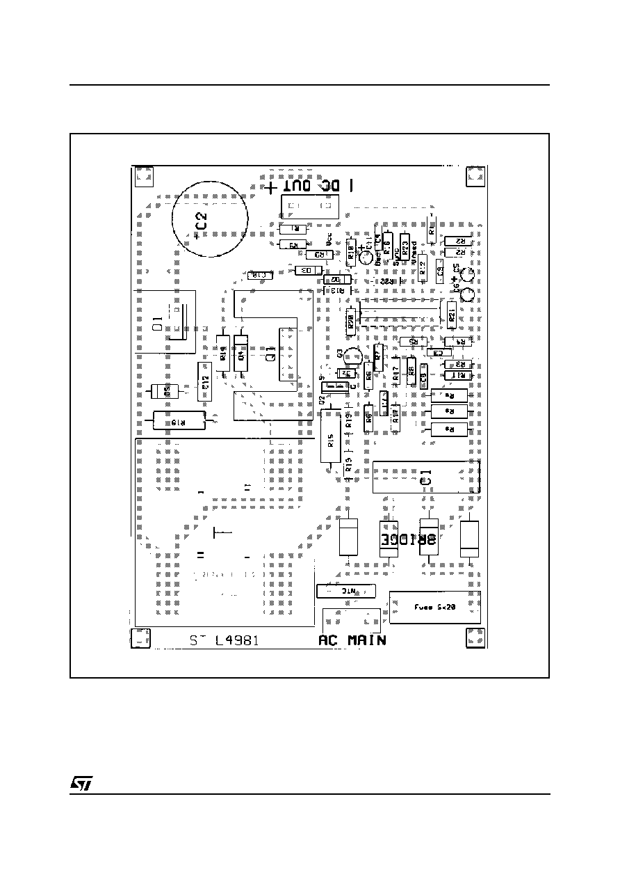
Figure 20: P.C. Board and Component Layout of Evaluation Board Circuit (1:1 scale).
L4981A - L4981B
13/17
The evaluation board has been designed using: a
faster not dissipative start-up circuit, a diode (D2)
to speed-up the MOS start-off time and (even if a
single resistor can be used) an external divider to
improve the precision of the overcurrent thresh-
old.
Further there is a possibility to change the input
threshold voltage using an external divider (R23
and R22) and if an inrush current problem arises
a NTC resistor can be used.
The PFC demoboard performances has been
evaluated testing the following parameters:
PF (power factor), A-THD (percentage of current
total harmonic distortion), H3..H9 (percentage of
current's n
th
harmonic amplitude),
V
o
(output
voltage ripple), V
o
(output voltage),
(efficiency).
The test configuration, equipments and results
are:
AC POWER
SOURCE
LARCET /3KW
PM1200
AC POWER
ANALYSER
EMI
FILTER
PFC
L4981
DEMO
LOAD
D94IN057
V
i
f
P
i
PF
A-THD
H3
H5
H7
H9
V
O
V
O
PO
(V
rms
)
(Hz)
(W)
(%)
(%)
(%)
(%)
(%)
(V)
(V)
(W)
(%)
88
60
222
0.999
2.94
1.98
0.61
0.55
0.70
390
8
200
90.2
110
60
220
0.999
1.79
1.40
0.40
0.31
0.28
392
8
201
91.6
132
60
218
0.999
1.71
1.16
0.40
0.35
0.31
394
8
202
92.8
180
50
217
0.999
1.88
1.52
0.65
0.40
0.34
396
8
203
93.8
220
50
217
0.997
2.25
1.68
0.83
0.57
0.48
398
8
204
94.2
260
50
216
0.995
3.30
1.84
1.30
0.39
0.73
400
8
205
95.2
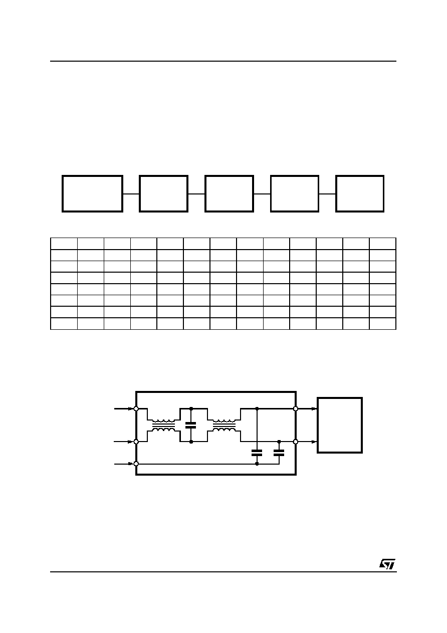
EMI/RFI FILTER
The harmonic content measurement has been
done using an EMI/RFI filter interposed between
the AC source and the demoboard under test,
while the efficiency has been calculated without
the filter contribution.
C1
D94IN052
T1
T2
C
LINE
PFC
EARTH
where:
T1 = 1mH
C1 = 0.33
µ
F, 630V
T2 = 27mH
C2 = 2.2nF, 630V
L4981A - L4981B
14/17
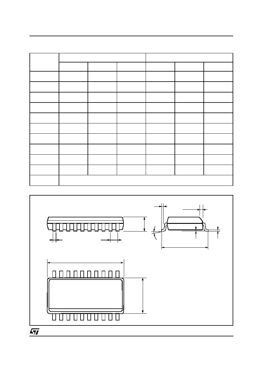
SO20 PACKAGE MECHANICAL DATA
DIM.
mm
inch
MIN.
TYP.
MAX.
MIN.
TYP.
MAX.
A
2.35
2.65
0.093
0.104
A1
0.1
0.3
0.004
0.012
B
0.33
0.51
0.013
0.020
C
0.23
0.32
0.009
0.013
D
12.6
13
0.496
0.512
E
7.4
7.6
0.291
0.299
e
1.27
0.050
H
10
10.65
0.394
0.419
h
0.25
0.75
0.010
0.030
L
0.4
1.27
0.016
0.050
K
0 (min.)8 (max.)
1
10
11
20
A
e
B
D
E
L
K
H
A1
C
SO20MEC
h x 45
∞
L4981A - L4981B
15/17
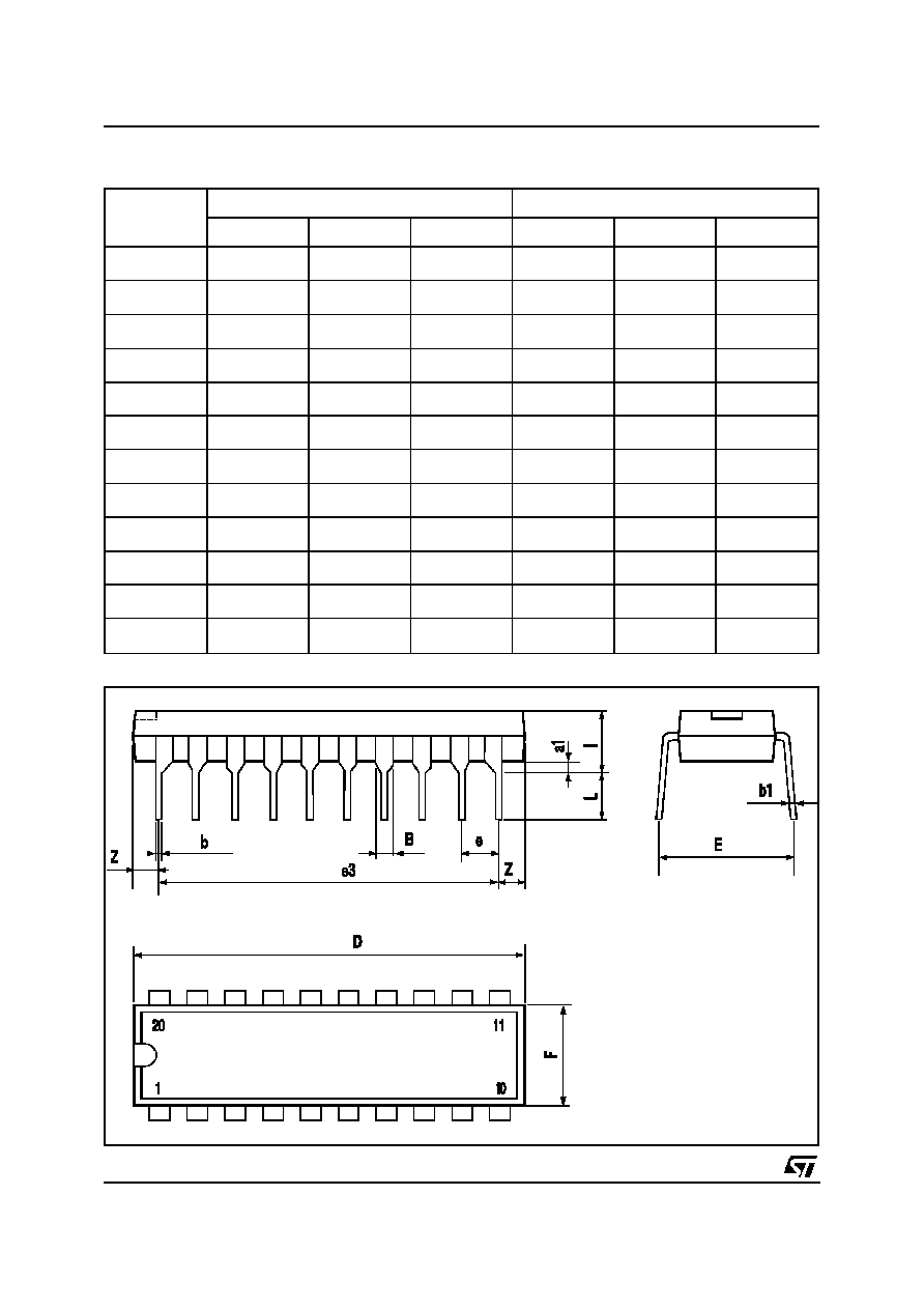
DIP20 PACKAGE MECHANICAL DATA
DIM.
mm
inch
MIN.
TYP.
MAX.
MIN.
TYP.
MAX.
a1
0.254
0.010
B
1.39
1.65
0.055
0.065
b
0.45
0.018
b1
0.25
0.010
D
25.4
1.000
E
8.5
0.335
e
2.54
0.100
e3
22.86
0.900
F
7.1
0.280
I
3.93
0.155
L
3.3
0.130
Z
1.34
0.053
L4981A - L4981B
16/17

Information furnished is believed to be accurate and reliable. However, STMicroelectronics assumes no responsibility for the consequences
of use of such information nor for any infringement of patents or other rights of third parti es which may result from its use. No license is
granted by implication or otherwise under any patent or patent rights of STMicroelectronics. Specification mentioned in this publication are
subject to change without notice. This publication supersedes and replaces all information previously supplied. STMicroelectronics products
are not authorized for use as critical components in life support devices or systems without express written approval of STMicroelectronics.
The ST logo is a registered trademark of STMicroelectronics
©
1998 STMicroelectronics ≠ Printed in Italy ≠ All Rights Reserved
STMicroelectronics GROUP OF COMPANIES
Australia - Brazil - Canada - China - France - Germany - Italy - Japan - Korea - Malaysia - Malta - Mexico - Morocco - The Netherlands -
Singapore - Spain - Sweden - Switzerland - Taiwan - Thailand - United Kingdom - U.S.A.
L4981A - L4981B
17/17