 | –≠–ª–µ–∫—Ç—Ä–æ–Ω–Ω—ã–π –∫–æ–º–ø–æ–Ω–µ–Ω—Ç: L4989D | –°–∫–∞—á–∞—Ç—å:  PDF PDF  ZIP ZIP |

1/10
L4989
March 2004
This is preliminary information on a new product now in development. Details are subject to change without notice.
OPERATING DC SUPPLY VOLTAGE RANGE
5.6V TO 31V
VERY LOW QUIESCENT CURRENT WITH
WATCHDOG DISABLED
PRECISION OUTPUT VOLTAGE (3%)
LOW-DROP VOLTAGE
(180mV typ at I
o
= 150mA)
RESET CIRCUIT SENSING THE OUTPUT
VOLTAGE DOWN TO 1V
PROGRAMMABLE RESET DELAY WITH
EXTERNAL CAPACITOR
WATCHDOG DISABLE INPUT
PROGRAMMABLE WATCHDOG TIMER WITH
EXTERNAL CAPACITOR
THERMAL SHUTDOWN AND SHORT
CIRCUIT PROTECTION
WIDE TEMPERATURE RANGE (T
j
= -40∞C TO
150∞C)
ORDERING NUMBERS: L4989D (SO8)
L4989 (SO20)
SO20
SO8
PRODUCT PREVIEW
LOW POWER VOLTAGE REGULATOR
BLOCK DIAGRAMt
watchdog
Vs
Vi
Wi
Vcw
Vcr
Ctr
Ctw
Res
WE
gnd
Vo
Co
Voltage
Reference
Reset
Start up
100mV
+
_
1.25V
watchdog
Vs
Vi
Wi
Vcw
Vcr
Ctr
Ctw
Res
WE
gnd
Vo
Co
Voltage
Reference
Reset
Start up
100mV
+
_
1.25V

L4989
2/10
PIN DESCRIPTION
PIN CONNECTIONS
N. (SO8)
N. (SO20)
NAME
FUNCTION
1
1
WEn
Watchdog enable input.
If high it activates the watchdog operation.
2
4
gnd
Ground reference
5,6,15,16
gnd
Ground
Connected these pins to a heat spreader ground
3
7
Res
Reset output.
It is pulled down when output voltage goes below Vo_th or
frequency at Wi is too low.
4
10
Vcr
Reset timing adjust.
A capacitor between Vcr pin and gnd, sets the reset delay time
(trd)
5
11
Vcw
Watchdog timer adjust
A capacitor between Vcw pin and gnd, sets the time response of
the watchdog monitor.
6
14
Wi
Watchdog input.
If the frequency at this input pin is too low, the Reset output is
activated.
7
17
Vo
Voltage regulator output
Block to ground with a capacitor >100nF (needed for regulator
stability)
8
20
Vs
Supply voltage
Block to ground directly at IC pin with a ceramic capacitor
2,3,8,9,12,
13,18,19
N. C.
not connected
V
EN
GND
RES
V
CR
V
CW
W
I
V
O
V
S
1
3
2
4
6
5
7
8
D04AT515
V
EN
N.C.
N.C.
GND
GND
RES
GND
N.C.
N.C.
N.C.
N.C.
W
I
GND
GND
V
O
N.C.
N.C.
V
S
1
3
2
4
5
6
7
8
9
18
17
16
15
14
12
13
11
19
10
20
V
CR
W
CW
D04AT516
SO8
SO20

3/10
L4989
ABSOLUTE MAXIMUM RATINGS
Note:
Maximum ratings are absolute ratings; exceeding any one of these values may cause perma-nent damage to the integrated circuit.
THERMAL DATA
(*) with 6 sq. cm on board heat sink
ELECTRICAL CHARACTERISTICS (Vs = 5.6V to 31V, Tj = -40∞C to +150∞C unless otherwise specified)
Symbol
Parameter
Value
Unit
V
Vsdc
DC supply voltage
-0.3 to 40
V
I
Vsdc
Input current
internally limited
V
Vo
DC output voltage
-0.3 to 6
V
I
Vo
DC output current
internally limited
V
Wi
Watchdog input voltage
-0.3 to VVo + 0.3
V
V
od
Open drain output voltage (RES)
-0.3 to VVo + 0.3
V
I
od
Open drain output current (RES)
internally limited
V
cr
Reset delay voltage
-0.3 to VVo + 0.3
V
V
cw
Watchdog delay voltage
-0.3 to VVo + 0.3
V
V
WEn
Watchdog enable input
-0.3 to 40
V
T
j
Junction temperature
-40 to 150
∞C
V
ESD
ESD voltage level (HBM-MIL STD 883C)
±
2
kV
Symbol
Parameter
SO8
SO12+4+4
Unit
R
th-j amb
Thermal Resistance Junction to ambient
130 to 180
50(*)
∞C/W
Pin
Symbol
Parameter
Test Condition
Min.
Typ.
Max.
Unit
GENERAL
Vo
V
o_ref
Output voltage
Vs=5.6 to 31V
Io=1 to 150mA
4.85
5.00
5.15
V
Vo
I
short_13
Short circuit current (1)
Vs=13.5V
160
210
250
mA
Vo
I
lim
Output current limitation (1)
Vs=13.5V
170
250
290
mA
Vs, Vo
V
line
Line regulation voltage
Vs=5.6 to 31V
Io=1 to 150mA
25
mV
Vo
V
load
Load regulation voltage
Io=1 to 150mA
25
mV
Vs, Vo
V
dp
Drop voltage
Io=150mA
180
400
mV
Vs, Vo
SVR
Ripple rejection
fr = 100 Hz
55
dB
Vs, Vo
I
qs_1
Current consumption
with watchdog not active
I
qs_1
= I
Vs
≠ I
o
Vs=13.5V, Io<1mA,
WEn low
69
115
µ
A

L4989
4/10
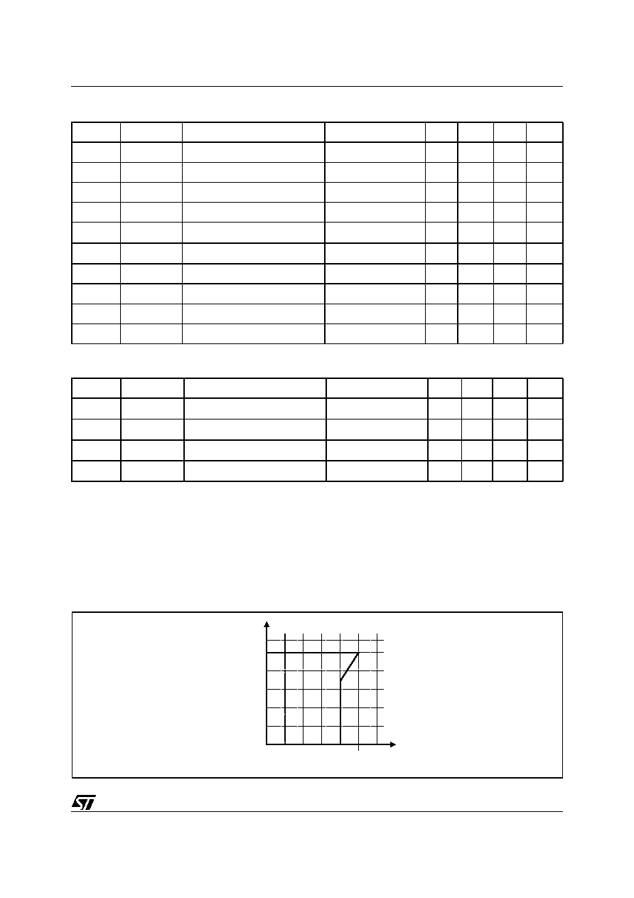
Note: 1. see fig1 (behavior of output current versus regulated voltage Vo)
RESET
2. When Vo becomes lower than 4V, the reset reaction time decreases down to 2 s assuring a faster reset condition in this particular
case.
Vs, Vo
I
qs_10
Current consumption
with watchdog not active
I
qs_10
= I
Vs
≠ I
o
Vs=13.5V,
Io=10mA,
WEn low
127
300
µ
A
Vs, Vo
I
qs_50
Current consumption
with watchdog not active
I
qs_50
= I
Vs
≠ I
o
Vs=13.5V, Io=50mA,
WEn low
498
900
µ
A
Vs, Vo
I
qs_150
Current consumption
with watchdog not active
I
qs_150
= I
Vs
≠ I
o
Vs=13.5V, Io=150mA,
WEn low
1.40
2
mA
Vs, Vo
I
qn_1
Current consumption
with watchdog active
I
qn_1
= I
Vs
≠ I
o
Vs=13.5V, Io<1mA,
WEn high
110
170
µ
A
Vs, Vo
I
qn_10
Current consumption
with watchdog active
I
qn_10
= I
Vs
≠ I
o
Vs=13.5V,
Io=10mA,
WEn high
168
350
µ
A
Vs, Vo
I
qn_50
Current consumption
with watchdog active
I
qn_50
= I
Vs
≠ I
o
Vs=13.5V,
Io=50mA,
WEn high
538
1000
µ
A
Vs, Vo
I
qn_150
Current consumption
with watchdog active
I
qn_150
= I
Vs
≠ I
o
Vs=13.5V,
Io=150mA,
WEn high
1.45
2.00
mA
Tw
Thermal protection temperature
150
190
∞C
Tw_hy
Thermal protection temperature
hysteresis
10
∞C
Pin
Symbol
Parameter
Test condition
min
typ
max
Unit
Res
Vres_l
Reset output low voltage
Rext = 5k
to Vo,
Vo > 1V
0.4
V
Res
I
Res_lkg
Reset output high leakage
current
V
Res
= 5V
1
µ
A
Res
R
Res
Internal Pull up resistance
versus Vo
10
20
40
k
Res
Vo_th
Reset threshold voltage
Vs = 5.6 to 31V Io = 1 to
150mA
6%
8%
10%
below
V
o_ref
Vcr
Vrhth
Reset timing low threshold
Vs =13.5V
10%
13%
16%
V
o_ref
Vcr
Vrlth
Reset timing high threshold
Vs =13.5V
44%
47%
50%
V
o_ref
Vcr
Icr
Charge current
Vs =13.5V
8
15
30
µ
A
Vcr
Idr
Discharge current
Vs =13.5V
8
15
30
µ
A
Res
trr_2
Reset reaction time (2)
Vo = V
o_th
- 100mV
100
250
700
µ
s
Res
trd
Reset delay time
Vs =13.5V, Ctr =1nF
65
115
165
ms
Pin
Symbol
Parameter
Test Condition
Min.
Typ.
Max.
Unit
5/10
L4989
WATCHDOG
WEn
VOLTAGE REGULATOR
The voltage regulator uses a p-channel MOS transistor as a regulating element. With this structure a very
low dropout voltage at current up to 150mA is obtained. The output voltage is regulated up to transient
input supply voltage of 40V. No functional interruption due to over-voltage pulses is generated.
The voltage Regulator is always active and not depending on the state of WEn input pin.
A short circuit protection to GND is provided.
Figure 1. Behavior of output current versus regulated voltage Vo
Pin
Symbol
Parameter
Test condition
min
typ
max
Unit
Wi
Vih
Input high voltage
Vs=13.5V
3.5
V
Wi
Vil
Input low voltage
Vs=13.5V
1.5
V
Wi
Vih
Input hysteresis
Vs=13.5V
500
mV
Wi
Rwi
Pull down resistor
Vs=13.5V
30
100
250
k
Vcw
Vwhth
Low threshold
Vs=13.5V
10%
13%
16%
V
o_ref
Vcw
Vwlth
High threshold
Vs=13.5V
44%
47%
50%
V
o_ref
Vcw
Icwc
Charge current
Vs=13.5V, Vcw=0.1V
5
10
20
µ
A
Vcw
Icwd
Discharge current
Vs=13.5V, Vcw=2.5V
1.25
2.5
5
µ
A
Vcw
Twop
Watchdog period
Vs=13.5V, Ctw=47nF
20
40
80
ms
Res
twol
Watchdog output low time
Vs=13.5V, Ctw=47nF
4
8
16
ms
Pin
Symbol
Parameter
Test condition
min
typ
max
Unit
WEn
V
WEn_low
WEn input low voltage
1
V
WEn
V
WEn_high
WEn input high voltage
3
V
WEn
V
WEn_hyst
WEn input hysteresis
600
920
1300
mV
WEn
R
WEn
Pull down current
Vs=13.5V
1
2.5
5
µ
A
Vo
Vo_ref
Iout
Ishor
t
Ilim
Vo
Vo_ref
Iout
Ishor
t
Ilim

L4989
6/10
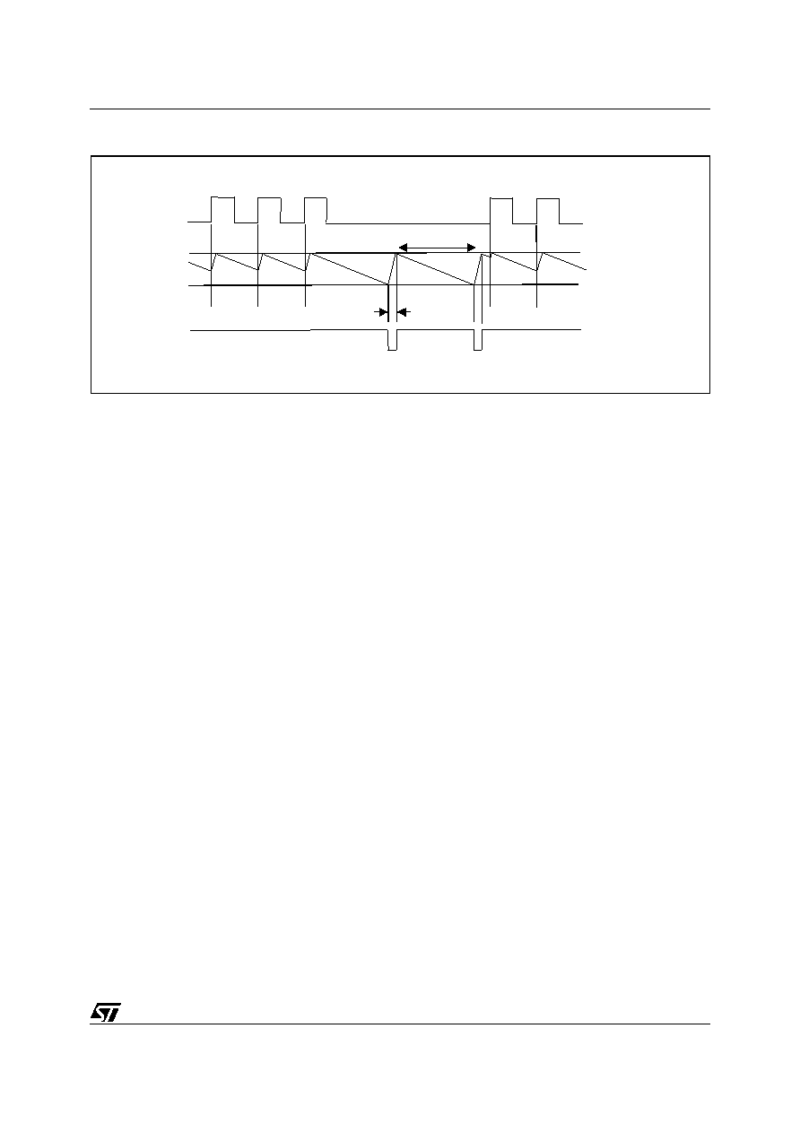
The reset circuit monitors the output voltage Vo. If the output voltage stays lower than Vo_th for filter time
trr, then Res goes low. If the output voltage Vo becomes lower than 2.0V (typ) than Res goes immediately
low. The reset low signal is guaranteed for an output voltage Vo greater than 1V.
When the output voltage goes back higher than Vo_th then Res goes high with a delay trd. This delay is
obtained by 512 period of an oscillator. The oscillator period is given by:
trd is given by
trd = 512 x Tosc
where:
Icr = 15
µ
A is an internally generated charge current,
Idr = 15
µ
A is an internally generated discharge current,
Vrhth=2.35V and Vrlth=0.65V are two typ thresholds,
Ctr is an external capacitance.
The Reset is always active and not depending on the state of WEn input pin.
Figure 2. Reset Time Diagram
Watchdog
The watchdog input Wi monitors a connected microcontroller. If pulses are missing, the Reset output
Res is set to low. The pulse sequence time can be set within a wide range with the external capacitor Ctw.
The watchdog circuit discharges the capacitor Ctw with the con-stant current Icwd. If the lower threshold
Vwlth is reached, a watchdog reset is generated.
To prevent this reset the microcontroller must generate a positive edge during the discharge of the capac-
itor before the voltage has reached the threshold Vwlth. In order to calculate the minimum time t
dis
during
which the microcontroller must output the positive edge the fol-lowing equation can be used
(Vwhth-Vwlth) x Ctw = Icwd x t
dis
Every Wi positive edge switches the current source from discharging to charging, the same happens when
the lower threshold is reached. When the voltage reaches the upper threshold Vwhth the current switches
from charging to discharging. The result is a saw toothwaveform at the watchdog timer capacitor Ctw.
The Watchdog operation is active only if WEn input pin is set to logic state high.
T
osc
V
rht h
V
rl th
≠
(
)
Ctr
Icr
-------------------------------------------------
V
rht h
V
rl th
≠
(
)
Ctr
Id
-------------------------------------------------
+
=
trr
< trr
trd = 512 Tosc
Tosc
Vrhth
Vrlth
Res
Vcr
Vo
Wi
Vout_th
trr
< trr
trd = 512 Tosc
Tosc
Vrhth
Vrlth
Res
Vcr
Vo
Wi
Vout_th
7/10
L4989
Figure 3. Watchdog time diagram
Res
Vcw
Wi
Vwlth
Vwhth
twol
Twop
Res
Vcw
Wi
Vwlth
Vwhth
twol
Twop

L4989
8/10
OUTLINE AND
MECHANICAL DATA
DIM.
mm
inch
MIN.
TYP.
MAX.
MIN.
TYP.
MAX.
A
1.35
1.75
0.053
0.069
A1
0.10
0.25
0.004
0.010
A2
1.10
1.65
0.043
0.065
B
0.33
0.51
0.013
0.020
C
0.19
0.25
0.007
0.010
D
(1)
4.80
5.00
0.189
0.197
E
3.80
4.00
0.15
0.157
e
1.27
0.050
H
5.80
6.20
0.228
0.244
h
0.25
0.50
0.010
0.020
L
0.40
1.27
0.016
0.050
k
0∞ (min.), 8∞ (max.)
ddd
0.10
0.004
Note:
(1) Dimensions D does not include mold flash, protru-
sions or gate burrs.
Mold flash, potrusions or gate burrs shall not exceed
0.15mm (.006inch) in total (both side).
SO-8
0016023 C
9/10
L4989
OUTLINE AND
MECHANICAL DATA
DIM.
mm
inch
MIN.
TYP.
MAX.
MIN.
TYP.
MAX.
A
2.35
2.65
0.093
0.104
A1
0.10
0.30
0.004
0.012
B
0.33
0.51
0.013
0.200
C
0.23
0.32
0.009
0.013
D
(1)
12.60
13.00
0.496
0.512
E
7.40
7.60
0.291
0.299
e
1.27
0.050
H
10.0
10.65
0.394
0.419
h
0.25
0.75
0.010
0.030
L
0.40
1.27
0.016
0.050
k
0∞ (min.), 8∞ (max.)
ddd
0.10
0.004
(1) "D" dimension does not include mold flash, protusions or gate
burrs. Mold flash, protusions or gate burrs shall not exceed
0.15mm per side.
SO20
0016022 D

Information furnished is believed to be accurate and reliable. However, STMicroelectronics assumes no responsibility for the consequences
of use of such information nor for any infringement of patents or other rights of third parties which may result from its use. No license is granted
by implication or otherwise under any patent or patent rights of STMicroelectronics. Specifications mentioned in this publication are subject
to change without notice. This publication supersedes and replaces all information previously supplied. STMicroelectronics products are not
authorized for use as critical components in life support devices or systems without express written approval of STMicroelectronics.
The ST logo is a registered trademark of STMicroelectronics.
All other names are the property of their respective owners
© 2004 STMicroelectronics - All rights reserved
STMicroelectronics GROUP OF COMPANIES
Australia - Belgium - Brazil - Canada - China - Czech Republic - Finland - France - Germany - Hong Kong - India - Israel - Italy - Japan -
Malaysia - Malta - Morocco - Singapore - Spain - Sweden - Switzerland - United Kingdom - United States
www.st.com
10/10
L4989