1/4
L603 - L604
September 2003
s
EIGHT DARLINGTONS PER PACKAGE
s
OUTPUT CURRENT 400 mA PER DRIVER
(500mA PEAK)
s
OUTPUT VOLTAGE 90 V (V
CE (sus)
) = 70 V)
s
INTEGRAL SUPPRESSION DIODES FOR
INDUCTIVE LOADS
s
OUTPUTS CAN BE PARALLELED FOR
HIGHER CURRENT
s
TTL / CMOS INPUTS
s
INPUTS PINNED OPPOSITE OUTPUTS TO
SIMPLIFY LAYOUT
DESCRIPTION
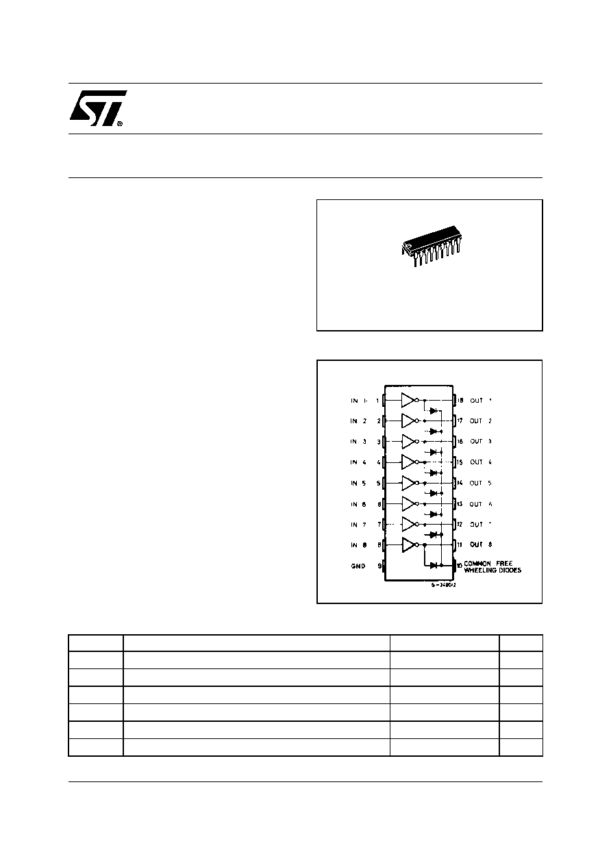
The L603 and L604 are high voltage, high current
darlington arrays each containing eight open col-
lector darlington pairs with common emitters. Each
channel is rated at 400mA and can with stand
peak currents of 500 mA.
Suppression diodes are included for inductive load
driving and the inputs are pinned opposite the out-
puts to simplify board layout.
The four versions interface to all common logic
families:
L603 = 5V TTL
L604 = 6 - 15V CMOS
These versatile devices are useful for driving a
wide range of loads, including solenoids, relays
DC motors, LED displays, filament lamps, thermal
printheads and high power buffers.
PIN CONNECTION (top view)
DIP18
ORDERING NUMBERS: L603C L604C
DARLINGTON ARRAYS
ABSOLUTE MAXIMUM RATINGS
Symbol
Parameter
Value
Unit
V
CEX
Collector Emitter Voltage (input open)
90
V
I
C
Collector Current
0.4
A
I
C
Collector Peak Current
0.5
A
V
i
Input Voltage (for L603 and L604)
30
V
P
tot
Total Power Dissipation a T
amb
= 25∞C
1.8
W
T
op
Operating Junction Temperature
-25 to 150
∞
C
L603 - L604
2/4
THERMAL DATA
ELECTRICAL CHARACTERISTCS
Symbol
Parameter
Value
Unit
R
th-j amb
Thermal Resistance Junction ambient
max 70
∞C/W
Symbol
Parameter
Test Condition
Min.
Typ.
Max.
Unit
I
CEX
Output Leakage Current
V
CE
= 90V
10
µ
A
V
CE(sat)
Collector Emitter Saturation
Voltage
I
C
= 300mA; I
B
= 500
µ
A
2
V
I
C
= 200mA; I
B
=
µ
A
1.7
V
I
C
= 100mA; I
B
= 250
µ
A
1.2
V
V
i
Maximum Input Voltage
(ON condition)
V
CE
= 3V; I
C
= 300mA
L603
L604
2.5
5
V
V
V
i
Maximum Input Voltage
(OFF condition)
V
CE
= 90V; I
C
= 25
µ
A
L603
L604
0.75
1
V
V
I
R
Clamp Diode Reverse Current
V
R
= 90V
50
µ
A
V
F
Clamp Diode Forward Voltage
I
F
= 300mA
2
2.4
V
t
on
Turn-on Delay
0.5 V
i
to 0.5 V
o
0.4
µ
s
t
off
Turn-off Delay
0.5 V
i
to 0.5 V
o
0.4
µ
A
L603
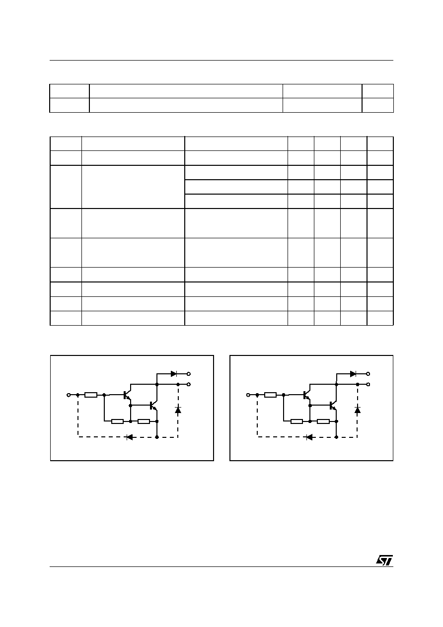
L604
2.7K
IN
COM
OUT
EACH DRIVER
7.2K
3K
D03IN1490
10.5K
IN
COM
OUT
EACH DRIVER
7.2K
3K
D03IN1491

Information furnished is believed to be accurate and reliable. However, STMicroelectronics assumes no responsibility for the consequences
of use of such information nor for any infringement of patents or other rights of third parties which may result from its use. No license is granted
by implication or otherwise under any patent or patent rights of STMicroelectronics. Specifications mentioned in this publication are subject
to change without notice. This publication supersedes and replaces all information previously supplied. STMicroelectronics products are not
authorized for use as critical components in life support devices or systems without express written approval of STMicroelectronics.
The ST logo is a registered trademark of STMicroelectronics.
All other names are the property of their respective owners
© 2003 STMicroelectronics - All rights reserved
STMicroelectronics GROUP OF COMPANIES
Australia - Belgium - Brazil - Canada - China - Czech Republic - Finland - France - Germany - Hong Kong - India - Israel - Italy - Japan -
Malaysia - Malta - Morocco - Singapore - Spain - Sweden - Switzerland - United Kingdom - United States
www.st.com
4/4
L603 - L604