L6114
L6115
April 1993
QUAD 100 V, DMOS SWITCH
.
OUTPUT VOLTAGE TO 100 V
.
0.7
R
DS(ON)
.
SUPPLY VOLTAGE UP TO 60 V
.
LOW INPUT CURRENT
.
TTL/CMOS COMPATIBLE INPUTS
.
HIGH SWITCHING FREQUENCY (200 KHz)
DESCRIPTION
Realized with the Multipower-BCD mixed bipo-
lar/CMOS/DMOS process, the L6114/15 monolithic
quad DMOS switch is designed for high current,
high voltage switching applications. Each of the four
switches is controlled by a logic input and all four are
controlled by a common enable input. All inputs are
TTL/CMOS compatible for direct connection to logic
circuits. Each source is available for the insertion of
the sense resistors in current control applications.
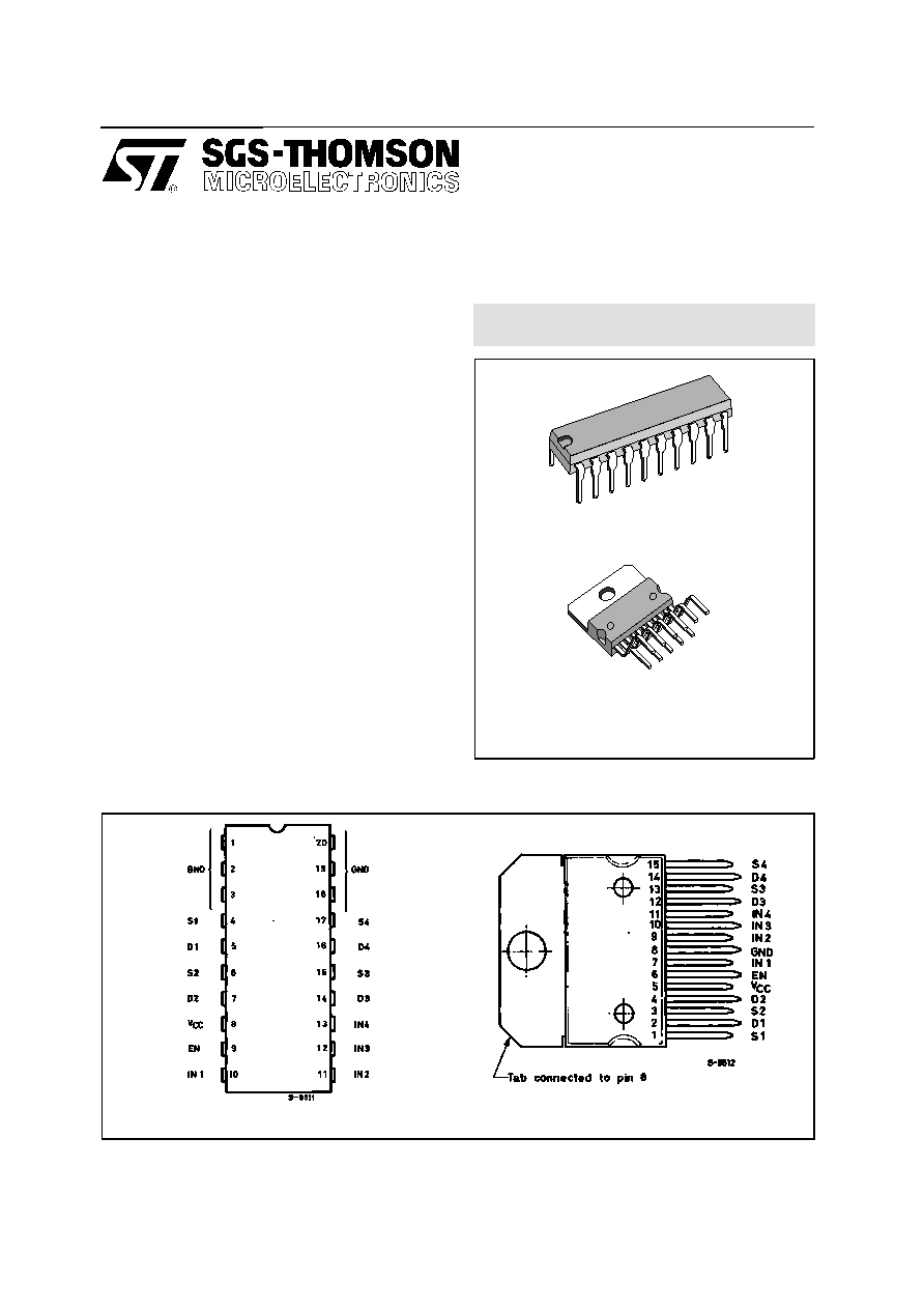
Two versions are available : the L6114 mounted in
a Powerdip 14+3+3 package and the L6115 in a 15-
lead Multiwatt package.
ORDERING NUMBERS : L6114 (Powerdip)
L6115 (Multiwatt-15)
Multiwatt-15
PIN CONNECTIONS (top view)
Powerdip 14 + 3 + 3
L6115 (Multiwatt-15)
L6114 (Powerdip)
MULTIPOWER BCD TECHNOLOGY
1/11
ABSOLUTE MAXIMUM RATINGS
Symbol
Parameter
Value
Unit
V
DS
Drain-source Voltage
100
V
V
CC
Supply Voltage
60
V
I
D
Continuous Drain Current
@<0>T
pins
= 90
�
C
@<0>T
case
= 90
�
C
Powerdip
Multiwatt �15
1.5
3
A
A
I
DM
(*)
Pulsed Drain Current
Powerdip
Multiwatt �15
5
8
A
A
I
SD
Continuous Source-drain
Diode Current
@<0>T
pins
= 90
�
C
@<0>T
case
= 90
�
C
Powerdip
Multiwatt �15
1.5
3
A
A
I
SDM
Pulsed Source Drain Diode Current
Powerdip
Multiwatt �15
5
8
A
A
V
IN
Input Voltage
7
V
V
EN
Enable Voltage
7
V
V
S
Source Voltage
� 1 to + 4
V
P
tot
Total Power Dissipation
@ T
pins
= 90
�
C
@ T
case
= 90
�
C
@ T
amb
= 70
�
C
@ T
amb
= 70
�
C
Powerdip
Multiwatt �15
Powerdip
Multiwatt �15
4.3
20
1.3
2.3
W
W
W
W
T
stg
, T
j
Storage and Junction Temperature Range
� 40 to + 150
�
C
(*) Pulse width
300
�
s, duty cycle
10 %.
Note : I
D
, I
DM
, I
SD
, I
SDM
are given per channel.
THERMAL DATA
Symbol
Parameter
Powerdip
Multiwatt�15
Unit
R
th j-pins
Thermal Resistance Junction-pins
Max.
14
-
o
C/W
R
th j-case
Thermal Resistance Junction-case
Max.
-
3
o
C/W
R
th j-amb
Thermal Resistance Junction-ambient
Max.
65
35
o
C/W
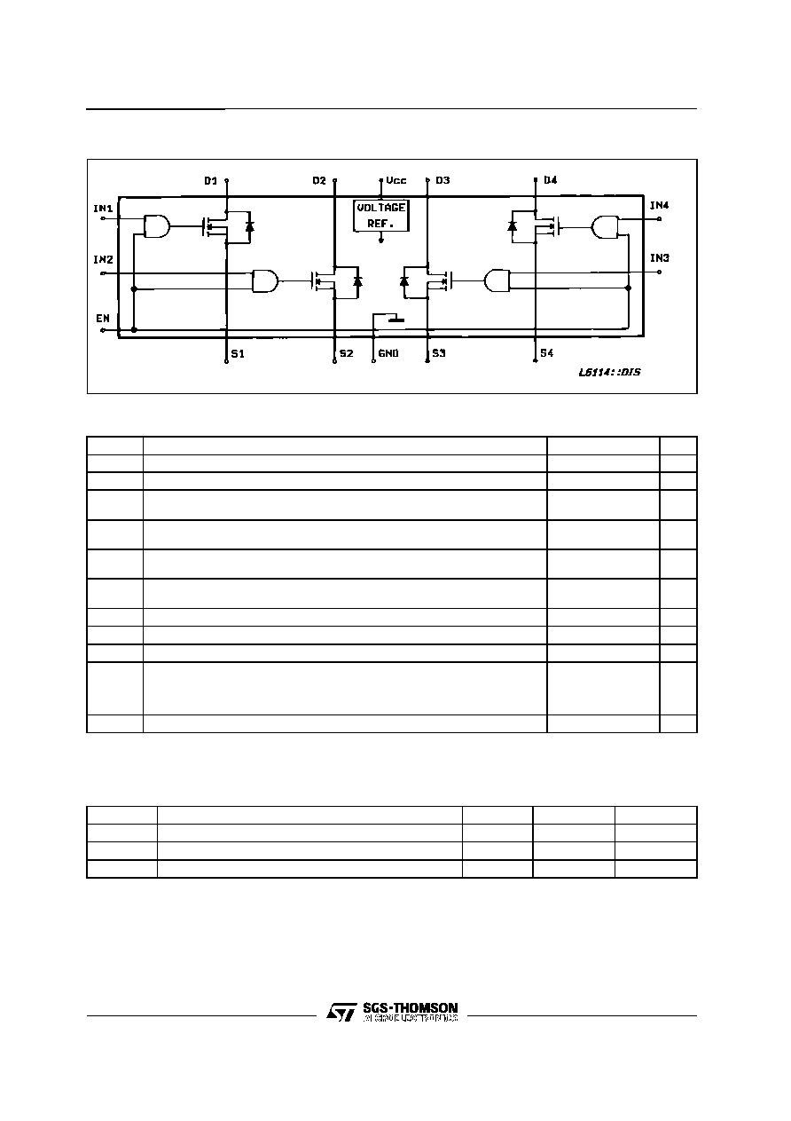
BLOCK DIAGRAM
L6114 - L6115
2/11

ELECTRICAL CHARACTERISTICS (T
j
= 25
o
C, V
CC
= 40V, unless otherwise specified)
Symbol
Parameter
Test Conditions
Min.
Typ.
Max.
Unit
V
CC
Supply Voltage
14
48
V
I
CC
Supply Current
All V
IN
= H
V
EN
= Square Wave
(200kHz, 50 % DC)
9
mA
I
Q
Quiescent Current
V
EN
= L
2
3
mA
BV
DSS
Drain Source Breakdown Voltage
I
D
= 1mA, V
EN
= L
100
V
I
DSS
Output Leakage Current
V
EN
= L
V
DS
= 100V
V
DS
= 80V, T
j
= 125
�
C
1
1
mA
R
DS (on)
(*)
Static Drain-source on Resistance
V
CC
14V, I
D
= 1.5A
V
EN
, V
IN
= H
0.7
V
IN L
, V
EN L
Input Low Voltage
� 0.3
0.8
V
V
IN H
, V
EN H
Input High Voltage
2
7
V
I
IN L
, I
EN L
Input Low Current
V
IN
, V
EN
= L
� 100
�
A
I
IN H
, I
EN H
Input High Current
V
IN
, V
EN
= H
10
�
A
t
d (on)
Turn on Delay Time
I
D
= 1.5A
See Test Circuit and
Waveforms
300
ns
t
r
Rise Time
100
ns
t
d (off)
Turn off Delay Time
400
ns
t
f
Fall Time
100
ns
V
SD
(*)
Source Drain Diode Forward Voltage
I
SD
= 1.5A, V
EN
= L
1.5
V
V
SD (on)
(*)
Source Drain Forward Voltage
I
SD
= 1.5A - V
IN
, V
EN
= H
1.2
V
(*) Pulse test : pulse width = 300
�
s, duty cycle = 2 %.
L6114 - L6115
3/11

SWITCHING TIMES RESISTIVE LOAD
Figure 1 : Test Circuit
(Pins x = Powerdip ; Pins (x) = Multiwatt).
Figure 2 : Waveforms.
b)
a)
L6114 - L6115
4/11

TEST CIRCUIT (Pins x = Powerdip ; Pins (x) = Multiwatt)
Figure 3 : Quiescent Current and Output
Leakage Current..
Figure 4 : Supply Current.
Figure 5 : R
DS (on)
.
Figure 6 : Source-drain Diode Forward Voltage.
V
CC
= 14 V,
V
IN
= 2 V,
V
EN
= 2V
I
D
= square wave,
f = 3 KHz
DC = 2 %
(*) V
DS
is taken during the time in which the
V
DS
I
D
= 1.5 A
R
DS
=
1.5
V
IN
= 2 V,
I
SD
square wave, f = 3 KHz
DC = 2 %
-
Set V
EN
= 0.8 V for V
SD
(taken during the time in which
I
SD
= 1.5 A)
-
Set V
EN
= 2 V for V
SD
(on)
(taken during the time in which
I
SD
= 1.5 A)
V
EN
= 0.8 V
V
IN
= 2 V
V
EN
= square wave
{
f = 200 KHz
DC = 50 %
L6114 - L6115
5/11