 | –≠–ª–µ–∫—Ç—Ä–æ–Ω–Ω—ã–π –∫–æ–º–ø–æ–Ω–µ–Ω—Ç: L6220N | –°–∫–∞—á–∞—Ç—å:  PDF PDF  ZIP ZIP |
L6220
L6220N
April 1993
QUAD DARLINGTON SWITCHES
.
TWO NON INVERTING + TWO INVERTING IN-
PUTS WITH INHIBIT
.
OUTPUT VOLTAGE UP TO 50V
.
OUTPUT CURRENT UP TO 1.8A
.
VERY LOW SATURATION VOLTAGE
.
TTL COMPATIBLE INPUTS
.
INTEGRAL FAST RECIRCULATION DIODES
DESCRIPTION
The L6220 monolithic quad darlington switch is de-
signed for high current, high voltage switching appli-
cations. Each of the four switches is controlled by a
logic input and all four are controlled by a common
inhibit input. All inputs are TTL-compatible for direct
connection to logic circuits.
Each switch consists of an open-collector darlington
transistor plus a fast diode for switching applications
with inductive loads. The emitters of the four
switches are commoned. Any number of inputs and
outputs of the same device may be paralleled.
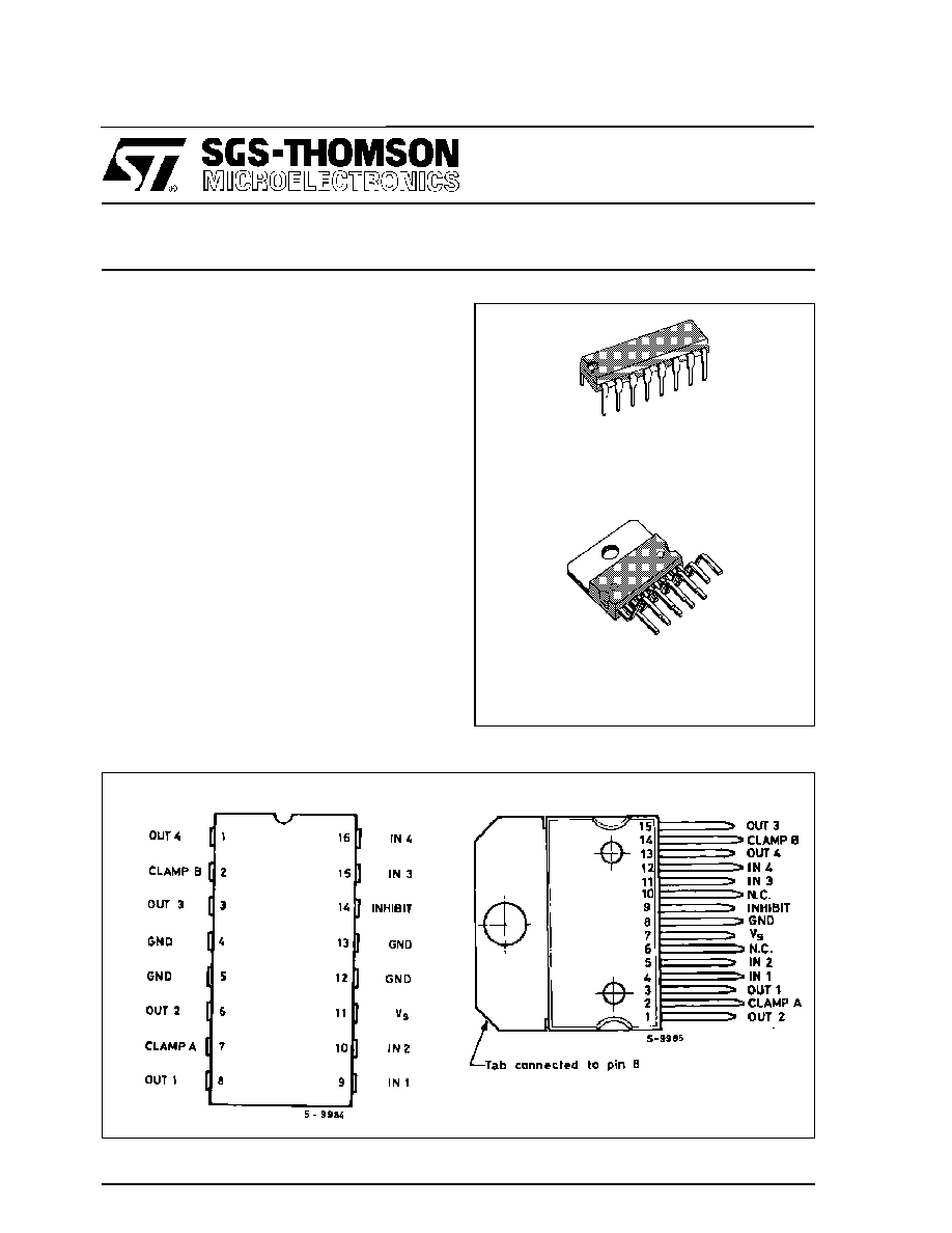
Two versions are available : the L6220 mounted in
a Powerdip 12 + 2 + 2 package and the L6220N
mounted in a 15-lead Multiwatt package.
Multiwatt 15
(Plastic Package)
ORDERING NUMBER : L6220N
Powerdip 12 + 2 + 2
(Plastic Package)
ORDERING NUMBER : L6220
PIN CONNECTIONS (top views)
L6220 (Powerdip)
L6220N (Multiwatt-15)
1/12
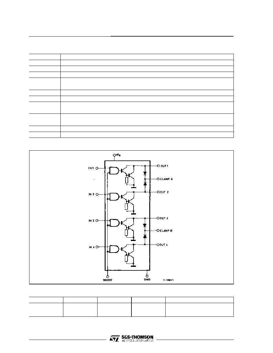
BLOCK DIAGRAM
PIN FUNCTIONS (see block diagram)
Name
Function
IN 1
Input to Driver 1
IN 2
Input to Driver 2
OUT 1
Output of Driver 1
OUT 2
Output of Driver 2
CLAMP A
Diode Clamp to Driver 1 and Driver 2
IN 3
Input to Driver 3
IN 4
Input to Driver 4
OUT 3
Output of Driver 3
OUT 4
Output of Driver 4
CLAMP B
Diode Clamp to Driver 3 and Driver 4
INHIBIT
Inhibit Input to all Drivers
V
s
Logic Supply Voltage
GND
Common Ground
For each input : H = High level
L = Low level
TRUTH TABLE
Inhibit
Input 1, 4
Power Out
Inhibit
Inputs 2, 3
Power Out
L
L
H
H
L
X
ON
OFF
OFF
L
L
H
L
H
X
ON
OFF
OFF
L6220 - L6220N
2/12

THERMAL DATA
Symbol
Parameter
Powerdip
Multiwatt≠15
Unit
R
th j-pins
Thermal Resistance Junction-pins
Max.
14
-
o
C/W
R
th j-case
Thermal Resistance Junction-case
Max.
-
3
o
C/W
R
th j-amb
Thermal Resistance Junction-ambient
Max.
80
35
o
C/W
ABSOLUTE MAXIMUM RATINGS
Symbol
Parameter
Value
Unit
V
o
Ouput Voltage
50
V
V
s
Logic Supply Voltage
7
V
V
IN
, V
INH
Input Voltage, Inhibit Voltage
V
s
I
C
Continuous Collector Current (for each channel)
1.8
A
I
C
Collector Peak Current (repetitive, duty cycle = 10 % t
on
= 5 ms)
2.5
A
I
C
Collector Peak Current (non repetitive, t = 10
µ
s)
3.2
A
T
op
Operating Temperature Range (junction)
≠ 40 to + 150
∞
C
T
stg
Storage Temperature Range
≠ 55 to + 150
∞
C
I
su b
Output Substrate Current
350
mA
P
tot
Total Power Dissipation
at T
pins
=
90
o
C (Powerdip)
at T
case
=
90
o
C (Multiwatt)
at T
amb
=
70
o
C (Powerdip)
at T
amb
=
70
o
C (Multiwatt)
4.3
20
1
2.3
W
W
W
W
ELECTRICAL CHARACTERISTICS
Refer to the test circuits Fig. 1 to Fig.9 (V
S
= 5V, T
amb
= 25
o
C unless otherwise specified)
Symbol
Parameter
Test Conditions
Min.
Typ.
Max.
Unit
V
S
Logic Supply Voltage
4.5
5.5
V
I
s
Logic Supply Current
All Outputs ON, I
C
= 0.7A
All Outputs OFF
20
20
mA
MA
V
CE (sus)
Output Sustaining Voltage
I
C
=100mA, V
INH
= V
INH
H
46
V
I
CEX
Output Leakage Current
V
CE
= 50V, V
IN 1.4
= V
INH
H
1
mA
V
CE (sat )
Collector Emitter Saturation Voltage
(one output on ; all others off.)
V
s
= 4.5V, V
IN 2.3
= V
IN
L
V
INH
= V
INH
L
I
C
= 0.6A
I
C
= 1A
I
C
= 1.8A
1
1.2
1.6
V
V
IN
L,
V
INH
L
Input Low Voltage
0.8
V
I
IN
L, I
INH
L
Input Low Current
V
IN
= V
IN
L, V
INH
= V
INH
L
- 100
µ
A
V
IN
H,
V
INH
H
Input High Voltage
2.0
V
I
IN
H, I
INH
H
Input High Current
V
IN
= V
IN
H, V
INH
= V
INH
H
±
10
µ
A
I
R
Clamp Diode Leakage Current
V
R
= 50V, V
INH
= V
INH
H
100
µ
A
V
F
Clamp Diode Forward Voltage
I
F
= 1A
I
F
= 1.8A
1.6
2.0
V
V
t
d (on)
Turn on Delay Time
V
p
= 5V, R
L
= 10
2
µ
s
t
d (off)
Turn off Delay Time
V
p
= 5V, R
L
= 10
5
µ
s
I
s
Logic Supply Current Variation
V
IN
= 5V, V
EN
= 5V
I
out
= ≠ 300mA for each Channel
120
mA
L6220 - L6220N
3/12
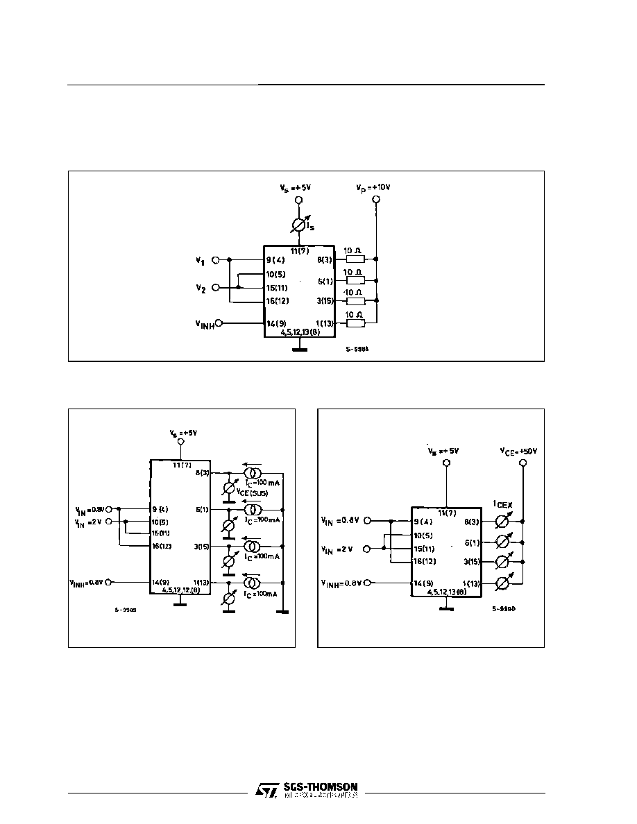
TEST CIRCUITS
(X) = Referred to Multiwatt package
X = Referred to Powerdip package
Figure 1 : Logic Supply Current.
Set V
1
= 4.5V, V
2
= 0.8V, V
INH
= 4.5V or V
1
= 0.8V, V
2
= 4.5V, V
INH
= 0.8 for I
S
(all outputs off).
Set V
1
= 2V, V
2
= 0.8V, V
INH
= 0.8V for I
S
(all outputs on).
Figure 2 : Output Sustaining Voltage.
Figure 3 : Output Leakage Current.
L6220 - L6220N
4/12
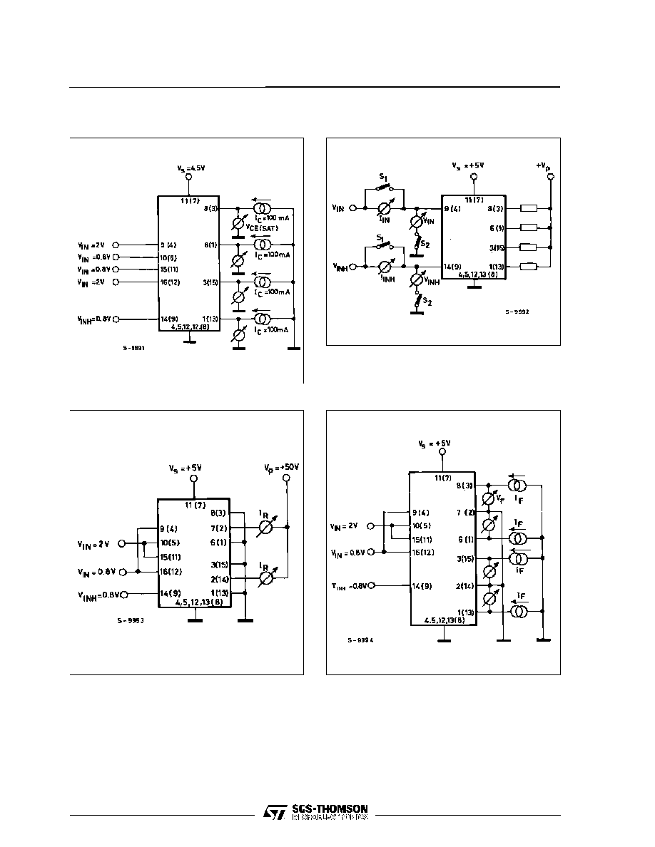
Figure 4 : Collector-emitter Saturation
Figure 5 : Logic Input Characteristics.
Set S
1
, S
2
open, V
IN
, V
INH
= 0.8V for I
IN
L, I
INH
L
Set S
1
, S
2
open, V
IN
, V
INH
= 2V for I
IN
H, I
INH
H
Set S
1
, S
2
close, V
IN
, V
INH
= 0.8V for V
IN
L, V
INH
L
Set S
1
, S
2
close, V
IN
, V
INH
= 2V for V
IN
H, V
INH
H.
Figure 6 : Clamp Diode Leakage Current.
Figure 7 : Clamp Diode Forward Voltage.
L6220 - L6220N
5/12
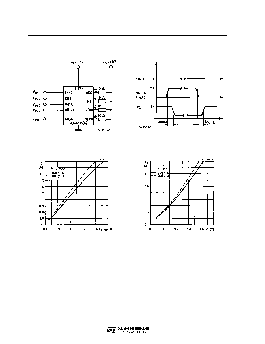
Figure 8 : Switching Times Test Circuit.
Figure 9 : Switching Times Waveforms.
Figure 10 : Collector Saturation Voltage versus
Collector Current
Figure 11 : Free- wheeling Diode ForwardVoltage
versus Diode Current
L6220 - L6220N
6/12
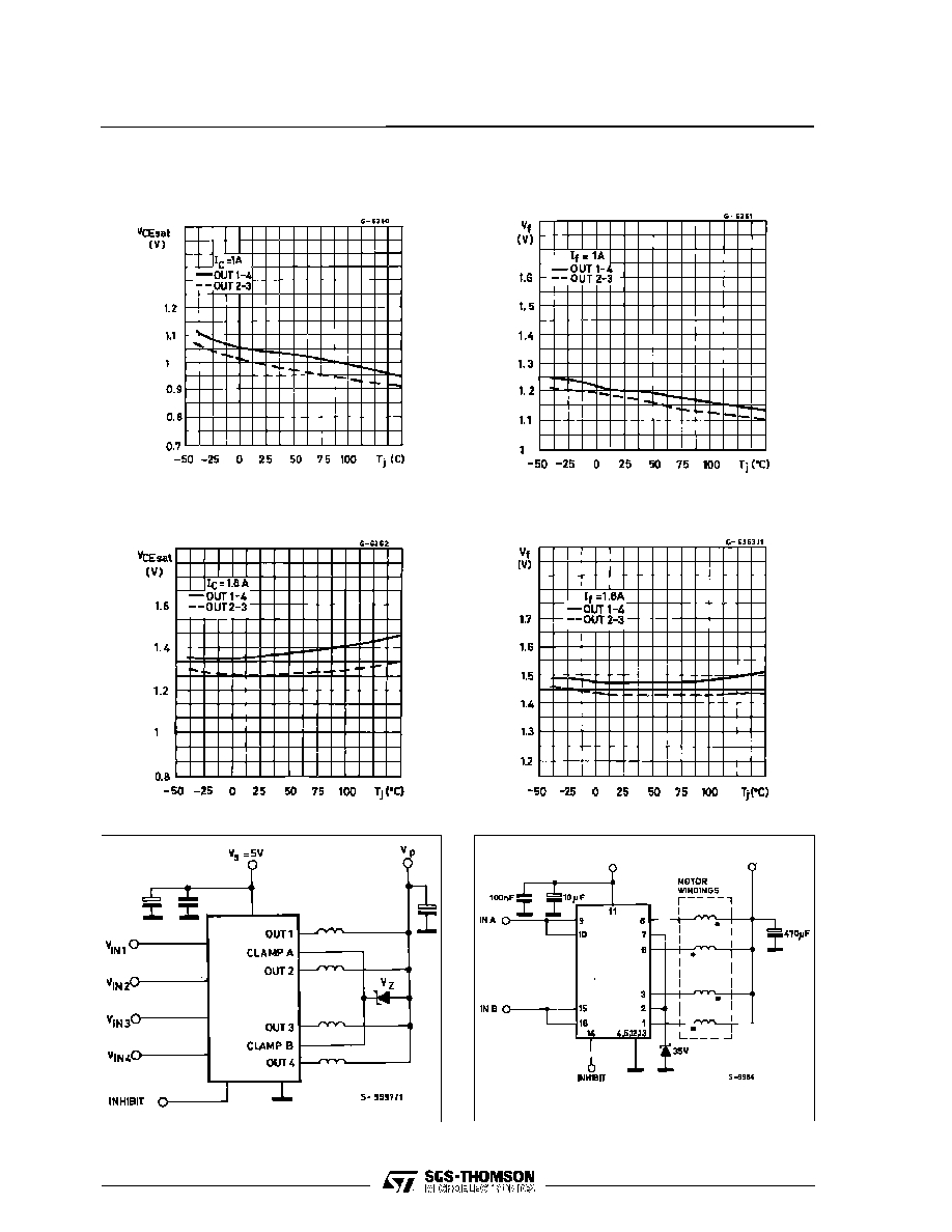
Figure 14 : Collector Saturation Voltage versus
Junction Temperature at IC = 1.8A
Figure 15 : Free-wheeling Diode Forward Volt-
age versus Junction Temperature
at I
F
= 1.8A
Figure 16.
Figure 17 : Unipolar Stepper Motor Driver.
Figure 12 : Collector Saturation Voltage versus
Junction Temperature at IC = 1A
Figure 13 : Free-wheeling Diode Forward Voltage
versus Junction Temperature
at If = 1A
L6220 - L6220N
7/12
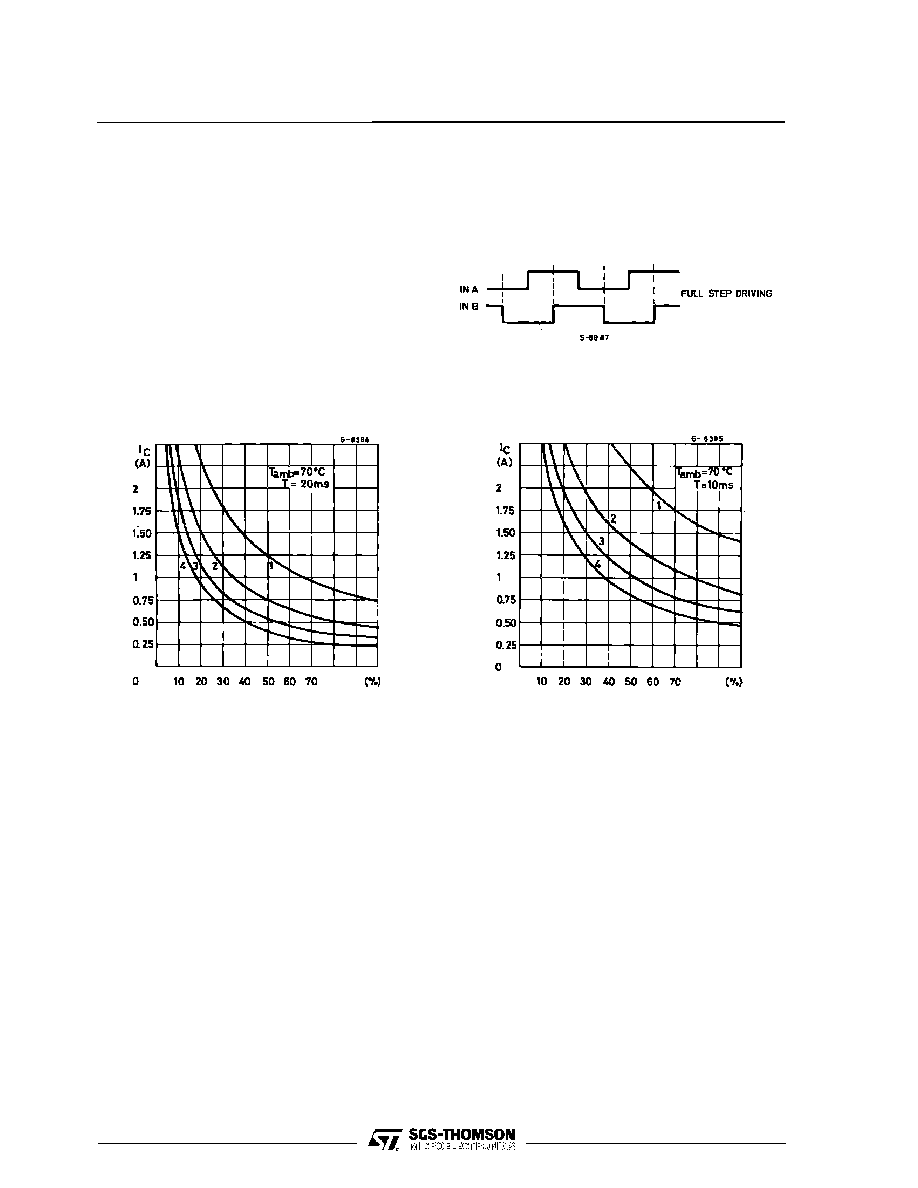
Figure 18 : Allowed Peak Collector-current versus
Duty Cycle for 1, 2, 3 or 4 Contempo-
rary Working Outputs (L6220).
Figure 19 : Allowed Peak Collector Cur-rent ver-
sus Duty Cycle for 1, 2, 3 or 4 Con-
temporary Working Outputs
(L6220N).
APPLICATION INFORMATION
When inductive loads are driven by L6220/N, a
zener diode in series with the integral free-wheeling
diodes increases the voltage across which energy
stored in the load is discharged and therefore
speeds the current decay (Fig. 16). For reliability it
is suggested that the zener is chosen so that V
p
+
V
z
< 35 V.
The reasons for this are two fold :
1) The zener voltage changes in temperature and
current.
2) The instantaneouspower must be limited to
avoid the reverse second breakdown.
The particular internal logic allows an easier full step
driving using only two input signals.
MOUNTING INSTRUCTION
The R
th j-amb
of the L6220 can be reduced by solder-
ing the GND pins to a suitable copper area of the
printed circuit board (Fig. 20) or to an external
heatsink (Fig. 21).
The diagram of figure 22 shows the maximum dis-
sipable power P
tot
and the R
th j-amb
as a function of
the side "
" of two equal square copper areas hav-
ing a thickness of 35
µ
(1.4 mils). During soldering
the pins temperature must not exceed 260
∞
C and
the soldering time must not be longer than 12 sec-
onds.
The external heatsink or printed circuit copper area
must be connected to electrical ground.
L6220 - L6220N
8/12
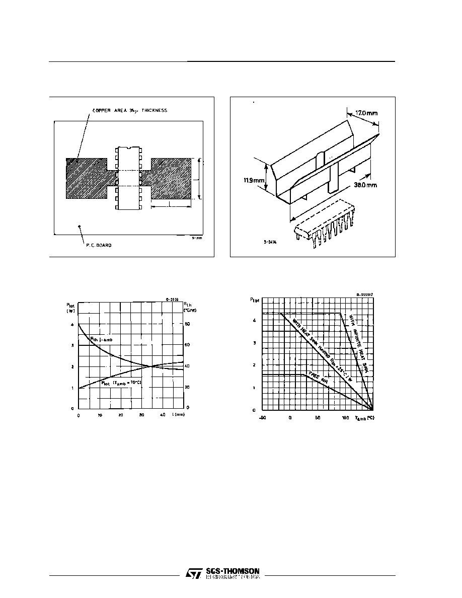
Figure 22 : Maximum Dissipable Power and Junc-
tion to Ambient Thermal Resistance
versus Side "
"
Figure 23 : Maximum Allowable Power Dissipa-
tion versus Ambient Temperature
Figure 20 : Example of P.C. Board Copperarea
which is used as Heatsink
Figure 21 : External Heatsink Mounting Example
L6220 - L6220N
9/12
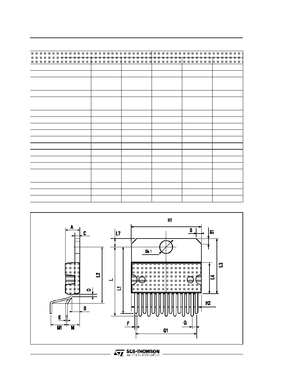
MULTIWATT15 PACKAGE MECHANICAL DATA
DIM.
mm
inch
MIN.
TYP.
MAX.
MIN.
TYP.
MAX.
A
5
0.197
B
2.65
0.104
C
1.6
0.063
D
1
0.039
E
0.49
0.55
0.019
0.022
F
0.66
0.75
0.026
0.030
G
1.14
1.27
1.4
0.045
0.050
0.055
G1
17.57
17.78
17.91
0.692
0.700
0.705
H1
19.6
0.772
H2
20.2
0.795
L
22.1
22.6
0.870
0.890
L1
22
22.5
0.866
0.886
L2
17.65
18.1
0.695
0.713
L3
17.25
17.5
17.75
0.679
0.689
0.699
L4
10.3
10.7
10.9
0.406
0.421
0.429
L7
2.65
2.9
0.104
0.114
M
4.2
4.3
4.6
0.165
0.169
0.181
M1
4.5
5.08
5.3
0.177
0.200
0.209
S
1.9
2.6
0.075
0.102
S1
1.9
2.6
0.075
0.102
Dia1
3.65
3.85
0.144
0.152
L6220 - L6220N
10/12
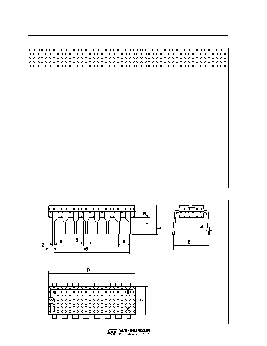
POWERDIP16 PACKAGE MECHANICAL DATA
DIM.
mm
inch
MIN.
TYP.
MAX.
MIN.
TYP.
MAX.
a1
0.51
0.020
B
0.85
1.40
0.033
0.055
b
0.50
0.020
b1
0.38
0.50
0.015
0.020
D
20.0
0.787
E
8.80
0.346
e
2.54
0.100
e3
17.78
0.700
F
7.10
0.280
I
5.10
0.201
L
3.30
0.130
Z
1.27
0.050
L6220 - L6220N
11/12

Information furnished is believed to be accurate and reliable. However, SGS-THOMSON Microelectronics assumes no responsibility for
the consequences of use of such information nor for any infringement of patents or other rights of third parties which may result from its
use. No license is granted by implication or otherwise under any patent or patent rights of SGS-THOMSON Microelectronics. Specifica-
tions mentioned in this publication are subject to change without notice. This publication supersedes and replaces all information pre-
viously supplied. SGS-THOMSON Microelectronics products are not authorized for use as critical components in life support devices or
systems without express written approval of SGS-THOMSON Microelectronics.
©
1994 SGS-THOMSON Microelectronics - All Rights Reserved
MULTIWATT
Æ
is a Registered Trademark
SGS-THOMSON Microelectronics GROUP OF COMPANIES
Australia - Brazil - France - Germany - Hong Kong - Italy - Japan - Korea - Malaysia - Malta - Morocco - The Netherlands - Singapore -
Spain - Sweden - Switzerland - Taiwan - Thaliand - United Kingdom - U.S.A.
L6220 - L6220N
12/12