 | –≠–ª–µ–∫—Ç—Ä–æ–Ω–Ω—ã–π –∫–æ–º–ø–æ–Ω–µ–Ω—Ç: L6225 | –°–∫–∞—á–∞—Ç—å:  PDF PDF  ZIP ZIP |

1/10
L6225
March 2001
This is preliminary information on a new product now in development or undergoing evaluation. Details are subject to change with out notice.
s
OPERATING SUPPLY VOLTAGE FROM 8 TO
52V
s
2.8A PEAK CURRENT (1.4A DC)
s
R
DS (ON)
0.73
TYP. VALUE @ T
j
= 25
∞
C
s
CROSS CONDUCTION PROTECTION
s
THERMAL SHUTDOWN
s
OPERATING FREQUENCY UP TO 100KHz
s
HIGH SIDE OVER CURRENT PROTECTION
s
CMOS/TTL INPUT
s
INTRINSIC FAST FREE WHEELING DIODES
s
UNDER VOLTAGE LOCKOUT
TYPICAL APPLICATIONS
s
STEPPER MOTOR
s
DUAL OR QUAD DC MOTOR
DESCRIPTION
The L6225 is a dual full bridge driver for motor control
applications manufactured with Multipower BCD
technology which combines isolated DMOS power
transistors with CMOS and bipolar circuits on the
same chip.
The Logic Inputs are CMOS/TTL and
µ
P compatible.
The High Side switches are protected against unsafe
over current conditions.
Each full bridge is controlled by a separate Enable
and has a sense pin for the current sense resistor in-
sertion. Another feature is the thermal shutdown.
The L6225 is assembled in PowerDIP20(16+2+2),
PowerSO20 and SO20(16+2+2) packages.
PowerDIP20
PowerSO20
SO20
(16+2+2)
(16+2+2)
ORDERING NUMBERS:
L6225N
L6225PD
L6225D
PRELIMINARY DATA
DUAL DMOS FULL BRIDGE MOTOR DRIVER
BLOCK DIAGRAM
IN1
B
GND
GND
V
S A
V
S A
V
S A
Logic
&
Drivers
V
S B
V
S B
V
S B
Charg e
Pump
GND
V
S A
OUT2
A
V
CP
EN
B
IN1
A
IN2
A
SENSE
A
OUT1
A
GND
V
S B
OUT2
B
V
BO OT
EN
A
IN2
B
SENSE
B
OUT1
B
L6225
2/10
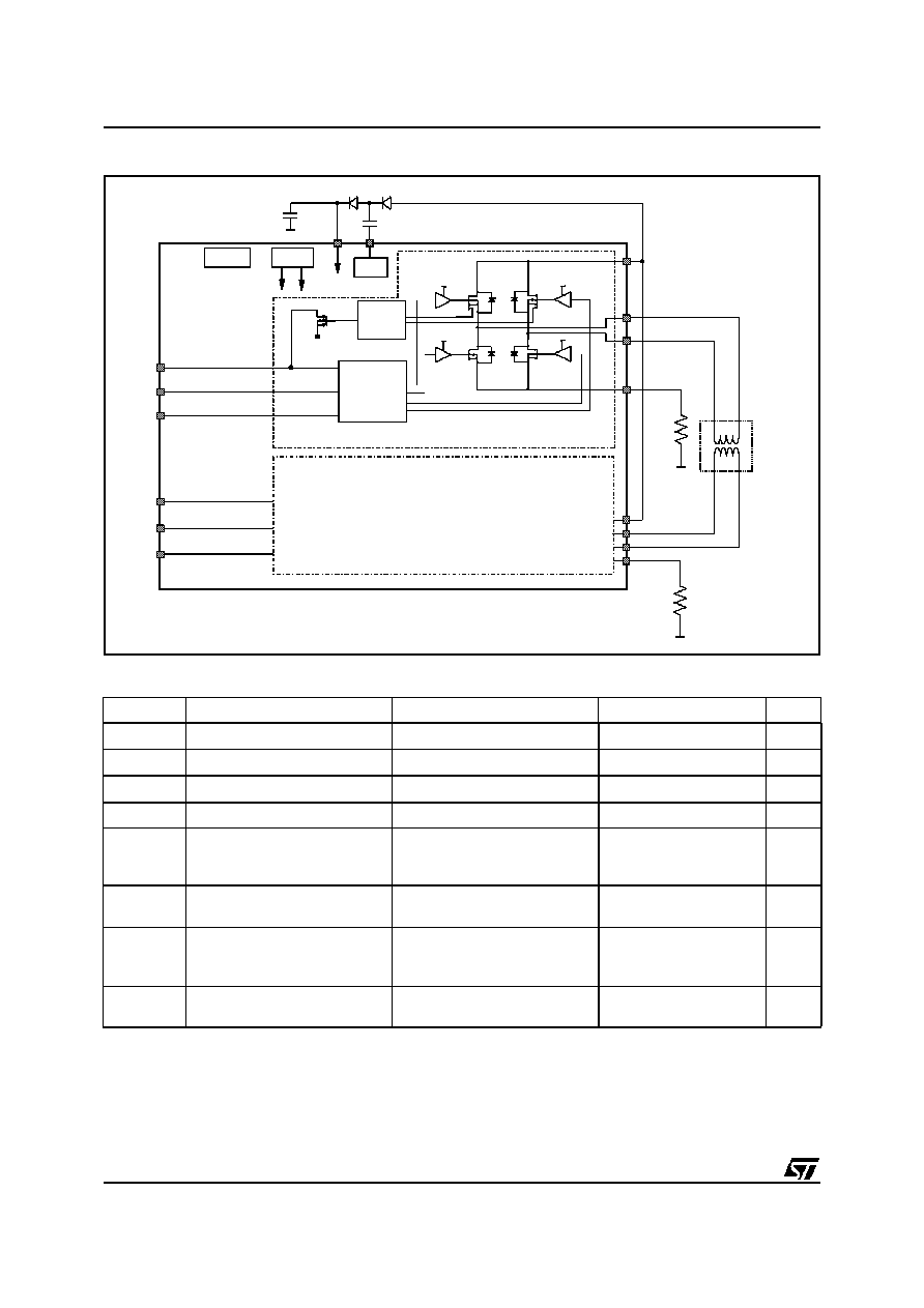
FUNCTIONAL BLOCK DIAGRAM
ABSOLUTE MAXIMUM RATINGS
Symbol
Parameter
Test conditio ns
Value
Unit
V
S
Supply Voltage
60
V
V
IN
,V
EN
Input and Enable Voltage Range
-0.3 to +7
V
V
SENSE
DC Sensing Voltage Range
-1 to +4
V
V
BOOT
Bootstrap Peak Voltage
V
S
+ 10
V
I
S(peak)
Pulsed Supply Current (for each
V
S
pin), internally limited by the
overcurrent protection
t
PULSE
< 1ms
3.55
A
I
S
DC Supply Current (for each V
S
pin)
1.4
A
V
OD
Differential Voltage Between
V
S A
, OUT1
A
, OUT2
A
, SENSE
A
and
V
S B
, OUT1
B
, OUT2
B
, SENSE
B
60
V
T
stg
, T
OP
Storage and Operating
Temperature Range
-40 to 150
∞
C
IN2
A
Vboot
10V
Vboot
10V
Voltage
Regulator
10V
5V
Thermal
Protection
BRIDGE A
EN
A
IN1
A
SENSE
V
OUT1
OUT2
SENSE
V
OUT1
OUT2
Charge
Pump
Vboot
EN
B
IN1
B
IN2
B
Logic
Vboot
VCP
BRIDGE B
Over
Current
Detection
BIPOLAR
STEPPER
MOTOR
SA
A
A
A
SB
B
B
B
3/10
L6225
RECOMMENDED OPERATING CONDITIONS
PIN CONNECTION (Top View)
Symbol
Parameter
MIN
MAX
Unit
V
S
Supply Voltage
12
52
V
V
OD
Differential Voltage Between
V
S A
, OUT1
A
, OUT2
A
, SENSE
A
and
V
S B
, OUT1
B
, OUT2
B
, SENSE
B
52
V
V
SENSE
Sensing voltage
(pulsed tw<t
rr
)
(DC)
-6
-1
6
1
V
V
V
ref
V
ref
Operating Voltage
-0.1
5
V
I
OUT
DC Output Current
1.4
A
T
j
Operating Junction Temperature
-25
+125
∞
C
f
sw
Switching Frequency
100
kHz
PowerDIP20/SO20
GND
OUT1A
SENSEA
IN2A
IN1A
VCP
ENA
OUT2A
VSA
VSB
OUT2B
VBOOT
IN2B
ENB
IN1B
SENSEB
OUT1B
GND
10
8
9
7
6
5
4
3
2
13
14
15
16
17
19
18
20
12
1
11
GND
GND
D99IN1092A
GND
OUT1B
SENSEB
IN1B
IN2B
1
3
2
4
5
6
7
8
9
ENB
VBOOT
OUT2B
VSB
GND
15
14
13
12
11
D99IN1093A
10
20
19
18
17
16
IN1A
IN2A
SENSEA
OUT1A
GND
GND
VSA
OUT2A
VCP
ENA
PowerSO20

L6225
4/10
PIN DESCRIPTION
THERMAL DATA
Name
PowerSO20
PowerDIP20/
SO20
Function
V
SA
2
17
Supply Voltage of the Bridge A.
V
SB
19
14
Supply Voltage of the Bridge B. This pin must be connected to V
SA
.
OUT1
A
OUT2
A
9
3
4
18
Bridge A outputs.
OUT1
B
OUT2
B
12
18
7
13
Bridge B outputs.
SENSE
A
8
3
Sense resistor for the bridge A
SENSE
B
13
8
Sense resistor for the bridge B
GND
1,10,11,20
5, 6,15,16
Common ground terminals. In Powerdip and SO packages, these pins are
also used for heat dissipation toward the PCB.
EN
A
5
20
Enable of the Bridge A. A LOW logic level applied to this pin switches off
all the power DMOSs of the related bridge.
The Bridge A over current protection open drain is internally connected to
this pin.
EN
B
16
11
Enable of the Bridge B. A LOW logic level applied to this pin switches off
all the power DMOSs of the related bridge.
The Bridge B over current protection open drain is internally connected to
this pin.
IN1
A
IN2
A
6
7
1
2
Logic inputs of the Bridge B. Provided the ENA signal is HIGH, a HIGH
logic level applied to any of these pins switches on the related high side
power DMOS, while a logic LOW switches on the related low side power
DMOS .
IN1
B
IN2
B
14
15
9
10
Logic inputs of the Bridge B. Provided the ENB signal is HIGH, a HIGH
logic level applied to any of these pins switches on the related high side
power DMOS, while a logic LOW switches on the related low side power
DMOS .
V
CP
4
19
Bootstrap Oscillator. Oscillator output for the external charge pump.
V
BOOT
17
12
Supply voltage to overdrive the upper DMOSs.
Symbol
Description
PowerDIP20
SO20
PowerSO20
Unit
R
th-j-pins
MaximumThermal Resistance Junction-Pins
13
15
-
∞
C/W
R
th-j-case
Maximum Thermal Resistance Junction-Case
-
-
2
∞
C/W
R
th-j-amb1
MaximumThermal Resistance Junction-Ambient
(1)
(1) Mounted on a multilayer FR4 PCB with a dissipating copper surface on the bottom side of 6 cm
2
(with a thickness of 35
µ
m).
41
51
-
∞
C/W
R
th-j-amb1
Maximum Thermal Resistance Junction-Ambient
(2)
(2) Mounted on a multilayer FR4 PCB with a dissipating copper surface on the top side of 6 cm
2
(with a thickness of 35
µ
m).
-
-
36
∞
C/W
R
th-j-amb1
MaximumThermal Resistance Junction-Ambient
(3)
(3) Mounted on a multilayer FR4 PCB with a dissipating copper surface on the top side of 6 cm
2
(with a thickness of 35
µ
m), 16 via holes
and a ground layer.
-
-
16
∞
C/W
R
th-j-amb2
Maximum Thermal Resistance Junction-Ambient
(4)
(4) Mounted on a multiplayer PCB without any heatsinking surface on the board.
57
78
63
∞
C/W

5/10
L6225
ELECTRICAL CHARACTERISTICS(T
amb
= 25
∞
C, V
s
= 48V, unless otherwise specified)
(5) Resistive load used. See Fig. 1.
Symbol
Parameter
Test Conditions
Min
Typ
Max
Unit
V
S
Supply Voltage
8
52
V
I
S
Quiescent Supply Current
All Bridges OFF; -25
∞
C<T
j
< 125
∞
C
5.5
10
mA
T
j
Thermal Shutdown Temperature
150
∞
C
Outp ut DMOS Transistors
I
DSS
Leakage Current
V
S
= 52V
1
mA
R
DS(ON)
High-side + Low-side Switch ON
Resistance
T
j
= 25
∞
C
1.47
1.69
T
j
=125
∞
C
2.35
2.7
Source Drain Diodes
V
SD
Forward ON Voltage
I
SD
= 1.4A, EN = LOW
1.2
V
t
rr
Reverse Recovery Time
I
f
= 1.4A
300
ns
t
fr
Forward Recovery Time
200
ns
Switching Rates
t
D(on)EN
Enable to out turn ON delay time
(5)
I
LOAD
= 1.4 A
250
ns
t
D(on)IN
Input to out turn ON delay time
(5)
600
ns
t
ON
Output rise time
(5)
20
105
300
ns
t
D(off)EN
Enable to out turn OFF delay time
(5)
450
ns
t
D(off)IN
Input to out turn OFF delay time
(5)
500
ns
t
off
Output fall time
(5)
20
78
300
ns
t
dt
Dead time protection
1
µ
s
f
CP
Charge pump frequency
0.75
1
MHz
UVLO comp
V
th(ON)
Turn ON threshold
6.6
7
7.4
V
V
th(OFF)
Turn OFF threshold
5.6
6
6.4
V
Logic Inpu t
V
INL
Low level logic input voltage
-0.3
0.8
V
V
INH
High level logic input voltage
2
7
V
I
INH
High level logic input current
V
IN, EN
= 5 V
70
µ
A
I
INL
Low level logic input current
V
IN, EN
= GND
-10
µ
A
Over Current Protection
I
S OVER
Input supply over current
protection threshold
2
2.8
3.55
A
V
DIAG
Open drain low level output
voltage
I = 4 mA
0.4
V

6/10
L6225
Figure 1. Switching rates definition
CIRCUIT DESCRIPTION
The L6225 is a dual full bridge IC designed to drive DC or stepper motors and other inductive loads. Each bridge has
4 power DMOS transistors with a typical R
DS(ON)
of 0.3 Ohm. Any of the 4 half bridges can be controlled indepen-
dently by means of the 4 TTL/CMOS compati ble inputs IN1
A
, IN2
A
, IN1
B
, IN2
B
, and 2 enable ENA, ENB .
External connectio ns are provided so that sensing resistor can be added for constant current chopping applicatio n.
A non dissipative current sensing on the supply rails of the high side power DMOSs of each bridge, an internal
reference and an internal open drain, with a pull down capability of 4mA (typical value), will pull to GND the EN-
ABLE pin of the bridge under fault conditions, turning OFF all the four PowerDMOSs. This ensures a protection
against short circuit to GND and between two phases of each of the two independent full bridges. By using an
external R-C on the EN pins, the off time before recovering normal operation conditions after a fault can be
easily programmed, by means of the accurate threshold of the logic inputs. Note that protection against short
to the supply rail is typically provided by the external current control circuitry. The trip point of this protection is
set at 2.8A (typ value).
50 %
90 %
10 %
En or IN
I
OUT
t
D(OFF)
t
OF F
t
D(ON)
t
(ON)
t
t

L6225
7/10
JEDEC MO-166
PowerSO20
e
a2
A
E
a1
PSO20MEC
DETAIL A
T
D
1
11
20
E1
E2
h x 45
DETAIL A
lead
slug
a3
S
Gage Plane
0.35
L
DETAIL B
R
DETAIL B
(COPLANARITY)
G
C
- C -
SEATING PLANE
e3
b
c
N
N
H
BOTTOM VIEW
E3
D1
DIM.
mm
inch
MIN.
TYP.
MAX.
MIN.
TYP.
MAX.
A
3.6
0.142
a1
0.1
0.3
0.004
0.012
a2
3.3
0.130
a3
0
0.1
0.000
0.004
b
0.4
0.53
0.016
0.021
c
0.23
0.32
0.009
0.013
D (1)
15.8
16
0.622
0.630
D1
9.4
9.8
0.370
0.386
E
13.9
14.5
0.547
0.570
e
1.27
0.050
e3
11.43
0.450
E1 (1)
10.9
11.1
0.429
0.437
E2
2.9
0.114
E3
5.8
6.2
0.228
0.244
G
0
0.1
0.000
0.004
H
15.5
15.9
0.610
0.626
h
1.1
0.043
L
0.8
1.1
0.031
0.043
N
10
∞
(max.)
S
T
10
0.394
(1) "D and F" do not include mold flash or protrusions.
- Mold flash or protrusions shall not exceed 0.15 mm (0.006").
- Critical dimensions: "E", "G" and "a3"
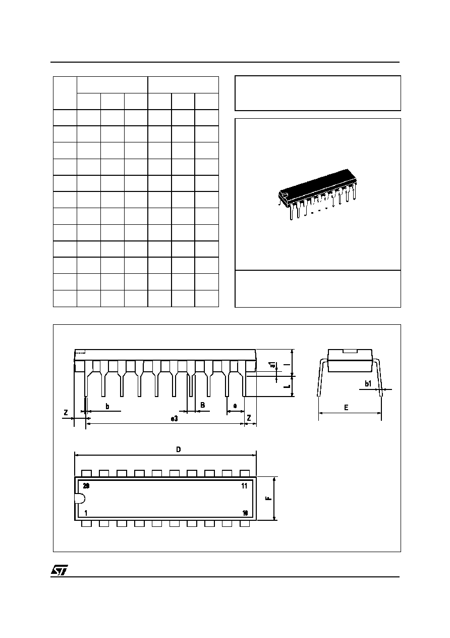
OUTLINE AND
MECHANICAL DATA
8
∞
(max.)
10
8/10
L6225
DIM.
mm
inch
MIN.
TYP.
MAX.
MIN.
TYP.
MAX.
a1
0.51
0.020
B
0.85
1.40
0.033
0.055
b
0.50
0.020
b1
0.38
0.50
0.015
0.020
D
24.80
0.976
E
8.80
0.346
e
2.54
0.100
e3
22.86
0.900
F
7.10
0.280
I
5.10
0.201
L
3.30
0.130
Z
1.27
0.050
Powerdip 20
OUTLINE AND
MECHANICAL DATA

L6225
9/10
1
1
0
11
20
A
e
B
D
E
L
K
H
A1
C
SO20MEC
h x 45
∞
SO20
DIM.
mm
inch
MIN.
TYP.
MAX.
MIN.
TYP.
MAX.
A
2.35
2.65
0.093
0.104
A1
0.1
0.3
0.004
0.012
B
0.33
0.51
0.013
0.020
C
0.23
0.32
0.009
0.013
D
12.6
13
0.496
0.512
E
7.4
7.6
0.291
0.299
e
1.27
0.050
H
10
10.65
0.394
0.419
h
0.25
0.75
0.010
0.030
L
0.4
1.27
0.016
0.050
K
0
∞
(min.)8
∞
(max.)
OUTLINE AND
MECHANICAL DATA

Information furnished is believed to be accurate and reliable. However, STMicroelectronics assumes no responsibility for the consequences
of use of such information nor for any infringement of patents or other rights of third parties which may result from its use. N o license is granted
by implication or otherwise under any patent or patent rights of STMicroelectronics. Specifications mentioned in this publication are subject
to change without notice. This publication supersedes and replaces all information previously supplied. STMicroelectronics products are not
authorized for use as critical components in life support devices or systems without express written approval of STMicroelectronics.
The ST logo is a registered trademark of STMicroelectronics
Æ
2001 STMicroelectronics - All Rights Reserved
STMicroelectronics GROUP OF COMPANIES
Australia - Brazil - China - Finland - France - Germany - Hong Kong - India - Italy - Japan - Malaysia - Malta - Morocco - Singapore - Spain
- Sweden - Switzerland - United Kingdom - U.S.A.
http:/ /www.st.com
10/10
L6225