 | –≠–ª–µ–∫—Ç—Ä–æ–Ω–Ω—ã–π –∫–æ–º–ø–æ–Ω–µ–Ω—Ç: L6238S | –°–∫–∞—á–∞—Ç—å:  PDF PDF  ZIP ZIP |
L6238S
12V SENSORLESS SPINDLE MOTOR CONTROLLER
PRODUCT PREVIEW
12V OPERATION
3A, THREE-PHASE DMOS OUTPUT
(TOTAL R
dson
0.52
)
NO HALL SENSORS REQUIRED
DIGITAL BEMF PROCESSING
LINEAR OR PWM CONTROL
STAND ALONE OR EXT. DRIVER
SHOOT-THROUGH PROTECTION
THERMAL SHUTDOWN
DESCRIPTION
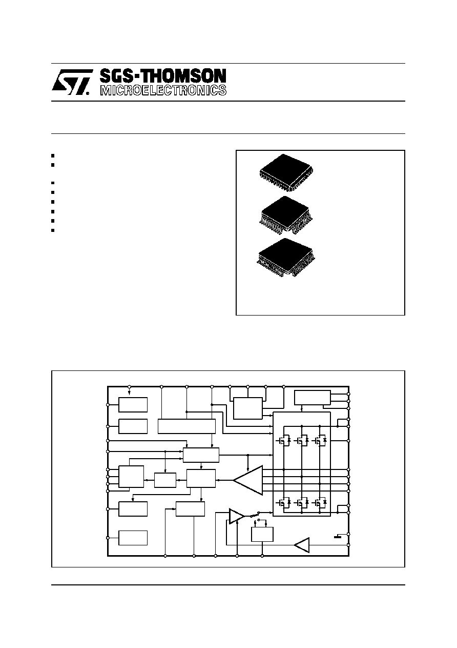
The L6238S is a Three-Phase, D.C. Brushless
Spindle Motor Driver system. This device features
both the Power and Sequence Sections.
Higher Power Applications can be activied with
the addition of an external Linear Driver, or by op-
erating the Internal Drivers in PWM.
Motor Start-Up, without the use of Hall Sensors,
can be achieved either by an internal start-up al-
gorithm or by manually sequencing the Output
Drivers, using a variety of User-Defined Start-UP
Algorithms.
Protection features include Stuck Rotor\Backward
Rotation Detection and Automatic Thermal Shut-
down.
This is advanced information on a new product now in development or undergoing evaluation. Details are subject to change without notice.
October 1995
ZERO
CROSSING
DETECTOR
ALIGN + GO
START-UP
ONE-SHOT
SLEW-CTRL
PWM
LIN
VL
THERMAL
SHUTDOWM
OT-WARN
CHARGE
PUMP
CPUMP3
CPUMP1
CPUMP2
D95IN232
BIAS
POWER
STAGE
AV=4V/V
DIGITAL
DELAY
OUT B
OUT C
CTR TAP
CSA INPUT
GND
PWM
TIM
VANALOG
+
+
+
-
BEMF
SENSE
VPOWER
BRAKE
DELAY
RSENSE1
DRV
CNTL
TDLY(0)
+
-
CSA
OUT A
GATE DRIVE
GM COMP
SYSTEM
CLOCK
SYS CLOCK
RSENSE2
VCTRL
PWM
COMP
PWM/
SLEW
SEQUENCER
FALIGN
OUTPUT
ENABLE
RUN/
BRAKE
SEQ INCR
MONO/SEQ
CTRL
TDLY(1)
TDLY(2)
MONO
DET
MASK DLY
TOGGLE
DIVIDE
BY N
SPIN
SENSE
FMTR
SEL POL
BLOCK DIAGRAM
ORDERING NUMBERS: L6238S (PLCC44)
L6238SQA (PQFP44)
L6238SQT (TQFP64)
PLCC44
PQFP44
TQF P64
1/31

ABSOLUTE MAXIMUM RATINGS
Symbol
Parameter
Value
Unit
BV
dss
Output Brakdown Voltage
17
V
V
Power
Motor Supply Voltage
15
V
V
Logic
Logic Supply Voltage
7
V
V
Analog
Analog Supply Voltage
15
V
V
in
Input Voltage
-0.3 to 7
V
C
storage
Charge Pump Storage Capacitor
4.7
µ
F
I
mdc
Motor Current (DC) (TQFP64 only)
(PLCC44 and PQFP44)
3
2.5
A
A
I
mpk
Peak Motor Current (Pulsed: T
on
= 5ms, d.c. = 10%)
5
A
P
tot
Power Dissipation at Tamb = 50
∞
C (PLCC44)
(TQFP64)
(PQFP44)
2.3
1.7
1.3
W
W
W
Ts
Storage and Junction Temperature
-40 to 150
∞
C
THERMAL DATA
Symbol
Parameter
PLCC44
PQFP44
TQFP64
Unit
R
th (j-amb)
Thermal Resistance Junction-Ambient
34
45
45
∞
C/W
Those Thermal Data are valid if the package is mounted on Mlayer board in stillair
1
2
3
5
6
4
7
8
9
10
12
11
13
14
15
16
17
39
38
37
36
34
35
33
32
31
30
29
40
41
42
44 43
23
22
21
19
18
20
28
27
26
24 25
OUTPUT
B
SPIN
SENSE
BRAKE
DELAY
CHARGE
PUMP
2
GND
RSENSE
1
GND
MASK
DELAY
VPOWER
PWM/SLEW
CENTER
TAP
GND
CHARGE PUMP 1
CHARGE PUMP 3
OUTPUT A
VANALOG
VPOWER
N.C.
TDLY(0)
TDLY(1)
TDLY(2)
GND
GND
GATE DRIVE
GM COMP
OUTPUT C
CSA INPUT
RSENSE 2
VCONTROL
N.C.
FMOTOR
VLOGIC
GND
RUN/BRAKE
OUTPUT
ENABLE
PWM/LINEAR
SELECT
POLE
OTWARN
PWM
LIMIT
TMR
PWM
COMP
FALIGN
MONO/SEQINC
CTRL
SEQ.
INCREMENT
SYSTEM
CLOCK
D95IN245
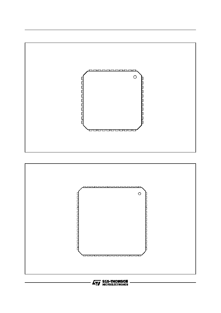
PIN CONNECTION PLCC44 (Top view)
L6238S
2/31
1
2
3
5
6
4
7
8
9
10
24
11
25
26
27
28
29
62
61
60
59
57
58
56
55
54
53
52
43
42
41
39
38
40
48
47
46
44 45
OUTPUT
A
OUTPUT
A
N.C.
VPOWER
VANALOG
VPOWER
GND
GND
GND
CHARGE
PUMP
3
CHARGE
PUMP
1
N.C.
OTWARN
SELECT POLE
PWM LIMIT TMR
OUTPUT ENABLE
PWM/LINEAR
RUN/BRAKE
SEQ. INCREMENT
SYSTEM CLOCK
MONO/SEQINC CTRL
FALIGN
CHARGE PUMP 2
RSENSE 1
RSENSE 1
BRAKE DELAY
OUTPUT B
SPIN SENSE
OUTPUT B
PWM/SLEW
CENTER TAP
VPOWER
VPOWER
OUTPUT
C
OUTPUT
C
N.C.
RSENSE
2
CSA
INPUT
RSENSE
2
GND
GND
GND
GM
COMP
GATE
DRIVE
D95IN244
19
20
21
22
23
30
31
32
51
50
49
PWM COMP
N.C.
GND
MASK DELAY
GND
GND
64
63
GND
N.C.
GND
GND
17
18
12
13
14
15
16
37
36
34
33
35
TDLY(0)
TDLY(1)
GND
GND
TDLY(2)
VCONTROL
FMOTOR
GND
GND
VLOGIC
PIN CONNECTION TQFP64 (Top view)
1
2
3
5
6
4
7
8
9
10
17
11
18
19
20
21
22
44
43
42
41
39
40
38
37
36
35
34
28
27
26
24
23
25
33
32
31
29 30
VANALOG
N.C.
TDLY(0)
TDLY(2)
GND
TDLY(1)
GND
CHARGE
PUMP
1
CHARGE
PUMP
3
VPOWER
OUTPUT
A
OTWARN
SELECT POLE
PWM LIMIT TIMER
PWM/LINEAR
RUN/BRAKE
OUTPUT ENABLE
SEQ. INCREMENT
SYSTEM CLOCK
MONO/SEQINC CTRL
FALING
PWM COMP.
GND
CHARGE PUMP 2
RSENSE 1
BRAKE DELAY
OUTPUT B
SPIN SENSE
PWM/SLEW
CENTER TAP
VPOWER
MASK/DELAY
GND
CSA
INPUT
VCONTROL
N.C.
VLOGIC
GND
FMOTOR
GND
GATE
DRIVE
GM
COMP
RSENSE
2
OUTPUT
C
D95IN243
12
13
14
15
16
PIN CONNECTION PQFP44 (10x10) (Top view)
L6238S
3/31

PIN FUNCTIONS
PLCC44 PQFP44 TQFP64
Name
I/O
Function
1
39
56, 57
OUTPUT B
I/O
DMOS Half Bridge Output and Input B for Bemf sensing.
2
40
58
SPIN SENSE
O
Toggless at each Zero Crossing of the Bemf.
3
41
59
BRAKE DELAY
I
Energy Recovery time constant, defined by external R-C to ground.
4
42
60, 61
R
sense 1
O
Outputs A+B connections for the Motor Current Sense Resistor
to ground
5
43
62
CHARGE
PUMP 2
I
Negative Terminal of Pump Capacitor.
6, 7,
17, 29,
39, 40
1, 11,
23, 33,
34, 44
*
GROUND
S
Ground terminals.
8
2
4
CHARGE PUMP 1
I
Positive terminal of Pump Capacitor.
9
3
5
CHARGE PUMP 3
O
Positive terminal of Storage Capacitor.
10
4
6, 7
OUTPUT A
I/O
DMOS Half Bridge Output and Input A for Bemf sensing.
11, 42
5, 36
9, 10,
52, 53
V
power
S
Power Section Supply Terminal.
12
6
11
V
analog
S
12V supply.
13, 32
7, 26
8, 18,
19, 31,
41
N.C
N.C
Open Terminal
14
8
12
Tdly(0)
I
Three bits that set the Delay between the detection of the Bemf
zero crossing, and the commutation of the next Phase.
15
9
13
Tdly(1)
I
16
10
14
Tdly(2)
I
18
12
20
OTWARN
O
Overtemperature Warning Output
19
13
21
SELECT POLE
I
Selects # of Motor Poles. A zero selects 8, while a one selects 4
poles.
20
14
22
PWM TIMER
I
Capacitor connected to this pin sets the maximum time allowed
for 100% duty cycle during PWM operation
21
15
23
PWM/LINEAR
I
Selects PWM or Linear Output Current Control
22
16
24
OUTPUT
ENABLE
I
Tristates Power Output Stage when a logic zero.
23
17
25
SEQUENCE
I
Rising edge will initiate start-up. A Braking rountine is started
when this input is brought low.
24
18
26
SEQ
INCREMENT
I
A low to high transition on this pin increments the Output State
Sequencer.
25
19
27
SYSTEM CLK
I
Clock Frequency for the system timer/counters.
26
20
28
MONO/SEQ.
INC. CONTROL
I
A logic one will disable the Monotonicity Detector and Sequence
Increment functions.
27
21
29
Falign
I
Reference Frequency for the opt. Auto-Start Algorithm. If int.
start up is not used, this pin must be connected to the System
Clock.
28
22
30
PWM COMP
O
Output of the PWM Comparator
30
24
35
Vlogic
S
5V Logic Supply Voltage.
31
25
36
Fmotor
O
Motor Once-per-Revolution signal.
33
27
37
Vcontrol
I
Voltage at this input controls he Motor Current
34
28
38
CSA INPUT
I
Input to the Current Sense Amplifier.
35
29
39, 40
Rsense 2
O
Output C connection for the Motor Current Sense Resistor to
ground.
36
30
42, 43
OUTPUT C
I/O
DMOS Half Bridge Output and Input C for Bemf sensing.
37
31
44
gm COMP
I
A series RC network to ground that defines the compensation of
the Transconductance Loop.
L6238S
4/31

PIN FUNCTIONS
PLCC44 PQFP44 TQFP64
Name
I/O
Function
38
32
45
GATE DRIVER
I/O
Drivers the Ext. PFET Gate Driver for Higher Power applications.
This pin must be grounded if an external driver is not used.
41
35
51
MASK/DELAY
O
Internal Logic Signals used for production Testing
43
37
54
CENTER TAP
I
Motor Center Tap used for differential BEMF sensing.
44
38
55
PWM/SLEW
I
R/C at this input set the Linear Slew Rate and PWM OFF-Time
0.0
0.3
1.0
3.0
Cb(
µ
F)
0.0
0.3
1.0
3.0
T
BD
(s)
D95IN274
Figure 1: Brake Delay Timeout vs C
brake
(R
brake
= 1Meg)
10
30
100
300
Rs(K
)
0.0
0.3
1.0
3.0
S
VR
(V/
µ
s)
D95IN275
Figure 2: Linear Slew Rate vs R
slew
100
300
Coff(pF)
1
3
10
30
PWM
(
µ
s)
D95IN276
Figure 3: PWM Off - Time vs R
slew
/C
off
100
300
Ctimer(pF)
10
30
PWM
(
µ
s)
D95IN277
Figure 4: PWM Limit Time - Out vs C
timer
L6238S
5/31
ELECTRICAL CHARACTERISTICS (T
amb
= 0 to 70
∞
C; V
A
= V
Pwr
= 12V; V
logic
= 5V; unless otherwise
specified)
Symbol
Parameter
Test Condition
Min.
Typ.
Max.
Unit
GENERAL
V
analog
Analog Supply Voltage
10.5
13.5
V
I
analog
Analog Supply Current
Run Mode V
A
= 13.5V
1.5
2.7
4.5
mA
Brake Mode V
A
= 13.5V
280
800
µ
A
V
logic
Logic Supply Voltage
4.5
5.0
5.5
V
I
log ic
Logic Supply Current
Run Mode V
logic
= 5.5V
1
2
3.2
mA
Brake Mode
100
500
1000
µ
A
THERMAL SHUTDOWN
* T
sd
Shut Down Temperature
150
180
∞
C
* T
hys
Recovery Temperature
Hysteresis
30
∞
C
* T
ew
Early Warning Temperature
T
sd
-25
∞
C
POWER STAGE
R
DS(on)
Output ON Resistance per FET
T
j
= 25
∞
C; V
A
= 10.5V
T
j
= 125
∞
C; V
A
= 10.5V
0.20
0.26
0.40
I
o(leak)
Output Leakage Current
V
pwr
= 15V
1
mA
V
F
Body Diode Forward Drop
I
m
= 2.0A
1.5
V
dVo/dt
Output Slew Rate (Linear)
R
slew
= 100K
0.15
0.30
0.45
V/
µ
s
Output Slew Rate (PWM)
10
150
V/
µ
s
I
gt
Gate Drive for Ext. Power
DMOS
V
control
= 1V; V
sns
= 0V;
V
A
= 10.5V
4.5
mA
V
Gate-Drive
Ext Driver Disable Voltage
0.7
V
V
Ctrl-Range
Voltage Control Input Range
0
5.0
V
I
in(VCtrl)
Voltage Control Input Current
10
µ
A
PWM OFF-TIME CONTROLLER (R
slew
= 100K
, C
off
= 120pF)
T
off
OFF Time
9
11
14
µ
s
V
chrg
Capacitor Charge Voltage
V
A
= 10.5V
2.31
2.65
3.1
V
V
trip
Lower Trip Threshold
1.25
V
PWM LIMIT TIMER
I
chrg
Capacitor Charge Current
V
PWM Timer
= 0V; V
A
= 10.5V
10.0
20.0
30
µ
A
V
chrg
Capacitor Charge Voltage
V
A
= 10.5V
3.0
3.5
4.0
mV
V
trip
Lower Trip Threshold
100
400
V
BEMF AMPLIFIER
Z
inCT
Center Tap Imput Impedance
20
30
40
K
V
Bemf
Minimum Bemf (Pk-Pk)
60
mV
CURRENT SENSE AMPLIFIER
I
snsin
Input Bias Current
V
A
= 13.5V
10
µ
A
G
v
Voltage Gain
3.8
4.0
4.2
V/V
SR
Slew Rate
0.33
0.8
V/
µ
s
L6238S
6/31

ELECTRICAL CHARACTERISTICS (Continued)
Symbol
Parameter
Test Condition
Min.
Typ.
Max.
Unit
BRAKE DELAY
V
chrg
Capacitor Charge Voltage
R
T
= 50K
8.8
9.6
10.5
V
I
in
Input Current
V
in
= 5.0V
500
nA
I
out3
Source Current
V
A
= 10.5V
0.5
mA
V
Thres
Delay Timer Low Trip Threshold
1.2
1.8
2.8
V
CHARGE PUMP
V
out
Storage Capacitor Output
Voltage
V
A
= 10.5V; I
out
= 500
µ
A
17
V
F
cp
Charge Pump Frequency
140
450
KHz
I
in
Vstorage Input Current (Run
Mode)
V
storage
= 12V; V
A
= V
logic
= 0
25
µ
A
I
brkdly
Vstorage Leakage Current
(Brake Delay Mode)
V
storage
= 12V; V
A
= V
logic
= 0
0.4
1
µ
A
I
brake
Vstorage Leakage Current
(Brake Mode)
V
storage
= 12V; V
A
= V
logic
= 0
0.1
1
µ
A
SEQUENCE INCREMENT
t
seq
Time Between Rising Edges
1
µ
s
OUTPUT TRANSCONDUCTANCE AMPLIFIER Note: Measure at OTA Comp. pin.
V
oh
Voltage Output High
V
A
= 10.5V
10
V
V
outL
Output Voltage
2.0
V
I
source
Output Voltage
40.0
0.5
V
I
sink
Output Sink Current
40.0
µ
A
LOGIC SECTION
V
inH
V
inL
Input Voltage (All Inputs
Except Run/Brake
V
logic
= 4.5 to 5.5V
3.5
1.5
V
V
V
inH
V
inL
Run/Brake Input Voltage
V
logic
= 4.5 to 5.5V
2.0
1.0
V
V
I
inH
I
inL
Input Current
-1.0
1.0
µ
A
mA
V
outL
V
inL
Output Voltage
Vsink = 2.0mA
V
source
= 2.0mA
4.5
0.5
V
V
F
sys
System Clock Frequency
8.0
12.0
MHz
t
off
/t
on
Clock ON/OFF Time
20
ns
Tdelay (2)
Tdelay (1)
Tdelay (0)
Commutation Phase Delay,
in Electrical Degrees
1
0
1
2.0
1
0
0
9.4
1
1
1
18.80
1
1
0
20.68
0
0
1
22.56
0
0
0
24,44 (*)
0
1
1
26.32
0
1
0
28.20
(*) Input Default
Phase Delay Truth Table
L6238S
7/31

FUNCTIONAL DESCRIPTION
1.0 INTRODUCTION
1.1 Typical Application
In a typical application, the L6238S will operate in
conjunction with the L6244 Voice Coil Driver as
shown in Fig. 1-1.
This configuration requires a minimum amount of
external components.
1.2 Input Default States
Figure 1-2 depicts the two possible input struc-
tures for the logic inputs. If a particular pin is not
OUT
A
10
CTR
TAP
43
OUT
B
1
OUT
C
36
RSENSE
4.35
CSA
34
6.33
10nF
5
8
CHRG
PUMP
2
CHRG
PUMP
1
8.12MHz
4.7
µ
F
25
9
CHRG
PUMP
3
SYS
CLK
22
µ
F
F
ALIGN
V
PWR
27
11,42
400pF
44
PWM
SLEW
100K
10K
37
0.068
µ
F
GM
COMP
0.1
µ
F
3
BRK
DLY
6,7,17,
29,39,40
GND
60-90Hz
Note:
If
the
internal
Start-up
Algorithm
is
not
used,
connect
this
pin
to
SYS_CLK
V
ANLG
12V
V
LOGIC
VLOGIC(5V)
12
39
L6238S
SPINDLE
MOTOR
DRIVER
CONTROLLER
220pF
20
16
15
14
18
31
34
33
23
22
38
26
GATE
DRV
MONO
SEQ.
OUT
ENA
RUN/BRK
V
CTRL
SEQ
INC
F
MTR
OT
WARM
T
DLY(0)
T
DLY(1)
T
DLY(2)
PWM
TMR
19
data(0)
20
data(1)
21
data(2)
22
data(3)
23
data(4)
24
data(5)
25
data(6)
26
data(7)
36
WR
28
A0
27
A1
18
CS
43
35
10K
V
LOGIC
POR
44
9
3
7
GATE
DRIVE
42
Vpower
1
µ
F
0.068
µ
F
3.6K
27K
0.1
µ
F
VCM
Rs
0.4
38
4
5
8
360K
12
360K
13
360K
14
10K
11
100K
10
15
6,7,17,29,39,40
41
31
4
3
1
3
3
GND
POR
DLY
Rprogram
V
PROG
V
CC/2
GAIN2-IN
DA0Out
GAIN1-IN
ERROR
AMP
OUTPUT
V
PUMP
CP2
CP1
0.01
µ
F
D95IN278
L6244
VOICE
COIL
DRIVER
DA2
OUT
SENSE
OUT
OUT
B
SENSE
+INPUT
SENSE
-INPUT
OUT
A
V
CC
SENSE
Figure 1-1
L6238S
8/31

used in an application, it may either be connected
to ground or VLOGIC as required, It may also be
simply left unconnected.
If no connection is made, the pin is either pulled
high or low by internal constant current gener-
ators as shown above.
A listing of the logic and clock inputs is shown in
Table 1 with the corresponding default state.
1.3 Modes of Operation
There are 5 basic modes of operation.
1) Tristate
When Output Enable is low, the output power
drivers are tristated.
2) Start-Up
With Output Enable high, bringing Run/Brake
from a low to a high will energize the motor and
the system will be driven by the Fully-Integrated
StartUp Algorithm.
A user-defined Start-Up Algorithm, under control
of a MicroProcessor, can also be achieved via the
sequence increment input.
3) Run
Run mode is achieved when the motor speed
(controlled
by
the
external
microprocessor)
reaches the nominal speed.
4) Park
When Run/Brake is brought low, energy to park
the heads may be derived from the rectified Bemf.
The energy recovery time is a function of the
Brake Delay Time Constant. In this state, the qui-
escent current of the device is minimized (sleep
mode).
5) Brake
After the Energy Recovery Time-Out, the device
is in Brake, with all lower Drivers in full conduc-
tion.
There are two mutually exclusive conditions
which may be present during the Tristate Mode
(wake up):
a)the spindle is stopped.
b)the system is still running at a speed that
allows for resynchronization.
In order to minimize the ramp up time, the micro-
controller has the possibility to:
check the SPIN SENSE pin, (which toggles at
the Bemf zero crossing frequency)
enable the power to the motor based on the
previous information. Otherwise the
µ
P may is-
sue a Brake command, followed by the start-
up procedure after the motor has stopped spin-
ning.
2.0 STATE DIAGRAMS
2.1 State Diagram
Figure 2-1 is a complete State Diagram of the
controller depicting the operational flow as a func-
tion of the control pins and motor status. The flow
can be separated into four distinct operations.
2.2 Align + Go
Figure 2-2 represent the normal flow that will
achieve a spin-up of the spindle motor using the
internally generated start up algorithm.
Upon
power
up,
or
from
any
state
with
Run/Brake low the controller first sets the state
machine for State=1 with the Outputs Tristated.
The period counter that monitors the time be-
tween zero crossing is stopped, analog with the
phase and mask delay counters.
When Run/Brake is brought high, the motor is in
the first part of the align mode at State 2 (Output
A high and Output C low). If Output Enable is
high, the controller first checks to determine if the
motor is still spinning for a time of 21
(with
Sys_Clk = 10MHz). The drivers are now enabled
and after the align time-out, (64/Falign), the se-
quencer double increments the outputs to State 4
(Output B high and Output A low). The first part
of this align mode is used to reduce the effects of
stiction
Pin Function
Configuration
Tdly (0,1,2)
Pull-Down
Select Pole
Pull-Down
PWM/Linear
Pull-Down
Output Enable
Pull-Down
Run/Brake
Pull-Up
Sequence Increment
Pull-Down
System Clock
Pull-Up
Faling
Pull-Up
Table 1
330
V
LOGIC
10
µ
A
330
V
LOGIC
10
µ
A
PULL-UP
PULL-DOWN
D95IN279
Figure 1-2
L6238S
9/31

After the next align time-out 192/Falign), the con-
troller enters the Go mode, were the sequencer
again double increments the output phase upon
detection of the motor's Bemf.
The align time-out may be optimized for the appli-
cation by changing the Faling reference fre-
quency.
A Watch-Dog Timer protection feature is built into
the control logic to monitor the Falign pin for a
clocking signal. This circuitry, shown in Figure 2-3
will prevent start up the device if the Falign clock
is not present.
Without this feature, the output would remain in
the first phase under high current conditions, if
the clock were not present.
If the external sequencer is used to provide start
up, the system clock may be tied to the Falign pin
to satisfy the requirements of the Watch-Dog
Timer.
2.3 Resynchronization
If power is momentarily lost, the sequencer can
automatically resynchronize to the monitored
STATE = 1
DRIVERS OFF
MIN CLOCK DELAY
PERIOD STOP
DELAY STOP
MASK STOP
SEQLNC=1 &
OUTENA=0
RUN/BRK=X
INT. START-UP DISABLED
MIN. CLOCK DELAY
LOAD MIN. DELAY
LOAD MIN. MASK***
RUN/BRK=1 &
OUTENA=1
DRIVERS ON
PERIOD COUNT
DELAY COUNT
STATE=STATE+1*
MASK COUNT
MASK COUNT
SEQINC=0
SEQINC=1
LOAD DELAY=PERIOD
LOAD MASK=PERIOD
RESET PERIOD
PERIOD COUNT
DELAY COUNT**
BEMF
BEMF
SEQINC=0
SEQINC=1
RUN/BRAKE=1
RUN/BRAKE=0
FROM ANY STATE
DRIVERS OFF
MIN CLOCK DELAY
LOAD MIN MASK***
PERIOD STOP
DELAY COUNT
STATE=STATE+1
MASK COUNT
LOAD MIN. DELAY
LOAD MIN. MASK***
DELAY COUNT
STATE=STATE+1
MASK COUNT
BEMF
STATE=STATE+1
SEQINC=1
RETURN TO
PREVIOUS STATE
(CHANGING SEQINC=1)
BEMF
FROM ANY STATE
WITH SEQ_INC=0
* VALID IF SEQINC=0, AND DELAY TIMES OUT
** CLOCK DELAY=F(TDLY_[2:0])
WHEN BEMF PERIOD <3.3ms @ 10MHz
(SPEED >12.7Hz FOR 8 POLES)
STATE=STATE+2
CHECK FOR Zc
BEMF
DRIVERS OFF
STATE=STATE+1
MIN CLOCK DELAY
LOAD MIN DELAY
LOAD MAX MASK
DELAY COUNT
STATE=STATE+1
MASK COUNT
OUTENA=1
OUTENA=1
OUTENA=1
DRIVERS OFF
MIN CLOCK DELAY
PERIOD STOP
DRIVERS ON
PERIOD STOP
DELAY STOP
MASK STOP
STATE=STATE+2
STATE=STATE+1
LOAD DELAY=MIN
LOAD MASK=MAX
PERIOD COUNT
DELAY COUNT
STATE=STATE+1
MASK COUNT
BEMF
LOAD DELAY=MIN
LOAD MASK=MIN
RESET PERIOD
PERIOD COUNT
DELAY COUNT*
STATE=STATE+1
MASK COUNT
2
21
SYS_CLK
2
21
SYS_CLK
DRIVERS OFF
RUN/BRK=0
DRIVERS OFF
RUN/BRK=0
DRIVERS ON
LOAD DELAY=PERIOD
LOAD MASK=PERIOD
RESET PERIOD
PERIOD COUNT
DELAY COUNT*
STATE=STATE+1
MASK COUNT
DRIVERS OFF
MIN CLOCK DELAY
PERIOD STOP
OUTENA=0
BEMF
MONO=0**
BEMF
OUTENA=1
OUTENA=1
BEMF
ALIGN &
GO MODE
RESYNCHRONIZATION
MODE
RUN
MODE
* CLOCK DELAY=F(TDLY [2:0] WHEN BEMF PERIOD <3.3ms @ 10MHz (SPEED>12.7Hz FOR 8 POLES)
BEMF: BEMF RISING WITH PNSLOPE=1 OR BEMF FALLING WITH PNSLOPE=0
BEMF1: BEMF RISING WITH PNSLOPE=0 OR BEMF FALLING WITH PNSLOPE=1
**MONO=0 WHEN FREQ(BEMF)=2*FREQ(PHASE)
***MIN MASK=192/SYS_CLK(I.E. WITH SYS_CLK=10MHz,MIN MASK=19.2
µ
s)
D95IN280
192/FALIGN
64/FALIGN
OUTENA=0
2
21
SYS_CLK
OUTENA=0
OUTENA=1
BEMF
POR=0
FROM ANY STATE
(FOR IS GENERATED INTERNALLY
BY MONITORING VLOGIC)
Figure 2-1
L6238S
10/31

Bemf. This resychronization can either occur
whenever Output Enable or Run/Brake is first
brought low then high.
Referring to figure 2-4, the "Hold for Resync"
state is brought low. The controller leaves this
state and enters "Start Resync" when Output En-
able is high.
S
Q
Q
TO START-UP
LOGIC
S
OVER TEMP SHUTDOWN
D95IN311
OUTPUT
ENABLE
RUN/
BRAKE
FALIGN
Figure 2.3: Watch-Dog Timer
LOAD MIN DELAY
LOAD MIN MASK***
DELAY COUNT
STATE=STATE+1
MASK COUNT
LOAD DELAY=MIN
LOAD MASK=MIN
PERIOD COUNT
DELAY COUNT*
STATE=STATE+1
MASK COUNT
CHECK FOR Zc
OUTENA=1
BEMF
DRIVERS OFF
MIN CLOCK DELAY
PERIOD STOP
D95IN312
*CLOCK DELAY=(TDLY [2:0] WHEN BEMF PERIOD <3.3ms @ 10MHz (SPEED>12.7Hz FOR 8 POLES)
BEMF: BEMF RISING WITH PNSLOPE=1 OR BEMF FALLING WITH PNSLOPE=0
BEMF: BEMF RISING WITH PNSLOPE=0 OR BEMF FALLING WITH PNSLOPE=1
** MONO=0 WHEN FREQ (BEMF)=2*FREQ(PHASE)
*** MIN MASK=192/SYS_CLK(I.E.WITH SYS_CLK=10MHz, MIN MASK=19.2
µ
s)
BEMF
RUN/BRK=0
BEMF
BEMF
DRIVERS OFF
DRIVERS ON
LOAD DELAY=PERIOD
LOAD MASK=PERIOD
RESET PERIOD
PERIOD COUNT
DELAYH COUNT*
STATE=STATE+1
MASK COUNT
MONO=0**
BEMF
BEMF
RUN
MODE
OUTENA=0
OUTENA=1
HOLD FOR RESYNC
RESYNCHRONIZATION MODE
Figure 2-4
STATE=1
DRIVERS OFF
MIN CLOCK DELAY
PERIOD STOP
DELAY STOP
MASK STOP
DRIVERS OFF
MIN CLOCK DELAY
LOAD MIN DELAY
LOAD MIN MASK
PERIOD STOP
DELAY COUNT
STATE=STATE+1
MASK COUNT
CHECK FOR Zc
DRIVERS ON
PERIOD STOP
DELAY STOP
MASK STOP
STATE=STATE+1
LOAD DELAY=MIN
LOAD MASK=MAX
PERIOD COUNT
DELAY COUNT
STATE=STATE+1
MASK COUNT
CHECK FOR Zc
BEMF
2
21
SYS_CLK
RUN/BRAKE=1
POR=0
FROM ANY STATE
OUTENA=1
64/FALIGN
192/FALIGN
DRIVERS ON
LOAD DELAY=PERIOD
LOAD MASK=PERIOD
RESET PERIOD
PERIOD COUNT
DELAY COUNT*
STATE=STATE+1
MASK COUNT
BEMF
D95IN310
BEMF: BEMF RISING WITH PNSLOPE=1 OR BEMF FALLING WITH PNSLOPE=0
BEMF: BEMF RISING WITH PNSLOPE=0 OR BEMF FALLING WITH PNSLOPE=1
***MIN MASK=192/SYS_CLK (I.E. WITH SYS_CLK=10MHz, MIN MASK=19.2
µ
s)
BEMF
RUN/BRK=0
FROM ANY STATE
Figure 2.2
L6238S
11/31

If zero crossings are detected, the sequencer will
automatically lock on to the proper phase.
This resynchronization will take effect with the
motor speed running as low as typically 30% of
it's nominal value.
2.5 External Sequencing
Although the user-defined Start-Up Algorithm is
flexible and will consistently spin up a motor with
no external interaction, the possibility exists
where certain applications might require complete
microprocessor control of start-up.
The L6238S offers this capability via the SE-
QUENCE INCREMENT input. Referring to figure
2-5, during initial power-up with Output Enable
low, the controller is in the "Hold and Wait for De-
cision" state. If the SEQUENCE INCREMENT pin
is brought high during this state, the Auto StartUp
Algorithm is disabled and the sequencer can be
controlled externally.
When Output Enable and Run/Brake are
brought high, the sequencer is incremented on
each positive transition o the SEQUENCER IN-
CREMENT pin. During the time that this pin is
high, all Bemf information is masked out. When it
is low, the Bemf information can be detected nor-
mally after the internal mask time. The minimum
mask time is 192/Sys_Clk (i.e. with Sys_Clk =
10MHz, min. mask = 19.2
µ
s) Therefore to insure
that the sequencer is under complete control of
the state machine, the time that the SEQUENCE
INCREMENT pin is held low should be much less
then the min. mask time, but greater then 1
µ
s.
When the motor has reached a predetermined
speed, the SEQUENCE INCREMENT pin can be
left low and the L6238S Motor Control logic will
take over and automatically spin up the motor to
the desired speed
.
3.0 START-UP ALGORITHMS
3.1 Spin-Up Operation
The spin operation can be separated into 3 parts:
1) Open Loop Start-Up - The object is to create
motion in the desired direction so that the Bemf
voltages at the 3 motor terminals can provide reli-
able information enabling a transition to closed
loop operation.
STATE=1
DRIVERS OFF
MIN CLOCK DELAY
PERIOD STOP
DELAY STOP
MASK STOP
INT START-UP DISABLED
MIN CLOCK DELAY
LOAD MIN DELAY
LOAD MIN MASK
MASK COUNT
SEQINC=1 &
OUTENA=0
RUN/BRK=X
D95IN313
*VALID IF SEQINC=0, AND DELAY TIMES OUT
**CLOCK DELAY=F(TDLY_[2:0])
WHEN BEMF PERIOD <3.3ms @ 10MHz (SPEED >12.7Hz FOR 8 POLES)
SEQINC=0
STATE=STATE+1
MASK COUNT
LOAD DELAY=PERIOD
LOAD MASK=PERIOD
RESET PERIOD
PERIOD COUNT
DELAY COUNT**
BEMF
POR=0
FROM ANY STATE
DRIVERS ON
PERIOD COUNT
DELAY COUNT
SEQINC=0
BEMF
SEQINC=1
STATE=STATE+1
SEQINC=1
FROM ANY STATE
WITH SEQ_INC=0
RETURN TO
PREVIOUS STATE
(CHANGING SEQINC=1)
RUN/BRK=1 &
OUTENA=1
SEQINC=1
Figure 2-5
L6238S
12/31

2) Closed Loop Start-Up - The Bemf voltage
zerocrossings provide timing information so that
the motor can be accelerated to steady state
speed.
3) Steady-State Operation - The Bemf voltage
zero-crossings provide timing information for pre-
cision speed control.
The L6238S contains features that offer flexible
control over the start-up procedure. Either the on-
board Auto-Start Algorithm can be used to control
the start-up sequence or more sophisticated ex-
tenal start-up algorithms can be developed using
the Serial Port and key control/sense functions
brought out to pins.
3.2 Auto-Start Algorithm
When initially powered up, the controller defaults
to the internal AutoStart Mode. When Run/Brake
is low, the L6238S is in brake mode, and the
Auto-Start Algorithm is reset. In the brake mode,
all of the lower DMOS drivers are ON, and the up-
per drivers are OFF.
The Auto-Start Algorithm is based on an Align &
Go approach and can be visualized by referring to
Figure 3-1. Shown are the Run/Brake control sig-
nals, sequencer function, and the three output
voltage waveforms.
Referring to figure 3-1, the following is the se-
quence of events during Auto-Start:
With Output Enable = 1, Run/Brake = 0
- State Machine is set to State 1 with the drivers
Trisatted.
Alignment Phase (1)
Run/Brake = 1
- Output Stage is sequenced to State 2 and the
drivers energized with OUTPUT A high and
OUTPUT C low for 64/Falign seconds.
Alignment Phase (2)
- Output Stage is double sequenced to State 4
with OUTPUT B high and OUTPUT A low for
STATE 2
A=HIGH
B=FLOAT
C=LOW
STATE 4
A=LOW
B=HIGH
C=FLOAT
STATE 6
A=FLOAT
B=LOW
C=HIGH
500ms/DIV
* FALIGN=90Hz
A
OUT
1
10V
B
OUT
2
10V
C
OUT
3
10V
ALIGNMENT
GO
DOUBLE INCREMENTS
*0.711s
*2.133s
RUN/BRAKE
SEQUENCER
D95IN314
Figure 3-1: Align+Go
L6238S
13/31

192/Falign seconds.
- During the alignment phase, the SEQ INCRE-
MENT signal is ignored.
Go Phase
- The internal sequencer double increments the
output stage to State 6, which should produce
torque in the desired direction.
- with SEQ INCREMENT held low, the se-
quencer is now controlled by the Bemf zero
crossings, and the motor should ramp up to
speed.
3.3 Externally Controlled Start-Up Algorithms
Enhanced Start-Up Algorithms can be achieved
by using a
µ
Processor to interact with the
L6238S.' The L6238S has the ability to transition
to Closed Loop Start-Up at very low speeds, re-
ducing the uProcessor task to monitoring status
rather than real time interaction. Thus, it is a per-
fect application for an existing
µ
Processor.
The following control and status signals allow for
very flexible algorithm development:
SEQ_INCR A low to high transition at this input
is used to increment the state of the power out-
put stage. It is useful during start-up, because
the
µ
Processor can cycle to any desired state,
or cycle through the states at any desired rate.
When held high, it inhibits the BEMF zero
crossings from incrementing the internal se-
quencer.
SPIN SENSE This output is low until the first
detected Bemf zero crossing occurs. It then
toggles at each successive zero crossing. This
signal serves as a motion detector and gives
useful timing information as well as the slope
of the Bemf.
3.4 Start Up Approaches
Align & Go Approach The Align & Go approach
provides a very time efficient algorithm by ener-
gizing the coils to align the rotor and stator to a
known phase. This approach can be achieved via
the sequencing SEQ INCR. SPIN SENSE can be
monitored to assure that motion occurred. Once
ample time is given for alignment to occur, SEQ
INCR can be double incremented, and the SPIN
SENSE pin can be monitored to detect motion.
When SEQ INCR is pulled low, control is trans-
ferred to the internal sequencer, and the L6238S
finishes the spinup operation. If no motion is de-
tected, SEQ INCR can be incremented to a differ-
ent phase and the process can be repeated. The
alignment phase may cause backward rotation,
which on the average will be greater than the
Stepper Motor approach.
The Auto-Start algorithm described earlier is an
Align & Go approach. The main advantages of
the integrated Auto-Start are that the
µ
P is not in-
volved real-time, and there are a minimum of in-
terface pins required to the spindle control sys-
tem.
Stepper Motor Approach This approach mini-
mizes backward rotation by sequencing SEQ
INCR at an initial rate that the rotor can follow.
Thus, it is driven in a similar fashion to a stepper
motor. The rate is continually increased until the
Bemf voltage is large enough to reliably use the
zero-crossings for commutation timing. SEQ
INCR is held low, causing control to be passed to
the L6238S's internal sequencer as in the Align &
Go approach.
The Stepper Motor approach takes longer than
the Align & Go approach because the initial com-
mutation frequency and subsequent ramp rate
must be low enough so that the motor can follow
without slipping. This implies that to have a reli-
able algorithm, the initial frequency and ramp rate
must be chosen for the worst case motor under
worst case conditions.
4.0 MOTOR DRIVER
4.1 Output Stage
The output stage forms a 3-Phasefull wave bridge
consisting of six Power DMOS FET High output
currents are allowed for bbrief periods. High out-
put currents are allowed for brief periods. Output
Power exceeding the stand-alone power dissipa-
tion capabilities of the L6238S can be increased
with the addition of an external P-FET or by the
use of Pulse-Width-Modulation.
Table 4-1 is a reference diagram that lists the pa-
rameters associated with 8-pole motors operating
at 3600 and 5400 RPM.
Figure 4-1 represents the waveforms associated
with the output stage. The upper portion of figure
4-1 shows the flow of current in the motor wind-
ings for each of the 24 phase increments. A rota-
tional degree index is shown as a reference along
with a base line to indicate the occurrence of a
zero crosing. The output waveforms are a digitally
reproduced voltage signals as measured on sam-
ples.The feedback Input is multiplexed between
the internal Bemf Zero Crossing Detector and an
externally provided sync pulse (EXT INDEX)
Shown in figure 10 is the classical state diagram
for a phase detector along with waveform exam-
ples.
A typical
sequence starts when the outputs
switch states. Referring to figure 4-1, during
phase 1, output A goes high, while outputB is low.
During this phase, output C is floating, and the
Bemf is monitored. The outputs remain in this
state for 60 electrical degrees as indicated by the
first set of dashed lines. After this period the out-
L6238S
14/31

Table 4-1
Rotational Speed
3600rpm
5400rpm
Rotational Frequency
60Hz
90Hz
Rotational Period
16.667ms
11.111ms
Electrical Period
4.167ms
2.778ms
Phase Period
694.5
µ
s
463.0
Figure 4-1: Waveforms
L6238S
15/31

put switched to phase 2 with output A high and C
low with the Bemf amplifier monitoring output B.
In order to prevent commutation current noise be-
ing detectedm as a false zero crossing, a mask-
ing circuit automatically blanks out all incoming
signals as soon as a zero crossing is detected.
When the next commutation occurs an internal
counter starts counting down to set the time that
the masking pulse remains.
The counter is initially loaded with a number that
is equal to time that is always 25% of the previous
phase period or 15 electrical degrees. The time-
out of the masking pulse shown for reference at
the bottom of figure 4-1. Thus the actual masking
period is the total of the time from the detected
zero crossing to the phase commutation, plus
25% of the previous period. The mask pulse op-
eration is further discussed in section 4.6, Slew
Rate Control and PWM operation.
After the masking period, the Bemf voltage at out-
put B is monitored for a zero crossing. Upon de-
tection of the crossing, the output is commutated
after the selected phase delay insuring maximum
torque. The spin sense waveform at the bottom of
the figure indicates that this output signal toggles
with each zero crossing.
4.2 Brake Delay
When Run/Brake is brought low, a brake is initi-
ated. Referring to figure 4-2, SW1 is opened and
the brake delay capacitor, C
brake
, is allowed to
discharge towards groun via R
brake
.
At the same time, switches SW2 through SW7
bring the gates of the output FETs to ground halt-
ing conduction, causing the motor to coast. While
the motor is coasting, the Bemf is used to park
the heads. When Cbrake reaches a voltage that
is below the turn ON threshold of Q1, Switches
SW8, 9, and 10 bring the gates of the lower driv-
ers to V
brake
potential. This enables the lower
FETs causing a braking action.
The analog and logic supplies are not monitored
in the L6238S, since the L6244 already monitors
this voltage and initiates a Park function when
either supply drops to a predeterminated level.
Figure 4-2
L6238S
16/31
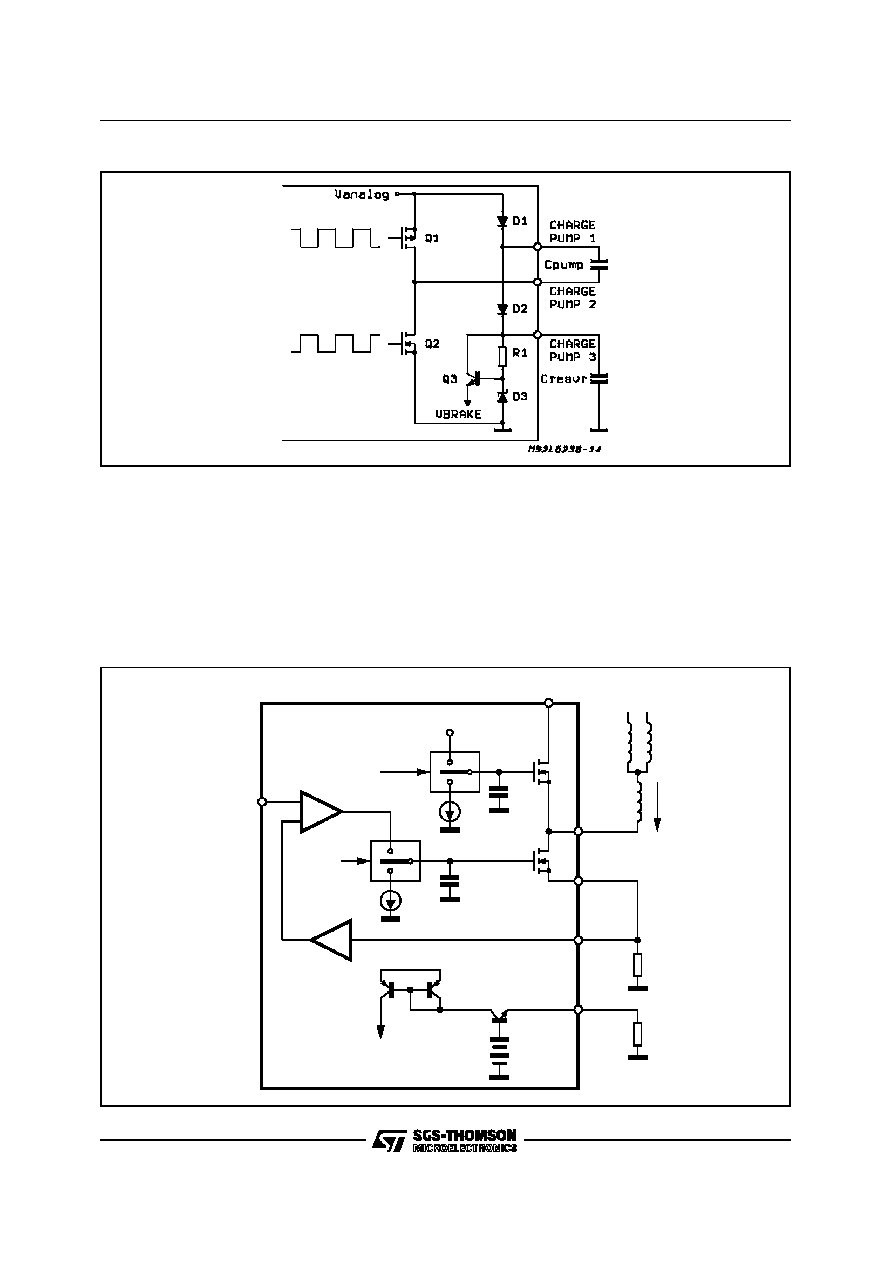
4.3 Charge Pump
The charge pump circuitry is used as a means of
doubling the analog supply voltage in order to al-
low the upper N-channel DMOS transistors to be
driven like P-channel devices. The energy stored
in the reservoir capacitor is also used to drive the
lower drivers in a brake mode if the analog supply
is lost. Figure 4-3 is a simplified schematioc of the
charge pump circuitry.
A capacitor, C
pump
, is used to retrieve energy
from the analog supply and then "pumps" it into
the storage capacitor, C
resvr
.
An internal 300KHz oscillator first turns ON Q2 to
quickly charge C
pump
to approximately the rail
voltage. The oscillator then turns ON Q1 while
turning OFF Q2. Since the bottom plate of C
pump
,
is now effectively at the rail voltage via D2.
A zener-referenced series-pass regulator supplies
Figure 4-3
I1
Islew
V
PUMP
SW2
1
0
Cfet
UPPER A
+
-
A2
VCTRL
X4
A3
VPOWER
I2
Islew
SW3
1
0
Cfet
OUTPUT
B
C
OUTA
L1
L2
L3
Q1
Q2
R
S
3.1V
SLEW RATE
REFERENCE CURRENT
Q3
Q4
Q5
R
SLW
RSENSE
CSA
PWM SLEW/RC
LOWER A
D95IN315
VANALOG
Figure 4-4
L6238S
17/31

a voltage, V
brake
, during brake mode.
The maximum capacitance specified for the Stor-
age Capacitor is 4.7
µ
F.For applications requiring
a larger value, an external diode should be con-
nected between Vanalog and the
Storage Ca-
pacitor to prevent excessive inrush current from
damaging the charge pump circuitry. A small
value resistor (i.e. 50W) may instead be inserted
in series with the Storage Capacitor to limit the in-
rush current.
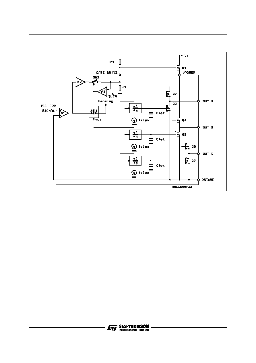
4.4 Linear Motor Current Control
The output current is controlled in a linear fashion
via a transconductance loop. Referring to Figure
4-4 the sourcing FET of one phase is forced into
full conduction by connecting the gate to V
pump
,
while the sinking transistor of an appropriate
phase operates as a transconductance element.
To understand the current control loop, it will be
assumed that Q2 in figure 4-4 is enabled via SW3
by the sequencer. During a run condition, the cur-
rent in Q2 is monitored by a resistor R
s
connected
to the R
sense
input.
The resulting voltage that appears across R
s
is
amplified by a factor of four by A3 and is sent to
A2 where it is compared to the Current Command
Signal. A2 provides sufficient drive to Q2 in order
to maintain the motor speed at the proper level as
commanded by the Speed Controller.
4.5 Transconductance Loop Stability
The RC network connected to the Compensation
pin provides for a single pole/zero compensation
scheme. The pole/zero compensation scheme.
The pole/zero locations are adjusted such that a
few dB of gain (typ. 20dB) remains in the tran-
sconductance loop at frequencies higher than the
zero.
The inductive characteristic of the load provides
the pole necessary for loop stability. Thus the
loop bandwidth is actually limited by the motor it-
self.
Figure 4-5 shows the complete transconductance
loop including compensation, plus the response.
The Bode plot depicts the normal way to achieve
stability in the loop. The pole andzero are used to
set a gain of 20dB at a higher frequency and the
pole of the motor cuts the gain to achieve stabil-
ity.
Loop instability may be caused by two factors:
1)The motor pole is too close to the zero. Refer-
ring to figure 4.6, the zero is not able to dec-
rement the shift of phase, and when the effect
of the pole is present, the phase shift may
reach 180
∞
and the loop will oscillate. To rec-
tify this situation, the pole/zero must be
shifted at lower frequencies by increasing the
compensation capacitor.
Figure 4-5
Figure 4-6
Figure 4-7
L6238S
18/31
2)The motor capacitance, CM, itself can inter-
fere with the loop, creating double poles. If
the gain at higher frequencies is sufficiently
high, the double pole slope of 40dB/decade
can cause the phase shift to reach 180
∞
,
re sulting in oscillation.
Figure 4-8 is a Bode plot showing how to correct
this situation. The bold line indicates the response
with relatively high gain at the higher frequencies.
By leaving the pole unchanged and increasing the
zero, the response indicated by the dashed lines
can be achieved.
4.6 Slew Rate Control
A 3-phase motor appears as an inductive load to
the power supply. The power supply sees a dis-
turbance when one motor phase turns OFF and
another turns ON because the FET turn-OFF time
is much shorter than the L/R rise time. Abrupt
FET turn-OFF without a proper snubbing circuit
can even cause current recirculation back into the
supply.
However, the need for a snubber circuit can be
eliminated by controlling the turn-OFF time of the
FETs.
The rate at which the upper and lower drivers turn
OFF is programmable via an external resistor,
S
slew
connected to the SLEW RATE pin. This re-
sistor defines an internal current source that is
utilized to limit the voltage slew rate at the outputs
during transition, thus minimizing the load change
that the power supply sees.
To insure proper operation the range of resistor
values indicated should not be exceeded and in
some applications values near the end points
should be avoided as discussed below.
Low Values of Rslew - If a relatively low value of
Rslew is selected, the resultant fast slew rate will
result in increased commutation cross-over cur-
rent, higher EMI, and large amount of commuta-
tion current.
This last case can cause voltage spikes at the
output that can go as much as lV below ground
level. This situation must be avoided in this inte-
grated circuit (as in most) since it causes unpre-
dictable operation.
High Values of Rslew - Higher values of Rslew
result of course in slow slew rates at the outputs
which is, under most conditions, the desired case
since the problems associated with fast rates are
reduced. The additional advantage is lower
acoustical noise.
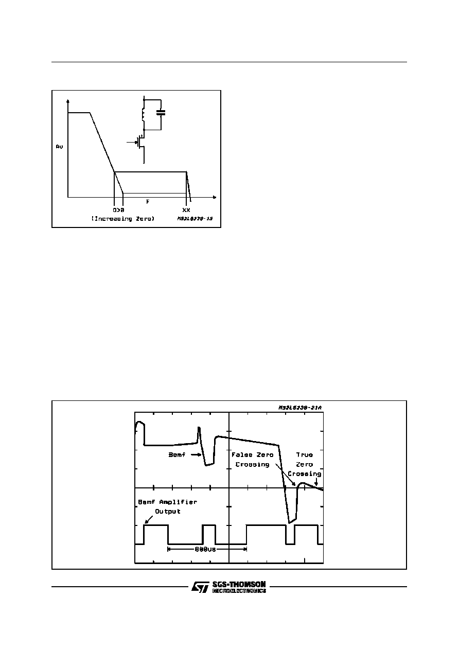
Problems can occur though if the slew rate for a
Figure 4-8
Figure 4-9: Effect of Slow Slew Rate.
L6238S
19/31
given application is too slow. Figure 4-9 is an os-
cillograph taken on a device that had a fairly large
value for Rslew and failed to spin up and phase
lock a motor.
The problem manifests itself as the motor begins
to spin up. At lower RPMs, the Bemf of the motor
is relatively small resulting in higher amounts of
commutation current. In figure 4-9, the upper
waveform is the voltage appearing at OUTPUT
relative to the CENTER TAP input. The lower
waveform is the actual output of the Bemf ampli-
fier available on special engineering prototypes.
The oscillograph was taken just as the problem
occured. The period between zero crossings was
~800
µ
s resulting in a mask time period of 200
µ
s.
As can be seen, the excessively long slew rate
actually exceeded the mask period and was de-
tected as a zero crossing.
This resulted in improper sequencing of the out-
puts relative to the proper phases and caused the
motor to spin down.
4.7 Ext PFET Driver
The power handling capabilities of the 3 phase
output stage can be extended with the addition of
a single P-Channel FET.
Figure 4-10 shows the Ext FET connection and
demonstrates how the L6238S automatically
senses the FETs presence. When the voltage at
the Gate Drive pin is
0.7V, the output of com-
parator A3 goes high, removing the variable drive
A1 from the internal FETs and connects them in-
stead to Vanalog via the commutation switches to
facilitate full conduction.
The upper FETs drive paths are not shown for
clarity. A3 also closes SW2 allowing A1 to linearly
drive the external P-Channel FET Q1 via inverter
A2.
4.8 Bemf Ampolifier
Since no Hall Effect Sensors are required, the
commutation information is derived from the Bemf
voltage zero-crossings of the undriven phase with
respect to the center tap. The Bemf comparator
and associated signal levels are depicted in figure
4-11. For reliable operation, the Bemf signal am-
plitude should be a minimum of
±
60 mV to be
properly detected. In order to provide for noise
immunity, internal hysteresis is incorporated in
the detection circuitry to prevent false zero cross-
ing detection.
For laboratory evaluation purposes, a simple re-
Figure 4-10: External P-Fet.
L6238S
20/31
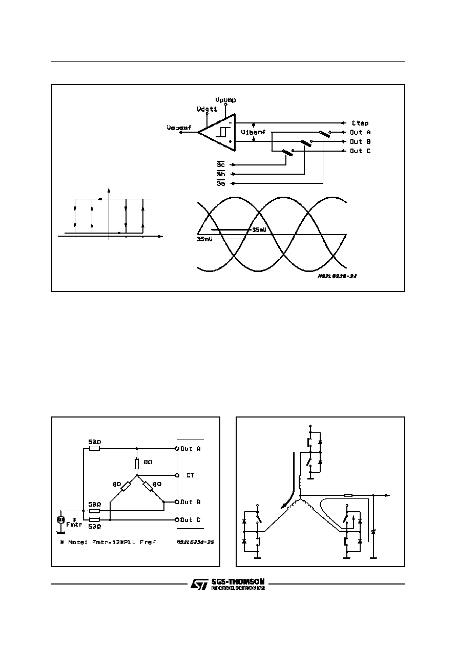
sistive network as shown in figure 4.12 can be
used to emulate the Bemf of the motor.
The actual Bemf zero-crossing is 30 electrical de-
grees (50% of a commutation interval) away from
the optimal switch point. A digital counter circuit
measures 50% of the previous interval to deter-
mine the next interval's commutation delay from
the zero crossing. During the low RPM stages of
start up the long commutation intervals may
cause the counter to overflow, in which case 50%
of the max count will be less than 50% of the
ideal commutation interval. Therefore, the torque
will not be optimal until the desired commutation
interval is less than the dynamic range of the
counter.
4.9 Center Tap Protection
Spindle Motors with a high number of windings
exhibit a transformer coupling effect that in some
cases can cause relatively high currents to flow
through the center tap input.
Current flowing out of the center tap pin as high
as 25mA has been observed with certain motors.
Figure 4-12: Bemf Emulator
R1 1K
DS1
TO CENTER
TAP INPUT
D95IN317
Figure 4-13
Figure 4-11: Bemf Amplifier.
Vo
BEMF
-35
-25
0
25
35
Vi
BEMF(mV)
SLOPE=0
SLOPE=1
D95IN316
L6238S
21/31

The high current flows from the grounded sub-
strate of the integrated circuit (p-type material),
through one or more epitaxial pockets (n-type ma-
terial) and out the center par pin.
This current can cause adverse operation of the
controllet due to substrate injection and might
possibility damage the internal metalization runs.
The normal current for this input is in the 200
µ
A
range.
Referring to figure 4-13, a simple protection
scheme consisting of a 1K resistor and a low cur-
rent Schottky diode should be added if the appli-
cation causes excessive current (i.e. >1mA) to
flow through the center tap pin.
5.0 PWM MOTOR CURRENT CONTROL
A unique feature of the L6238S in the optional
Pulse Width Modulation (PWM) control of motor
current.
Using Variable-frequency, Constant-OFF time
Current-Mode control, the L6238S can drive
higher power motors without the need for external
drivers, while minimizing internal power dissipa-
tion.
Additional benefits include reduced power supply
consumption (up to 50% savings) and lower watt-
age requirements for the current sensing resistor.
Constant-OFF time Current-Mode control, oper-
ates on the principle of monitoring the motor cur-
rent and comparison it to a reference or control
level.
When the motor current reaches this commanded
level, the output drivers turn OFF and remain
OFF for a Constant-OFF time. After this OFF time
the drivers turn back ON to repeat the cycle.
Figure 5.1 is a block diagram of the PWM control
circuitry. When using PWM as opposed to linear
control, two changes are made to the control
loop:
1.The slew rate control is disabled, allowing the
outputs to slew at a minimum rate of 10V/
µ
s.
This is accomplished by closing SW3 and
SW5.
2.The OTA amplifier is taken out of the control
loop via SW6. The lower drivers are now
driven into hard conduction by tying the gates
to the analog supply during the On time of the
PWM cycle.
The current in the motor windings is monitored via
the voltage dropped in the sensing resistor,
R
sense
.
This voltage is multiplied by a factor of 4 in the
Current Sense Amplifier (CSA) and sent to nega-
tive input of the PWM Comparator (A2).
The control voltage, V
control
, is applied to the posi-
tive input of A2. When the output of the CSA
reaches a level that is equal to the commanded
level, the output of A2 switches low, toggling the
latch comprised of N1 and N2. This causes the
upper drivers to turn off and opens SW1. Q3 turns
OFF allowing the Constant-OFF time capacitors,
I1
Islew
V
PUMP
SW2
1
0
Cfet
UPPER A
+
-
A1
PWM/SLEW
X4
A3
VPOWER
I2
Islew
SW3
1
0
Cfet
OUTPUT
B
C
OUTA
L1
L2
L3
Q4
Q5
SLEW RATE
REFERENCE
CURRENT
R
SLW
RSENSE
CSA
VCTRL
LOWER A
D95IN318
N3
Q1
Q2
VANALOG
3.1V
SW1
Q3
1.2V
SW5
N1
SW4
N2
A2
+
-
PWM/LIN
CONTROL
1
0
FROM TRANS. LOOP
CSA
SW6
V
ANALOG
COFF
RSLEW
Figure 5-1
L6238S
22/31

C
off
to discharge to dischargte through R
slew
, initi-
ating the Constant-OFF time-out. When the volt-
age on C
off
reaches 1.2V, comparator A1switches
state toggling the latch in the opposite state, turn-
ing the upper driver back ON. SW1 also closed
quickly charging up C
off
for the next cycle.
5.1 PWM Design Considerations
In order to select the parameters associated with
PWM operation, the following factors must be
taken into consideration:
1. PWM Switching Frequency
2. Duty Cycle
3. Motor Currents
4. Minimum ON Time
5. Noise Blanking
6. Bemf Masking/Sampling
5.1.1. PWM Switching Frequency
The PWM switching frequency F
pwm
is found
from:
F
pwm
=
1
T
on
+
T
off
(5.1.1)
where:
T
on
= The time required for the motor current
to reach the commanded level.
T
off
= The programmed OFF time.
The two main considerations for this parameter
are the minimum and maximum switching fre-
quency.
The maximum switching frequency occurs during
the Start-up and should be kept below 50KHz due
tointentional bandwidth limitations and output
switching losses.
5.1.2 Duty Cycle
Besides reducing the power dissipation of the
controller output stage, running in PWM offers 2
additional "free" benefits:
A. Reduced Powe Supply Current at Start Up
B. Lower Power Rating for the Motor Current
Sense Resistor.
Figure 5-2 is the current path during the ON time
of a phase period. The current from the supply
passes through the upper sourcing DMOS, Q3
transistor through the two driven winding, the
lower DMOS, Q2 and finally through the current
sensing resistor R
sns
. Since both Q3 and Q4 are
ON, while Q3 is turned OFF. The voltage, causing
the current to continue to flow through Q2, and
Q4.
If the duty cycle is nearor at 50%, then for 1/2 the
PWM cycle, no current is flowing from the power
supply or the sense resistor while current is still
flowing in the motor. This lowers the requirement
for both the Power Supply and the Power Rating
for the sensing resistor.
5.1.3 Motor Currents
Note: It is not the objective of this section to describe the principles
of brushless DC motor, but to provide sufficient information about the
parameters associated with PWM operation in order to optimize an
application.
A simplified model of a motor is shown in figure 5-
4. For this discussion, lower order effects due to
mutual inductance between windings, resistance
due to losses in the magnetic circuit, etc. are not
shown.
The motor at stall is equal to a resistance, Rmtr,
in series with an inductance, Lmtr. When the mo-
tor is rotating, there is an induced emf that ap-
pears across the armaure terminals and is shown
in figure 5-4 as an internally generated voltage
Ibemf), Eg.
L1
L2
OUTPUTA
OUTPUTB
D2
D1
D4
D3
Q1
Q2
Q3
Q4
V
POWER
R
SENSE
R
SNS
D95IN319
Figure 5-2
L1
L2
OUTPUTA
OUTPUTB
D2
D1
D4
D3
Q1
Q2
Q3
Q4
V
POWER
R
SENSE
R
SNS
D95IN320
Figure 5-3
L6238S
23/31
The relation between these variables is given by:
V
=
L
mtr
di
mtr
dt
R
mtr
i
mtr
+
E
g
(5.1.2)
where:
V
=
Applied Voltage
i
mtr
=
Motor Current
L
mtr
=
Total
inductance
of
the
motor
windings
R
mtr
=
Resistance in series with the motor
E
g
=
The internally generated voltage of
the motor, proportional to the motor
velocity
Since:
E
g
= K
E
(5.1.3)
The above equations can be combined to form
the basic electrical equation for a motor:
V
=
L
mtr
di
mtr
dt
R
mtr
i
mtr
+
K
E
(5.1.4)
Figure 5.5 is a simplified electrical equivalent of
the output stage of the L6238S along with the
model of the motor during the time that the Out-
put Drives are conducting.
The additional resistance associated with the out-
put stage and sensing resistor are also in series
with the motor. If we let R
s
equal the total series
resistence:
R
s
= 2*R
dsON
+ R
mtr
+ R
sense
(5.1.5)
then (5.1.4) becomes:
V
=
L
mtr
di
mtr
dt
R
s
i
mtr
+
E
g
(5.1.6)
Figure 5-6 is an equivalent circuit of the output
stage during the Constant-OFF period. During the
OFF time the lower driver for the particular phase
beign driven remains ON.
The internally generated voltage forces the path
of current though the motor, its series resistance,
the RdsON of the Lower Driver and finally through
the opposite lower driver.
PWM Example (Refer to Figure 5-7)
The following is an example on how to select the
timing parameters.
Given:
DCStart Current
=
1.25A
Ripple Current
=
100mA
Duty Cycle
=
50%
Motor Interface (L)
=
880
µ
H
Total Series Resistance (R
s
)
=
4.8
If the worst case start current is 1.25A and the
duty cycle is 50%, then the Peak Current, It will
be:
i
t
=
1.25
+
0.1
2
i
t
= 1.30A
Eg
+
-
Rmtr
Lmtr
D95IN321
Figure 5-4
+
-
Rmtr
Lmtr
D95IN322
UPPER
Rdson
KEW
LOWER
Rdson
Rsense
Figure 5-5
+
-
Rmtr
Lmtr
D95IN323
KEW
LOWER
Rdson
LOWER
Rdson
Figure 5-6
L6238S
24/31

The Valley current, I
b
will thereforebe:
i
b
= 1.30 - 0.1A
i
b
= 1.20A
During the Align and Go Phase (where the power
dissipation requirements are highest, Eg is zero.
The initial time required to reach the Peak current
is:
t
init
= ±
L
R
ln
1
±
I,R
V
(5.1.7)
Substituting values:
t
init
= ±
880e
±
6
4.8
ln
1
±
1.3
4.8
12
t
init
= 134.6
µ
s
The ON time can be calculated from:
t
on
=
L
R
s
ln
V
R
s
±
i
b
V
R
s
±
i
t
(5.1.8)
Substituting values:
t
on
=
880E
±
6
4.8
ln
12
4.8
±
1.2
12
4.8
±
1.3
t
on
= 14.67
µ
s
During the OFF time, the motor current continues
to flow through the DMOS transistors and threfore
the voltage drop remains constant across the
windings.
The time required for the inductor current to reach
the valley current is given by:
t
off
=
L
R
ln
I
t
I
b
(5.1.9)
Substituting values:
t
off
=
880e
±
6
4.8
ln
1.3
1.2
t
off
= 14.67
µ
s
Note: that the parameters for this example were selected to arrive at
a 50% duty cycle. This will not always be the case due to factors such
as fixed motor parameters, etc.
The Constant Off timer period can be determined
from:
t
off
=
R
slew
C
off
ln
V
chrg
V
trip
(5.1.10)
Where:
T
off
=
Constant-OFF Time
R
slew
=
Slew Rate Resistor
C
off
=
Off Time Capacitor
V
chrg
=
Initial Capacitor Charge Voltage
V
trip
=
Capacitor Lower Trip Threshold
Substituting nominal values given:
T
off
= 0.75
R
slew
C
off
Solving for C
off
C
off
=
T
off
0.75R
slew
In the example, to set the OFF timer for a 50%
duty cycle:
Given:
T
off
=
14.67
µ
s
R
slew
=
100K
(typical Value)
C
off
=
14.67e
±
6
100e
3
C
off
146pF
5.1.4 Minimum ON Time
The bandwidth of the PWM loop was optimized to
reject unwanted switching noise while providing
20
µ
s/DIV
Iout A
200mA
D95IN324
4
It=1.3A
Ib=1.2A
Iavg=1.25A
Figure 5-7
L6238S
25/31
sufficient response, commensurate with
the
switching speed of the output drivers. At higher
frequencies the switching losses inherent in the
drivers start to negative any of the power dissipa-
tion savings gained with PWM operation.
The current sense amplifier has a minimum slew
rate of 0.31V/
µ
s. With a worst case Motor peak
start-up current of 2.5A and Sense Resistor of
0.33, the resultant R
sense
voltage would be equal
to 825mV. With a minimum gain of 3.8V/V, the
CSA output voltage would have to slew to 3.14V.
Therefore it would require approximately 10
µ
s for
the output voltage to reach the required com-
manded level.
If an ON time were selected that was less than
this time, the motor current would overshoot the
desired level resulting in incorrect current control
possibly exceeding the output capabilities of the
drivers.
5.1.5 Noise Blanking
Referring to Figure 5-8, when operating with
lower levels of current (i.e. < 700mA, with Rsense
= 0.33
), the possibility exiss where the noise
due to output Turn-ON can exceed the Com-
manded Current Level causing prematire Turn-
OFF.
In order to provide noise immunity from this
switching noise, a blanking circuit automatically
rejects any signal appearing at the output of the
CSA for a 3
µ
s period.
Figure 5-9 is an additional block diagram of the
PWM control loop including the noise blanking cir-
cuit. The output of A3 goes high when ever the
voltage at the CSA input is more positive then the
Control Voltage.
This is the case when either the motor current or
the turn-ON transient has reached the com-
manded level. The output of A3 is gates by N11.
In order to provide a blanking period, Q1 is turned
10
µ
s/DIV
Vrsense
D95IN325
1
3
µ
s BLANKING PULSE
COMMANDED
CURRENT LEVEL
Figure 5-8
C1
8pF
Q1
N6
N10
I1
5
µ
A
N1
DELAY
TO OUPUT
DRIVERS
N7
N8
N11
N9
N12
2.4V
SW1
A2
+
-
1.2V
A3
+
-
N4
N2
N3
CLK_BEMF
N5
I2
20
µ
A
Q2
X4
PWM/LIN
RUN/BRAKE
N12
Q3
PWM TIMER
C4
PWM COMP
VCONTROL
CSA INPUT
PWM_SLEW
C3
R1
D95IN326
Figure 5-9
L6238S
26/31

ON during the Constant-OFF time, charging C1 to
the internal rail. At the end of the OFF time, Q1 is
turned OFF allowing current source I1 to dis-
charge the capacitor towards ground. While the
voltage on C1 is above the low input threshold of
N1, the output of N1 is low, preventing any
change of state at the output of N11 due to a high
A3 output. When the capacitor reaches the low in-
put threshold of N1, N1 chnges state allowing A3
to control the state of N11.
5.1.6 Masking/Bemf Sampling in PWM
The method of sampling the floating phase for the
bemf zero crossing defers between Linear and
PWM operation. In Linear Mode, the bemf is sam-
pled continuously after the mask time-out, until
the zero crossing is detected. Then the mask is
enabled for a time based on the commutation
phase delay plus the additional time based on the
previous period as explained earlier.
With PWM operation however, the switching
noise at turn ON (after the Constant-OFF time)
can be significant, especially at low RPMs where
the bemf is the lowest. In order to provide the
greatest noise immunity in PWM, the floating
phase is monitored only at the point where the
output is about to be turned OFF.
In operation, when the motor current reaches the
commanded level, the floating phase is first moni-
tored to determine if the bemf has crossed the
zero. The output is then turned OFF for the Con-
stant-OFF time out.
As the motor current increases through, the in-
creasing bemf causes the motor current to natu-
rally decrease. Eventually a point is reached
where the PWM is running at 100% duty cycle
and the motor current cannot reach the com-
manded level. At this time the bemf is no longer
smpled, preventing further commutation of the
output.
The PWM Limit Timer is used to set up a maxi-
mum ON time. When this limit is exceeded the
method of sensing the bemf is essentially the
same as in the case of operating in linear mode.
Figure 5-10 is an oscillograph of the controller op-
erating in PWM mode. The top trace is A
out
. The
2nd trace is the voltage seen at the PWM/SLEW
pin indicating the exponential discharging of the
timing capacitor during the OFF time. Trace 3 is
the voltage appearing on the PWM Timer capaci-
tor, while trace 4 is the motor current.
Referring again to Figure 5-9, and 5-10 transistor
Q2 is turned ON at the beginning of the OFF time,
discharging the external capacitor C4 to near
ground level. At the end of the OFF-Time, Q2 is
turned off and C4 starts charging linearly via I2.
C4 is again discharged at the beginning of the
OFF time and the cycle repeats. As long as C4
does not reach the threshold of A1 (typically
3.5V), the bemf is only sampled just before turn-
off of the output. As the motor is starting up in fig-
ure 5-10, the duty cycle is roughly 50%. The
PWM limit timer is reset to ground by the start of
the OFF timer before reaching the 3.5V threshold.
In figure 5-11, as the motor spins up, the on time
of the output increases and the PWM limit timer
reaches the 3.5V. Eventually the duty cycle
reaches 100% and the sampling of the bemf is
essentially the same as in the linear mode.
The selection of components for the PWM timer is
not critical. Since the objective is to sample the
bemf only at turn OFF to maximize the signal to
noise ratio, the PWM timer slope can be set up to
convert to the full bemf sampling after a few revo-
lutions of the motor when the bemf has reached
an appropriate voltage output.
20
µ
s/DIV
4
1A
Iout A
Aout
D95IN327
Fpwm=50KHz
Coff=120pF
Ctmr=220pF
3
500mV
2
2V
PWM/Slew
1
10v
PWM Limit
Timer
Figure 5-10
50
µ
s/DIV
4
Aout
Iout A
D95IN328
Fpwm=12KHz
Coff=120pF
Ctmr=220pF
3
500mV
2
2V
PWM/Slew
1
10V
PWM Limit
Timer
1A
Figure 5-11
L6238S
27/31

PLCC44 PACKAGE MECHANICAL DATA
DIM.
mm
inch
MIN.
TYP.
MAX.
MIN.
TYP.
MAX.
A
17.4
17.65
0.685
0.695
B
16.51
16.65
0.650
0.656
C
3.65
3.7
0.144
0.146
D
4.2
4.57
0.165
0.180
d1
2.59
2.74
0.102
0.108
d2
0.68
0.027
E
14.99
16
0.590
0.630
e
1.27
0.050
e3
12.7
0.500
F
0.46
0.018
F1
0.71
0.028
G
0.101
0.004
M
1.16
0.046
M1
1.14
0.045
L6238S
28/31

A
A2
A1
B
Seating Plane
C
11
12
22
23
33
34
44
E3
D3
E1
E
D1
D
e
1
K
B
PQFP44
L
L1
0.10mm
.004
PQFP44 PACKAGE MECHANICAL DATA
DIM.
mm
inch
MIN.
TYP.
MAX.
MIN.
TYP.
MAX.
A
3.40
0.134
A1
0.25
0.010
A2
2.55
2.80
3.05
0.100
0.110
0.120
B
0.35
0.50
0.0138
0.0197
C
0.13
0.23
0.005
0.009
D
16.95
17.20
17.45
0.667
0.677
0.687
D1
13.90
14.00
14.10
0.547
0.551
0.555
D3
10.00
0.394
e
1.00
0.039
E
16.95
17.20
17.45
0.667
0.677
0.687
E1
13.90
14.00
14.10
0.547
0.551
0.555
E3
10.00
0.394
L
0.65
0.80
0.95
0.026
0.0315
0.0374
L1
1.60
0.063
K
0∞
(min.), 7
∞
(max.)
L6238S
29/31
A
A2
A1
B
C
16
17
32
33
48
49
64
E3
D3
E1
E
D1
D
e
1
K
B
TQFP64
L
L1
Seating Plane
0.10mm
TQFP64 PACKAGE MECHANICAL DATA
DIM.
mm
inch
MIN.
TYP.
MAX.
MIN.
TYP.
MAX.
A
1.60
0.063
A1
0.05
0.15
0.002
0.006
A2
1.35
1.40
1.45
0.053
0.055
0.057
B
0.18
0.23
0.28
0.007
0.009
0.011
C
0.12
0.16
0.20
0.0047
0.0063
0.0079
D
12.00
0.472
D1
10.00
0.394
D3
7.50
0.295
e
0.50
0.0197
E
12.00
0.472
E1
10.00
0.394
E3
7.50
0.295
L
0.40
0.60
0.75
0.0157
0.0236
0.0295
L1
1.00
0.0393
K
0∞
(min.), 7
∞
(max.)
L6238S
30/31

Information furnished is believed to be accurate and reliable. However, SGS-THOMSON Microelectronics assumes no responsibility for the
consequences of use of such information nor for any infringement of patents or other rights of third parties which may result from its use. No
license is granted by implication or otherwise under any patent or patent rights of SGS-THOMSON Microelectronics. Specification mentioned
in this publication are subject to change without notice. This publication supersedes and replaces all information previously supplied. SGS-
THOMSON Microelectronics products are not authorized for use as critical components in life support devices or systems without express
written approval of SGS-THOMSON Microelectronics.
©
1995 SGS-THOMSON Microelectronics ≠ Printed in Italy ≠ All Rights Reserved
SGS-THOMSON Microelectronics GROUP OF COMPANIES
Australia - Brazil - Canada - China - France - Germany - Hong Kong - Italy - Japan - Korea - Malaysia - Malta - Morocco - The Netherlands -
Singapore - Spain - Sweden - Switzerland - Taiwan - Thailand - United Kingdom - U.S.A.
L6238S
31/31