 | –≠–ª–µ–∫—Ç—Ä–æ–Ω–Ω—ã–π –∫–æ–º–ø–æ–Ω–µ–Ω—Ç: L6246ES4 | –°–∫–∞—á–∞—Ç—å:  PDF PDF  ZIP ZIP |
L6246
12V VOICE COIL MOTOR DRIVER
12V (
±
10%) OPERATION
3A MAXIMUM CURRENT CAPABILITY
0.3
MAXIMUM ON RESISTANCE OF EACH
POWER DMOS AT A JUNCTION TEM-
PERATAURE OF 25∞C
CLASS AB POWER AMPLIFIERS
LOGIC AND POWER SUPPLY MONITOR
POWER ON RESET
PARKING FUNCTION WITH SELECTABLE
RETRACT VOLTAGE AND DYNAMIC BRAKE
BEFORE PARKING
ENABLE FUNCTION
GATE DRIVER FOR EXTERNAL BLOCKING
N-MOSFET
OVERTEMPERATURE PROTECTION
OVERTEMPERATURE WARNING OUTPUT
PQFP44 PACKAGE
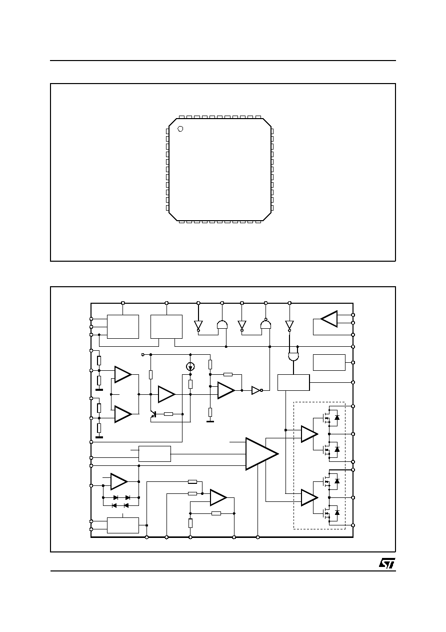
DESCRIPTION
The voice coil driver L6246 is a linear power am-
plifier designed to drive single phase bipolar DC
motors for hard disk drive applications. The de-
vice contains a selectable transconductance loop,
which allows high precision for head positioning.
The power stage is composed of 2 power amplifi-
ers, in AB class, with 4 DMOSs, with Rdson of
0.5
(Sink+Source) maximum, in a H-bridge con-
figuration. Drive voltage for the upper DMOS
FETs is provided by a charge pump circuit to en-
sure low Rdson.
Automatic brake and parking of the head actuator
is performed by logic or when a failure condition
is detected by power supply monitors. An external
resistor programs the parking voltage that en-
ables the head retract. In addition, a 5V stable
output is provided for the external usage, and a
gate driver circuit enables an external power sup-
ply isolation N-MOSFET.
This device is built in BCD II technology allowing
dense digital circuitry to be combined with high
power bipolar power devices and is assembled in
PQFP44.
August 2003
Æ
PQFP44 (10x10)
MULTIPOWER BCD TECHNOLOGY
1/12
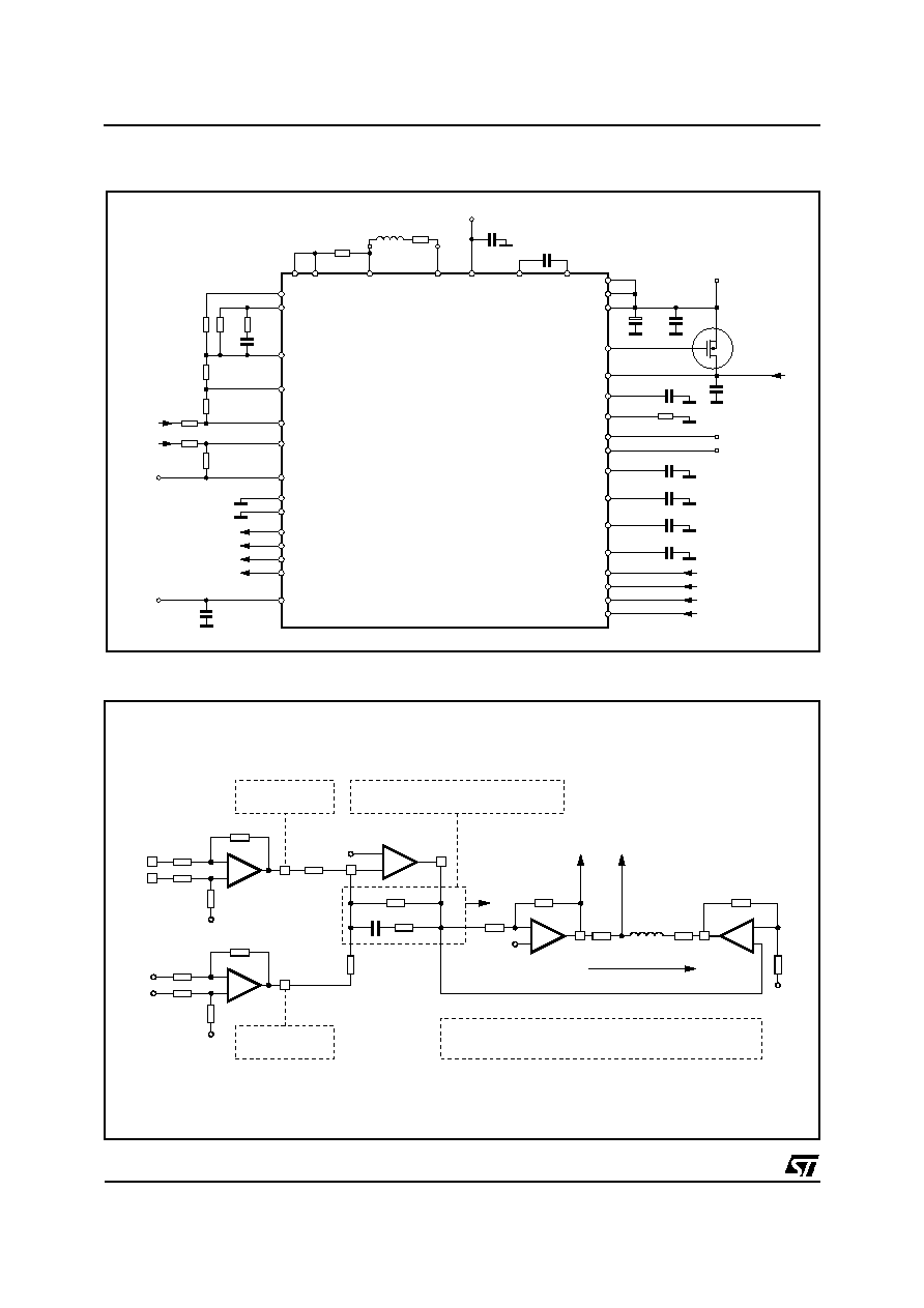
CHARGE
PUMP
GATE
DRIVER
CP_GND
GATE DRIVE
-SPINDLE
START
MOTOR
START -W_GATE
-AE
W_GATE
VCM
PARK
C1
C2
VCP
THERMAL
-THERMAL SD
V
CC
+12
FILTER CAP
+
-
+
-
REF1
V
DD
+5
FILTER CAP
PARKING
RPARK
REF1
VPARK
10K
10K
+5
4
µ
A
10K
30K
25K
20K
V
CC/2
ERR_OUT
BRAKE
CIRCUIT
+
-
+
-
+
-
+
-
V
CC/2
ERROR
AMPL.
+
-
VBEMF
REF. VOLT.
GENERATOR
SENSE
AMPLIFIER
SENSE_
OUT
SENSE
_IN-
SENSE
_IN+
V
CC/2
ERR-
+5V REF
+5V REF_GND
REF1
INPUT
AMPLIFIER
VIN-
VIN+
VIN_OUT
-POR
BRAKE DELAY
V
CC
OUT+
GND
V
CC
OUT-
GND
D95IN242B
POWER AMPLIFIERS
T_CAP
+
-
BLOCK DIAGRAM
1
2
3
5
6
4
7
8
9
10
17
11
18 19 20 21 22
44 43 42 41
39
40
38 37 36 35 34
28
27
26
24
23
25
33
32
31
29
30
SENSE-IN-
SENSE-IN+
-THERMAL SD
FILTER_CAP
N.C.
BRAKE DELAY
N.C.
SENSE-OUT
ERR-
GND
ERR-OUT
VIN_OUT
VIN-
VIN+
V
CC/2
-AE_W_GATE
MOTOR START
V
DD
V
CC
-POR
+5V REF
T_CAP
GATE DRIVE
GND
OUT-
V
CC
C2
VCP
C1
V
CC
OUT+
GND
CPGND
RPARK
VBEMF
+12SETPT
+5V REF_GND
N.C.
+5SETPT
N.C.
ENABLE
-SPINDLE START
-W_GATE
VCM PARK
D95IN241B
12 13 14 15 16
PIN CONNECTION (Top view)
L6246
2/12
ABSOLUTE MAXIMUM RATINGS
Symbol
Parameter
Value
Unit
V
pow. max.
Maximum supply voltage
15
V
V
digital max.
Maximum supply voltage
7
V
V
in max.
Maximum input voltage
V
digital
±
0.3
V
V
in min.
Minimum input voltage
GND - 0.3
V
I
peak
Peak sink/source output current
3
A
I
dc
DC sink/source output current
1.7
A
P
tot
Maximum total power dissipation
1.7
W
T
op
Operative temperature range
0 to 80
∞C
THERMAL DATA
Symbol
Parameter
Value
Unit
R
th j-case
Thermal resistance junction to case
20
∞C/W
R
th j-amb
Thermal resistance junction to ambient mounted on standard PCB (*)
66
∞C/W
R
th j-amb
Thermal resistance junction to ambient mounted on PCB (**)
35
∞C/W
(*) Standard board construction: single layer (1S 0P); size 100mm long by 100mm wide.
(**) The board construction includes: a 6 layer board (2S 4P, with power planes
80%); size 136mm long by 99mm wide; package location
near middle point of lenght and one third of width.
PIN FUNCTIONS
Pin
Name
Description
1
N.C.
Not Connected.
2
Filter_cap
Filter capacitor for 10V internal regulator. The capacitor is optional.
3
Brake Delay
Voice Coil Motor brake delay capacitor.
4
-Thermal SD
Pre Thermal Shut Down indication Output.
5
Sense_in+
Non inverting Input of Sense Amplifier.
6
Sense_in-
Inverting Input of Sense Amplifier.
7
Gnd
Ground.
8
Err_out
Error Amplifier Output.
9
Err-
Inverting Input of Error Amplifier.
10
Sense_out
Output of Sense Amplifier.
11
N.C.
Not Connected.
12
Vin_out
Output of Input Amplifier.
13
Vin-
Inverting Input of Input Amplifier.
14
Vin+
Non inverting Input of Input Amplifier.
15
+Vcc/2
Half Supply Voltage reference.
16
+Motor start
Motor start Output to Spindle Controller.
17
-AE_W_Gate
Write Gate Output to AE.
18
+Vdd
+5V Supply.
19
+Vcc
+12V Supply.
20
-POR
Power On Reset. Low will signal the failure of the logic supply or 12V supply
21
+5V Ref
+5V Reference Output from the Voltage Reference Regulator.
22
T_cap
Power On Reset Timing Capacitor. The capacitor sets the POR delay.
23
N.C.
Not Connected.
24
+5V Ref Gnd
Ground for Voltage Reference Generator.
25
+5Setpt
+5V Monitor Set Point and filtering
L6246
3/12
ELECTRICAL CHARACTERISTICS (T
j
= 25∞C, Vdd = 5V, Vcc = 12V; unless otherwise specified.)
Symbol
Parameter
Test Condition
Min.
Typ.
Max.
Unit
Vcc
Analog/Power supply voltage
range
10.8
12
13.2
V
Vdd
Digital supply voltage range
4.5
5
5.5
V
Idd
Digital supply quiescent current
Output ENABLED
5
mA
Idd
Digital supply quiescent current
Output DISABLED
5
mA
Icc
Power supply quiescent current
Output ENABLED
20
mA
Icc
Power supply quiescent current
Output DISABLED
10
mA
THERMAL SHUT DOWN DATA
T
h_SD
Shut down Temperature
135
160
∞C
T
h_SD_H
Shut down hysteresys
25
∞C
T
h_Warn
Pre Shut down alarm
115
140
∞C
Pre Shut down alarm hysteresys
15
∞C
EXTERNAL N-MOSFET GATE DRIVER
Vll
Low level voltage
500
mV
Vhl
High level voltage
Vcc+4
V
Isink
Current sinking capability
4
mA
Isource
Current source capability
0.5
mA
POWER ON RESET AND GATE SPECIFICATION
V
dd_und_th
Digital undervoltage threshold
3.8
4.1
4.45
V
V
cc_und_th
Power undervoltage threshold
8.5
9.25
10.0
V
POR
_to
POR timeout
Cpor = 1
µ
F
375
500
625
ms
POR
_delay
Time delay for POR Active
1
µ
s
V
dd_POR_T_R
Power supply POR thereshold
Resistance
10
K
PIN FUNCTIONS (continued)
Pin
Name
Description
26
+12Setpt
+12V Monitor Set Point and filtering
27
Vbemf
Input BEMF from spindle motor for parking circuit.
28
Rpark
Resistor for setting the park voltage.
29
-W_Gate
Write Gate Input.
30
+VCM park
External input for parking. High will activate the park procedure.
31
-Spindle_start
Spindle Start input.
32
+Enable
Input. logic low will disable only the IC.
33
N.C.
Not Connected.
34
Cpgnd
Charge Pump Ground.
35
Gnd
Ground.
36
Out+
Power Amplifier Output.
37
Vcc
+12V Power Supply.
38
C1
Charge Pump Oscillator Output.
39
C2
Input for external Charge Pump Capacitor.
40
Vcp
Output for Charge Pump Storage Capacitor.
41
Vcc
+12V Power Supply.
42
Out-
Power Amplifier Output.
43
Gnd
Ground.
44
Gate Drive
Gate Drive for External Isolation N-MOSFETS.
L6246
4/12
ELECTRICAL CHARACTERISTICS (continued)
Symbol
Parameter
Test Condition
Min.
Typ.
Max.
Unit
V
CC_POR_T_R
Logic supply POR thereshold
Resistance
10
K
I
_POR_O
POR output current drive
4
mA
LOGIC INTERFACE VOLTAGE LEVEL (All digital inputs are CMOS compatible)
Voh
CMOS high level output voltage
Iout = 1.0mA
4.10
V
Vol
CMOS low level output voltage
Iout = 1.0mA
0.40
V
Vih
TTL high level input voltage
2
V
Vil
TTL low level input voltage
0.80
V
5V REFERENCE GENERATOR
Vref
Voltage reference at Power On
4.75
5.00
5.25
V
Drift
Drift from Power On
-2
+2
%
loref
Current output
10
mA
INPUT AMPLIFIER
Vi
Input voltage range
Vref (-)
Vref (+)
V
Vcm
Input common mode voltage
range
0
5.00
V
Vds
Input differential voltage swing
-5
+5
V
Vos
Input offset voltage
-5
+5
mV
Ib
Input Bias current
-500
+500
nA
Gv
Open Loop voltage Gain
80
dB
SR
Output slew rate
0.6
V/
µ
s
GBW
Gain bandwidth product
1
MHz
PSRR
Power supply rejection ratio
80
dB
Vo
Output voltage swing
9
V
ERROR AMPLIFIER
Vi
Input voltage range
V
CC
/2
-0.5
V
CC
/2
+0.5
V
Vos
Input offset voltage
-5
+5
mV
Ib
Input Bias current
-500
+500
nA
Gv
Open Loop voltage Gain
80
dB
SR
Output slew rate
0.6
V/
µ
s
GBW
Gain bandwidth product
1
MHz
PSRR
Power supply rejection ratio
80
dB
Vo
Output voltage swing
V
CC
/2
-2Vbe
V
CC
/2
+2Vbe
V
SENSE AMPLIFIER
Vi
Input voltage range
Gnd
Vcc
V
Vos
Input offset voltage
-6
+6
mV
Ii
Input sink and source current
-1.5
+1.5
mA
PSRR
Power supply rejection ratio
50
dB
Gv
Vloltage gain
9.9
10
10.1
V/V
Rin
Differential input resistance
3
K
GBW
Gain bandwidth product
1
MHz
Vli
Linear differential input voltage
range
Gv = 10(V/V)
-0.35
+0.55
V
CMRR
Common mode rejection ratio
56
dB
L6246
5/12
BLOCK DESCRIPTION
POWER AMPLIFIERS
The two power amplifiers are connected in bridge
configuration working in AB class.
SENSE AMPLIFIER
This stage senses the voltage drop across the
Rsense.
The input stage is supplied by the charge pump
voltage to have an high dynamic, while the other
sections of the amplifier are supplied by the volt-
age of 10.5V internally regulated to have an high
power supply rejection (this voltage, supplies also
the error amplifier, the input amplifier and the op-
erational amplifier which generates the Vcc/2 volt-
age).
The open loop gain is around 80dB and the band-
with is more than 1MHz.
The voltage gain is fixed internally at 10 V/V.
ERROR AMPLIFIER
This is the stage which compares the input volt-
age and the sense voltage, generating the control
voltage for the power section.
The open loop gain and bandwith of this amplifier
are similar to the sense amplifier.
The negative input and the output of the error am-
plifier are accessible externally in order to have
the current loop compensation user configurable.
The dynamic of the output is limited at +/- 2Vbe to
have a faster response of the output voltage.
INPUT AMPLIFIER
The inputs and the output pins are externally ac-
cessible to have the possibility to configure the
transconductance gain of the current control loop
selecting the voltage gain of this amplifier.
The open loop gain and bandwith of this amplifier
are similar to the sense amplifier.
REFERENCE VOLTAGE GENERATOR
This block generates the two reference voltage
Vcc/2 and +5VREF.
The Vcc/2 voltage is used as reference by the
current control loop.
The +5VREF is a very stable voltage generator
that can be used as reference voltage of an exter-
nal DAC.
ELECTRICAL CHARACTERISTICS (continued)
Symbol
Parameter
Test Condition
Min.
Typ.
Max.
Unit
POWER AMPLIFIER
Rdson
DMOS on resistance
at 25∞C
0.3
Gdv
Differential voltage gain
32
V/V
Iol
Output current leakage
500
µ
A
SR
Output slew rate
0.4
V/
µ
s
Tsr
Saturation recovery time
5
µ
s
GBW
Gain bandwidth product
100
KHz
RETRACT
Vr
Max. retract voltage
Vcc shorted to GND
300
mV
Vr
Max. retract voltage
Vcc Normal
1
V
CHARGE PUMP
Cs
Storage capacitor
1
µ
F
Vs
Storage voltage
Vcc +4
V
Cp
Pump capacitor
0.2
µ
F
RETRACT TRUTH TABLE
Input
Input
Output
Output
-Retract
+Enable
Bridge Enable
+Retract
Brake and Retract
0
X
0
1
Run
1
1
1
0
Disable
1
0
0
0
L6246
6/12

POWER SUPPLY MONITOR
This circuit monitors the logic supply (5V) and the
power supply (12V) and activates the power on
reset output (POR) and the VCM PARK circuit.
After both logic and power supply reach their
nominal value a timing capacitor (T_CAP) has to
be charge before the POR output change from
low to high level.
POR delay
=
C
V
I
where:
C is the capacitor value connected at pin
T_CAP
V is delta voltage that capacitor have to be
charged (2.3V)
I is the costant current charging the capacitor
(4
µ
A typ.)
At the two input pins, +12 FILTER CAP and + 5
FILTER CAP, can be connected two capacitors
for filtering the noise on the power supply, avoid-
ing in this case undesired commutations of the
POR signal because of some fast negative spikes
on the line.
BRAKE AND PARKING CIRCUITS
The voice coil driver is switched into the parking
condition through the VCM PARK input or when
the POR signal is low. In such condition immedi-
ately the output stage turns on the two lower
DMOS of the power bridge to activate the BRAKE
of the voice coil motor.
After a delay generated by the capacitor at the
BRAKE DELAY pin, only one of the two lower
DMOS stays on while the opposite half bridge is
tristated.
BRAKE delay
=
C
V
I
where:
C is the capacitor value connected at pin
BRAKE DELAY
V is delta voltage that capacitor have to be
charged (3V)
I is the costant current charging the capacitor
(5
µ
A typ.)
The parking voltage is then supplied by the
PARKING circuit connected to the output that has
been tristated.
The value of such a voltage is set by connecting
an external resistor between the RPARK pin and
ground.
V
r
=
Vbandgap
10
4
Rpark
where:
Vr is the retract voltage for parking the heads
Vbandgap is the internal bandgap reference
voltage of 1.4V
Rpark is value of the resistor connected at
RPARK pin
The parking circuit takes the power supply from
the spindle driver through the VBEMF pin, so that
in case of power fail the retract of the heads is
possible using the rectified BEMF voltage coming
from the spindle motor.
CHARGE PUMP
The charge pump circuit is used as a means of al-
most doubling the power supply voltage (12V) in
order to drive the upper DMOS of the power
bridge.
The energy stored in the in the capacitor con-
nected at VCP pin is also used to drive the gate
of the external N-MOSFET.
GATE DRIVER
This circuit provide the voltage driving the gate of
the external isolation N-MOSFET, and it is con-
trolled by the POR signal.
THERMAL
The thermal protection circuit has two threshold,
the first if the pre shut down alarm that activates
the THERMAL SD signal and the second is the
shut down temperature that tristates the output
stage when the junction temperature increases
over this level.
APPLICATION INFORMATION
Example of calculation of the error amplifier com-
pansation for the stability of the current control
loop. As can be seen from the draw of the current
control loop circuit of the next page, the voltage
across the load is:
#1
V
L
= A
CPW
A
CERR
(A
CINP
V
IN
- A
CENSE
V
sense
)
V
sense
= Rs
I
L
V
L
= ( Z
L
+ Rs)
I
L
where A
C
... is the closed loop gain of Power, Er-
ror, Sense and Input Amplifier.
Changing in the #1 the transfer function between
the load current and the V
IN
is:
#2
I
L
V
IN
=
A
CPW
A
CERR
A
CINP
Z
L
+
R
S
+
A
CPW
A
CERR
A
CSENSE
R
S
L6246
7/12
L6246
PQFP44
10
8
9
12
13
1K
100nF
ERR-
ERR_OUT
SENSE_OUT
1M
1K
1K
10K
VIN_OUT
VIN-
14
VIN+
10K
10K
10K
V
CC/2
V
REF
V
CTL
15
V
CC/2
34
7,35,43
CPGND
GND
Rs 0.2
LL
RL
VOICE COIL
MOTOR
OUT_
SENSE_IN-
SENSE_IN+
OUT+
42
6
5
36
V
DD
100nF
V
DD
18
22
µ
F
100nF
V
CC
V
CC
V
CC
V
CC
GATE DRV
19
41
37
44
27
G
S
D
V
BEMF
FROM SPINDLE
DRIVER
100nF
40
28
R
PARK
V
CP
P322
1
µ
F
51K
26
12S
EPT
(*)
25
5S
SEPT
(*)
10nF
C1
C2
38
39
21
5V
REF
24
5V
REF
GND
5V
REF
GND
22
12S
EPT
1
µ
F
3
5S
SEPT
1
µ
F
AE W GATE
MOTOR START
THERMAL SHTD
POR
17
16
4
20
32
ENABLE
30
VCM PARK
31
SPINDLE START
29
W GATE
2
FILTER_CAP
10.5V
INT.REG.
(*)
D95IN268
FILTER CAPACITORS TO BE SET IN APPLICATION
Typical Application Circuit
20K
2K
2K
V
CC/2
+ 10V
SENSE
20K
V
CC/2
V
CC/2
SENSE
AMPL.
R1
ERROR
AMPL.
-
+
RC (=R1)
V
CC/2
- (RA-RB) VIN
RA
RB
RB
RA
INPUT
AMPL.
-
+
R2
R3
C
VIN
V
SENSE
V
CC/2
17.5K
1.1K
V
CC/2
16.5K
V
CC/2
V
CC/2
+ (RA/RB) (Z
C
/RC) VIN-10 (Z
C
/R1) V
SENSE
-
+
R
S
RL
LL
LOAD
VL
POWER
AMPL.
POWER
AMPL.
1.1K
Z
C
VL=32 ( (ZC/RC) VIN - 10 (Z
C
/R1) V
SENSE
)
= A
CPW
* A
CERR
( A
CIMP * VIN
- A
CSENSE
* V
SENSE
)
D95IN269B
TO SENSE
AMPLIFIER
+
-
-
+
-
+
-
+
Current Control Loop Circuit
L6246
8/12
If Now We Define:
#3
Aloop
=
A
CPW
A
CERR
A
CSENSE
R
S
R
S
+
Z
L
we obtain:
#4
I
L
V
IN
=
Aloop
A
CINP
A
CSENSE
1
R
S
1
+
A
loop
At low frequency is:
Aloop
=
32
R2
R1
10
R
S
(
R
S
+
Z
L
)
if R2 = 1M, R1 = 1K, R
S
= 0.2, R
L
= 7
then Aloop = 8889 = 80dB.
Being Aloop very high we can simplify the #4 in
this way:
I
L
V
IN
=
A
CINP
A
CSENSE
1
R
S
=
1
10
0.2
=
1
2
For the stability we have to study the stability of
Aloop, that as we can see from the #3 is a multi-
plication, so in dB is a sum:
Aloop |
dB
= A
CPW
|
dB
+A
CERR
|
dB
+A
CSENSE
|
dB
+
R
S
R
S
+
Z
L
dB
So we can take in consideration the BODE dia-
grams of the each operational amplifier, with par-
ticular attention to the Error amplifier.
1)The Power amplifier is actually composed by
two operational amplifiers in the way to have
a gain of +16 and -16 (in voltage) respec-
tevely, for a total of 32 = 30dB.
The point at -3dB is around 130KHz.
2)The Sense amplifier has a gain of 20dB with
the point at -3dB around 210KHz.
3)The load introduce an attenuation of:
20log
R
S
R
S
+
R
L
= -31dB with R
S
= 0.2 and R
L
= 7
and its pole is at frequency
1
2
L
(
R
S
+
R
L
)
so around 1KHz if L = 1.2mH.
So considering:
Ax |
dB
= Aloop |
dB
A
CERR
|
dB
A
CPW
|
dB
+ A
CSENSE
|
dB
+
R
S
R
S
+
R
L
dB
we have these Bode diagrams:
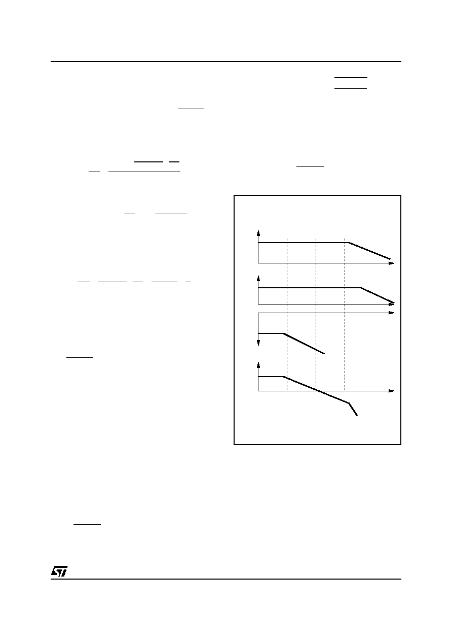
As can be easily see the bandwith is narrow and
the gain is low. It is possible to increase both
choosing an appropriate compensation of the Er-
ror amplifier.
The total bandwith should be, of course, at least a
decade lower of the 130KHz to avoid instability
problem. The bandwith guaranteed by the Error
amplifier has a Gmax of 80dB and a gain of 0dB
at 1MHz approximately, the real is some dB more
with a larger bandwith.
ACPW
30dB
130KHz
ACSENSE
20dB
210KHz
-31dB
LOAD
AX
19dB
1K
10K
100K
D95IN270A
L6246
9/12
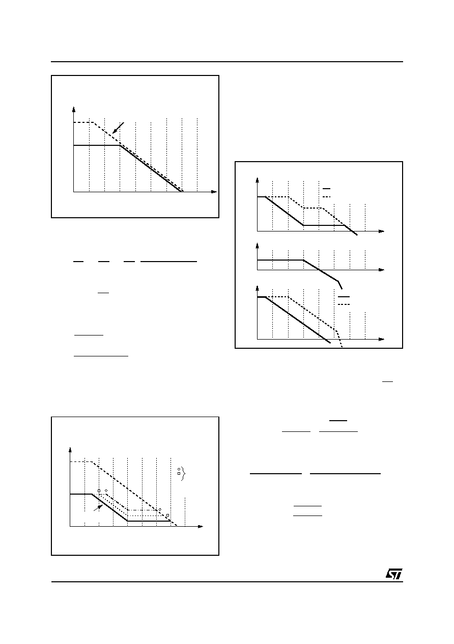
Using the compensation network of the draw of
pag.8, we have a error amplifier transfer function
of:
V
O
V
I
=
-
ZC
R1
=
-
R2
R1
1
+
scR3
1
+
sc
(
R3
+
R2
)
so:
Gmax (DC) =
R2
R1
= 1000 = 60dB
with R1 = 1M
and R2 = 1K
zero =
1
2
R3C
pole =
1
2
(
R3
+
R2
)
C
Note: Fpole is lower than Fzero
The best choice is to cancel the pole of the load
(at around 1KHz) with the zero of the compensa-
tion.
As can be seen the choice of the pole influence
overall in fixing the gain at high frequency.
The gain at high frequency must be choosen in
order to not create instability problem, because
more higher is this gain and lower is the second
pole that we have at high frequency.
If this pole is taken close to the other that we
have already seen at 130KHz and 210KHz, insta-
bility problems can arise.
Adding together AX |
dB
and A
CERR
|
dB
we ob-
taine the Aloop:
So the choice of the compensation network must
be done in order to fix at the beginning the Gmax
of the error amplifier depending on the ratio
R2
R1
.
To calculate the R3 and C values satisfying the
following system:
1
2
R3C
=
1
2
L
R
L
+
R
sense
Error amplifier zero equal to load pole
1
2
(
R3
+
R2
)
C
=
Admissible Bandwith
Gloop
=
=
130KHz
10
8912
=
1.5Hz
This example is for crossing the 0dB one decade
before the first pole of the Power Amplifier
(130KHz), starting with a Gloop max of 79dB.
ERROR AMPL. GAIN
(dB)
40
60
20
1K
10K
100K
D95IN271
100
120
80
1
10
100
1M
10M
OPEN LOOP GAIN
ACERR (dB)
40
60
20
1K
10K
100K
D95IN272
100
120
80
1
10
100
1M
10M
CLOSED LOOP
ACERR
X
X
DIFFERENTS
POLES
EXAMPLES
X
ACERR
(dB)
20
COMPENSATION AT 3Hz
AX(dB)
19
D95IN273
40
60
A
LOOP
(dB)
20
40
60
79
10
100
1K
10K
100K
1M
10M
COMPENSATION AT 100Hz
IS STABLE
IS NOT STABLE
L6246
10/12
PQFP44 (10 x 10)
A
A2
A1
B
Seating Plane
C
11
12
22
23
33
34
44
E3
D3
E1
E
D1
D
e
1
K
B
PQFP44
L
L1
0.10mm
.004
DIM.
mm
inch
MIN.
TYP.
MAX.
MIN.
TYP.
MAX.
A
2.45
0.096
A1
0.25
0.010
A2
1.95
2.00
2.10
0.077
0.079
0.083
B
0.30
0.45
0.012
0.018
c
0.13
0.23
0.005
0.009
D
12.95
13.20
13.45
0.51
0.52
0.53
D1
9.90
10.00
10.10
0.390
0.394
0.398
D3
8.00
0.315
e
0.80
0.031
E
12.95
13.20
13.45
0.510
0.520
0.530
E1
9.90
10.00
10.10
0.390
0.394
0.398
E3
8.00
0.315
L
0.65
0.80
0.95
0.026
0.031
0.037
L1
1.60
0.063
K
0
∞
(min.), 7
∞
(max.)
OUTLINE AND
MECHANICAL DATA
L6246
11/12

Information furnished is believed to be accurate and reliable. However, STMicroelectronics assumes no responsibility for the consequences
of use of such information nor for any infringement of patents or other rights of third parties which may result from its use. No license is
granted by implication or otherwise under any patent or patent rights of STMicroelectronics. Specification mentioned in this publication are
subject to change without notice. This publication supersedes and replaces all information previously supplied. STMicroelectronics products
are not authorized for use as critical components in life support devices or systems without express written approval of STMicroelectronics.
The ST logo is a registered trademark of STMicroelectronics
© 2003 STMicroelectronics ≠ Printed in Italy ≠ All Rights Reserved
STMicroelectronics GROUP OF COMPANIES
Australia - Brazil - Canada - China - Finland - France - Germany - Hong Kong - India - Israel - Italy - Japan - Malaysia - Malta - Morocco -
Singapore - Spain - Sweden - Switzerland - United Kingdom - United States.
http://www.st.com
L6246
12/12