GENERAL
12V (+/- 10%) OPERATION.
REGISTER BASED ARCHITECTURE
MINIMUM EXTERNAL COMPONENTS
BICMOS + VERTICAL DMOS (1.5mm)
VCM DRIVER
1.5A DRIVE CAPABILITY
0.9W TOTAL BRIDGE IMPEDANCE AT 25
∞
C
LINEAR MODE
PHASE SHIFT MODULATION (PWM MODE)
INSTANTANEOUS, (GLICH FREE) SWITCH
BETWEEN THE 2 MODES
CLASS AB OUTPUT DRIVERS
ZERO CROSSOVER DISTORSION
14 BIT DAC DEFINE OUTPUT CURRENT
SELECTABLE TRANSCONDUCTANCE
4 PROGRAMMABLE PARKING VOLTAGE
DYNAMIC BRAKE
SPINDLE DRIVER
2.0A DRIVE CAPABILITY
0.8W TOTAL BRIDGE IMPEDANCE AT 25
∞
C
BEMF, INTERNAL OR EXTERNAL, PROC-
ESSING
SENSOR-LESS MOTOR COMMUTATION
PROGRAMMABLE COMMUTATION PHASE
DELAY
LINEAR MODE AND CONSTANT TOFF PWM
OPERATION MODE
INTERNAL FREQUENCY LOCKED LOOP
SPEED CONTROL (FLL)
BEMF RECTIFICATION DURING RETRACT
BUILT-IN ALIGNAMENT&GO START-UP
INDUCTIVE SENSING START UP OPTION
RESYNCHRONIZATION
DYNAMIC & REVERSE BRAKE
CONTROLLABLE OUTPUT SLEW RATE
OTHER FUNCTIONS
12V AND 5V MONITORING WITH EXTERNAL
SET TRIP POINTS AND HYSTERESIS
POWER UP/DOWN SEQUENCING
LOW VOLTAGE SENSE
3.3V INPUT LOGIC COMPATIBILITY
THERMAL SHUTDOWN AND PRETHERMAL
WARNING
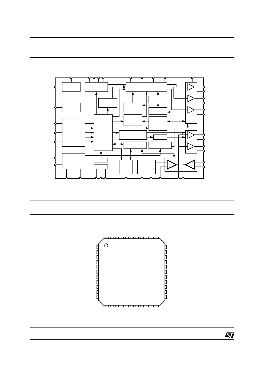
DESCRIPTION
The L6269 integrates into a single chip both spin-
dle and VCM controllers as well as power stages.
The device is designed for 12V disk drive applica-
tion requiring up to 2.0A of spindle and 1.5A of
VCM peak currents.
A serial port with up to 25 MHz capability provides
easy interface to the microprocessor. A register
controlled Frequency Locked Loop (FLL) allows
flexibility in setting the spindle speed. Integrated
BEMF processing, digital masking, digital delay,
and sequencing minimize the number of external
components required.
Power On Reset (POR) circuitry is included. Upon
detection of a low voltage condition, POR is as-
serted, the internal registers are reset, and spin-
dle power circuitry is tri-stated. The BEMF is recti-
fied providing power for actuator retraction
followed by dynamic spindle braking.
The device is built in BICMOS technology allow-
ing dense digital/analog circuitry to be combined
with a high power DMOS output stage.
This is preliminary information on a new product now in development. Details are subject to change without notice.
April 1999
Æ
TQFP44 (10x10mm)
ORDERING NUMBER: L6269
L6269
12V DISK DRIVE SPINDLE & VCM, POWER
& CONTROL "COMBO"
PRODUCT PREVIEW
BICMOS TECHNOLOGY
1/17

PIN DESCRIPTION (Pin Types: D = Digital, P = Power, A = Analog)
N.
Name
Function
1
FCOM
Output of the Spindle zero cross or Current Sense circuit.
2
CTAP
Spindle Central Tap used for differential BEMF sensing.
3
PWM/SLEW
RC network sets the Spindle Linear Slew Rate and PWM OFF-Tim e.
4
OUT_C
Spindle DMOS Half Bridge Output and Input C for BEMF sensing.
5
I_SENSE
Input to sense the voltage the SPINDLE Sense Resistor.
6
R_SENSE
Output connection for the Motor Current Sense Resistor to ground.
7
OUT_B
Spindle DMOS Half Bridge Output and Input B for BEMF sensing.
8
GND
Spindle Ground (Substrate).
9
R_SENSE
Output connection for the Motor Current Sense Resistor to ground.
10
OUT_A
Spindle DMOS Half Bridge Output and Input A for BEMF sensing.
11
INDEX
Input to allow Spindle to be locked to Index (servo) pulse.
12
BRK_CAP
Storage Capacitor for brake circuit. typically 5.9V.
13
VCC
+12V Power Supply for Spindle Power section.
14
DGND
Digital Ground.
15
SYS_CLK
Clock Frequency for system timers and counters.
16
SDEN
Serial Data Enable. Active high input pin for the serial port enable.
17
SDATA
Serial Port Data. Input/Output pin for serial data, 8bits of instruction/address followed by 8
bits of data. Open pin is at logic low as an input.
18
SCLK
Serial Port Data Clock. Positive edge triggered clock input for the serial data.
19
VDD
Digital/Analog power supply. +5V nominally.
20
V12/2
Reference Output for VCM control loop. Typically, half of the VCC except when parking.
21
FLL_FILTER
Speed loop R/C compensation connection used for FLL mode operation.
22
VCM_CAL
VCM loop offset voltage used for calibration.
23
CP
External Main Charge Pump Capacitor, Typically, Vz+Vcc is about 17.8V
24
CS
External Charge Pump Capacitor.
25
VCC
+12V Power Supply for VCM Power section.
26
VCM_A-
VCM Power Amplifier negative output terminal.
27
SENSE_IN+
Non inverting Input of the Sense Amplifier for VCM block.
28
VCM_GND
Ground for VCM Power section.
29
SENSE_IN-
Inverting Input of the Sense Amplifier for VCM block.
30
VCM_A+
VCM Power Amplifier positive output terminal.
31
VCC
+12V Power Supply for VCM Power section.
32
FLL_RES
Resistor for setting accurate bias current sources for the chip (62K required).
33
SW1
External ISOFET driver.
34
PORB
Power on Reset Output. Low signal indicates the failure of the supplies.
35
TR_5V
Set Point Input for 5V Supply Monitor ( 2V threshold, 100mV Hysteresis)
36
POR_DELAY
Capacitor connection to set the Power on Reset Delay (3V threshold, 2
µ
A charging)
37
SENSE_OUT
Output of the Sense Amplifier.
38
ERROR_OUT
Output of the Error Amplifier.
39
ERROR_IN
Inverting Input of the Error Amplifier.
40
TR_12V
Set Point Input for 12V Supply Monitor (2V threshold, 100mV Hysteresis)
41
DAC
Output of the VCM DAC.
42
AGND
Analog Ground. For bang gap voltage reference.
43
VCC
+12V Power Supply for Spindle Power section.
44
SPN_COMP
External RC network that defines the compensation of the Spindle Transconductance Loop
in Linear Mode.
L6269
3/17
ELECTRICAL CHARACTERISTICS (All specifications are for 0 < T
amb
< 70
∞
C, V
CC
= 12V; V
DD
= 5V,
FLL_RES = 62k
, unless otherwise specified.)
Symbol
Parameter
Test Condition
Min.
Typ.
Max.
Unit
POWER SUPPLIES
V
CC
12V Supply
10.8
13.2
V
I
VCC
V
CC
Current
SPINDLE + VCM
20
mA
SPINDLE ONLY
7
mA
VCM ONLY
12
mA
V
rectified
V
CC
Supply Rectified
3.5
13.2
V
V
dd
5V supply
4.5
5.5
V
I
Vdd
5V supply
SPINDLE + VCM
6
mA
SPINDLE ONLY
7
mA
VCM ONLY
12
mA
ABSOLUTE MAXIMUM RATINGS
Symbol
Parameter
Value
Unit
V
CC
Maximum Supply voltage
-0.5 to 14
V
V
dd
Maximum Logic supply
-0.5 to 6
V
V
in max
Maximum digital input voltage
V
dd
+0.3V
V
V
in min
Minimum digital input voltage
GND - 0.3V
V
SPINDLE I
peak
Spindle peak sink/source output current
2.1
A
VCM I
peak
VCM peak sink/source output current
1.6
A
P
tot
(*)
Maximum Total Power Dissipation
2.0
W
T
stg
, T
j
Maximum Storage/Junction Temperature
-40 to 150
∞
C
THERMAL DATA
Symbol
Parameter
Value
Unit
R
th j-case
Thermal Resistance Junction to Case
11
∞
C/W
R
th j-amb
(*)
Thermal Resistance to Junction to ambient
40
∞
C/W
(*) In typical application with multilayer 120X120mm Printed Circuit Board
RECOMMENDED OPERATING CONDITIONS
Symbol
Parameter
Value
Unit
V
CC
Supply voltage
10.8 to 13.2
V
V
dd
Maximum Logic supply
4.5 to 5.5
V
T
amb
Operating Ambient Temperature
0 to 70
∞
C
T
j
Junction Temperature
0 to 125
∞
C
L6269
4/17