 | –≠–ª–µ–∫—Ç—Ä–æ–Ω–Ω—ã–π –∫–æ–º–ø–æ–Ω–µ–Ω—Ç: L6375D | –°–∫–∞—á–∞—Ç—å:  PDF PDF  ZIP ZIP |
1/12
L6375
February 2000
This is preliminary information on a new product now in development or undergoing evaluation. Details are subject to change with out notice.
s
0.5A OUTPUT CURRENT
s
8V TO 35V SUPPLY VOLTAGE RANGE
s
NON DISSIPATIVE SHORT CIRCUIT
PROTECTION
s
THERMAL SHUTDOWN
s
OPEN GROUND PROTECTION
s
NEGATIVE VOLTAGE CLAMPING FOR FAST
DEMAGNETIZATION
s
UNDERVOLTAGE LOCKOUT WITH
HYSTERESIS
s
OPEN LOAD DETECTION
s
TWO DIAGNOSTIC OUTPUTS
s
OUTPUT STATUS LED DRIVER
s
IMMUNITY AGAINST BURST TRANSIENT
(IEC 801-4), see application schematic.
s
ESD PROTECTION (HUMAN BODY MODEL
±
2KV)
DESCRIPTION
The L6375 is a monolithic fully protected, full diag-
nostic 0.5A Intelligent Power Switch. it is designed to
drive any kind of R-L-C load with controlled output
voltage slew rate and non dissipative short circuit
protection. An internal Clamping Diode enables the
fast demagnetization of inductive loads. Diagnostic
for CPU feedback and extensive use of electrical pro-
tections make this device extremely rugged and spe-
cially suitable for industrial automation applications.
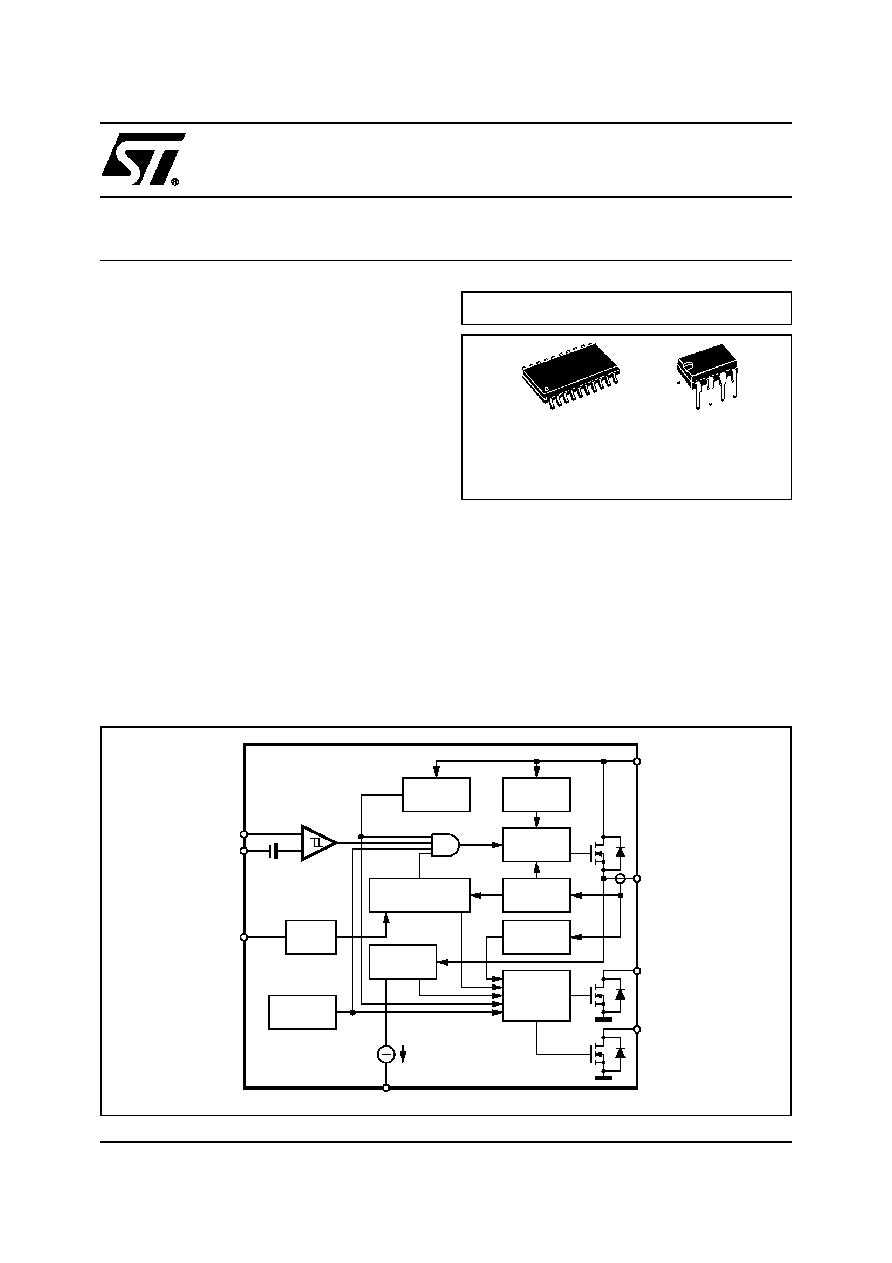
SO20
MINIDIP
ORDERING NUMBERS:
L6375D
L6375
PRELIMINARY DATA
0.5A INDUSTRIAL INTELLIGENT POWER SWITCH
BLOCK DIAGRAM
UNDER
VOLTAGE
CHARGE
PUMP
DRIVER
NON DISSIPATIVE
SHORT CIRCUIT
CURRENT
LIMITATION
OPEN LOAD
DETECTION
OUTSTATUS
DIAGNOSTIC
THERMAL
PROTECTION
OSC
+
-
1.4V
INPUT
IN+
IN-
Con
OUTPUT STATUS
3mA
DIAG2
DIAG1
OUT
V
S
D95IN208B
MULTIPOWER BCD TECHNOLOGY
L6375
2/12
PIN FUNCTION (Pin numbering referred to Minidip package)
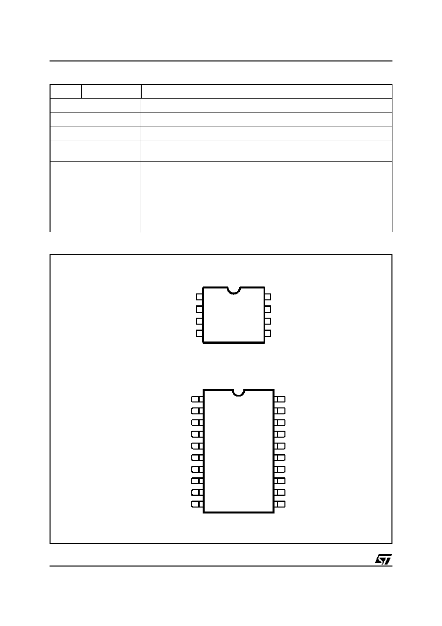
PIN CONNECTION (Top view)
N
∞
Pin
Description
1
GND
Ground
2
OUT
High side output. Controlled output with current limitation
3
Vs
Supply voltage input. Range with under voltage monitoring
4
OUTPUT STATUS
Led driver to signal the status of the output pin. The pin is active ( sources current )
when the output is considered high. (See fig. 1)
5
DIAG1
Diagnostic 1 output. This open drain reports the IC working conditions. (See
Diagnostic truth table)
6
DIAG2
Diagnostic 2 output. This open drain reports the IC working conditions. (See
Diagnostic truth table)
7
IN+
Comparator non inverting input
8
ON DELAY
Delay setting for overcurrent diagnostic
N.C.
GND
N.C.
OUTPUT
N.C.
N.C.
V
S
N.C.
N.C.
N.C.
N.C.
DIAG2
N.C.
DIAG1
INPUT+
N.C.
ON DELAY
N.C.
1
3
2
4
5
6
7
8
9
18
17
16
15
14
12
13
11
19
10
20
OUTPUT STATUS
N.C.
GND
OUTPUT
V
S
OUTPUT STATUS
1
3
2
4
DIAG2
DIAG1
INPUT +
ON DELAY
8
7
6
5
MINIDIP
SO20

3/12
L6375
ABSOLUTE MAXIMUM RATINGS (Pin numbering referred to Minidip package)
THERMAL DATA
Symbol
Pin
Parameter
Value
Unit
V
s
3
Supply Voltage (tw < 10 ms)
50
V
V
s
3
Supply Voltage (DC)
40
V
V
s
-V
out
3 vs 2
Supply to Output Differential voltage
internally limited
V
od
5
Externally Forced Voltage
-0.3 to 7
V
I
od
5
Externally Forced Current
±
1
mA
I
out
2
Output Current (see also Isc)
internally limited
V
out
2
Output Voltage
internally limited
V
P
tot
Power Dissipation
internally limited
V
diag
5.6
External voltage
-0.3 to 40
V
I
diag
5.6
Externally forced current
-10 to 10
mA
I
i
7
Input Current
20
mA
V
i
7
Input Voltage
-10 to Vs +0.3
V
T
op
Ambient temperature, operating range
-25 to 85
∞
C
T
j
Junction temperature, operating range
(see Overtemperature Protection)
-25 to 125
∞
C
T
stg
Storage temperature
-55 to 150
∞
C
E
I
Energy Induct. Load T
J
= 85
∞
C
200
mJ
Symbol
Parameter
Minidip
SO20
Unit
R
th j-case
Thermal Resistance Junction to Case
Max.
∞
C/W
R
th j-amb
Thermal Resistance Junction to Ambient
Max.
100
90
∞
C/W
L6375
4/12
ELECTRICAL CHARACTERISTCS
(V
S
= 24V; T
j
= ≠25 to +125
∞
C, unless otherwise specified; pin numbering referred to Minidip package)
Symbol
Pin
Parameter
Test Condition
Min.
Typ.
Max.
Unit
V
smin
3
Supply Voltage for Valid
Diagnostic
I
diag
= >0.5mA;V
diag
= 1.5V;
4
35
V
V
s
3
Operative Supply Voltage
8
24
35
V
V
sth1
3
Undervoltage Threshold 1
(See fig. 2)
7
7.5
8
V
V
sth2
3
Undervoltage Threshold 2
(See fig. 2)
6.5
7
7.5
V
V
shys
3
Under Voltage Hysteresis
300
500
700
mV
I
q
3
Quiescent Current
Output Open
800
µ
A
I
qo
3
Quiescent Current
Output On
1.6
mA
V
ith
7
Input Threshold Voltage
0.8
1.3
2
V
V
iths
7
Input Threshold Hysteresis
50
400
mV
V
il
7
Input Low Level Voltage
-7
0.8
V
V
ih
7
Input High Level Voltage
V
s
< 18V
2
V
s
-3
V
V
ih
7
Input High Level Voltage
V
s
> 18V
2
15
V
I
ib
7
Input Bias Current
V
i
= -7 to 15V
-250
250
µ
A
I
dch
5
Delay Capacitor Charging
Current
ON DELAY pin shorted to
Ground
2.5
µ
A
V
don
Output Voltage Drop
I
out
= 500mA T
j
= 25
∞
C
T
j
= 125
∞
C
I
out
=
625mA T
j
= 25
∞
C
T
j
= 125
∞
C
200
320
250
400
280
440
350
550
mV
mV
mV
mV
I
olk
2
Output Leakage Current
V
i
= LOW; V
out
=0
100
µ
A
V
ol
2
Output Low State Voltage
V
i
= HIGH; pin floating
0.8
1.5
V
V
cl
2
Internal Voltage Clamp (V
s
-V
out
)
I
o
= 200mA
single pulsed =300
µ
s
48
53
58
V
I
sc
2
Short Circuit Output Current
V
s
= 8 to 35V; R
l
= 2
;
0.75
1.1
1.5
A
I
old
2
Open Load Detection Current
V
i
= V
ih
; T
amb
= 0 to +85
∞
C
1
3
6
mA
V
oth1
5.6
Output Status Threshold 1
Voltage
(See fig. 1)
4.5
5
5.5
V
V
oth2
5.6
Output Status Threshold 2
Voltage
(See fig. 1)
4
4.5
5
V
V
ohys
5.6
Output Status Threshold
Hysteresis
(See fig. 1)
300
500
700
mV
I
osd
5.6
Output Status Source Current
V
out
> V
oth1
; V
os
= 2.5V
2
4
mA

5/12
L6375
V
osd
5.6
Active Output Status Driver
Drop Voltage
V
s
≠ V
o
s
; I
os
= 2mA
T
amb
=
0 to +85
∞
C
1.5
3
V
I
oslk
5.6
Output Status Driver Leakage
Current
V
out
< V
oth2
; V
os
=
0V
V
S
= 18 to 35V
25
µ
A
V
dgl
5.6
Diagnostic Drop Voltage
D1 / D2 = L ; I
diag
= 0.5mA
D1 / D2 = L ; I
diag
= 3mA
40
250
mV
mV
I
dglk
5.6
Diagnostic Leakage Current
D1 / D2 = H ; 0 < V
dg
< V
s
V
S
= 15.6 to 35V
5
µ
A
T
max
Over Temperature Upper
Threshold
150
∞
C
T
hys
Over Temperature Hysteresis
20
∞
C
AC OPERATION (
pin numbering referred to Minidip package)
t
r
-t
f
2
Rise or Fall Time
Vs = 24V; R
l
=70
R
l
to ground
20
µ
s
t
d
2
Delay Time
Vs = 24V; Rl =70
R
l
to ground
5
µ
s
dV/dt
2
Slew Rate (Rise and Fall Edge)
50pF < C
DON
< 2nF
7
1
15
V/
µ
s
t
ON
8
On time during Short Circuit
Condition
128
µ
s/pF
t
OFF
8
Off time during Short Circuit
Condition
64
µ
s/pF
f
max
Maximum Operating Frequency
25
KHz
SOURCE DRAIN NDMOS DIODE
V
f
Forward On Voltage
@ Ifsd = 625mA
1
1.5
V
I
fD
Forward Peak Voltage
t = 10ms; d = 20%
2
A
t
rr
Reverse Recovery Time
I
f
= 625mA di/dt = 25A/
µ
s
200
ns
t
fr
Forward Recovery Time
50
ns
Symbol
Pin
Parameter
Test Condition
Min.
Typ.
Max.
Unit
ELECTRICAL CHARACTERISTCS (Continued)

L6375
6/12
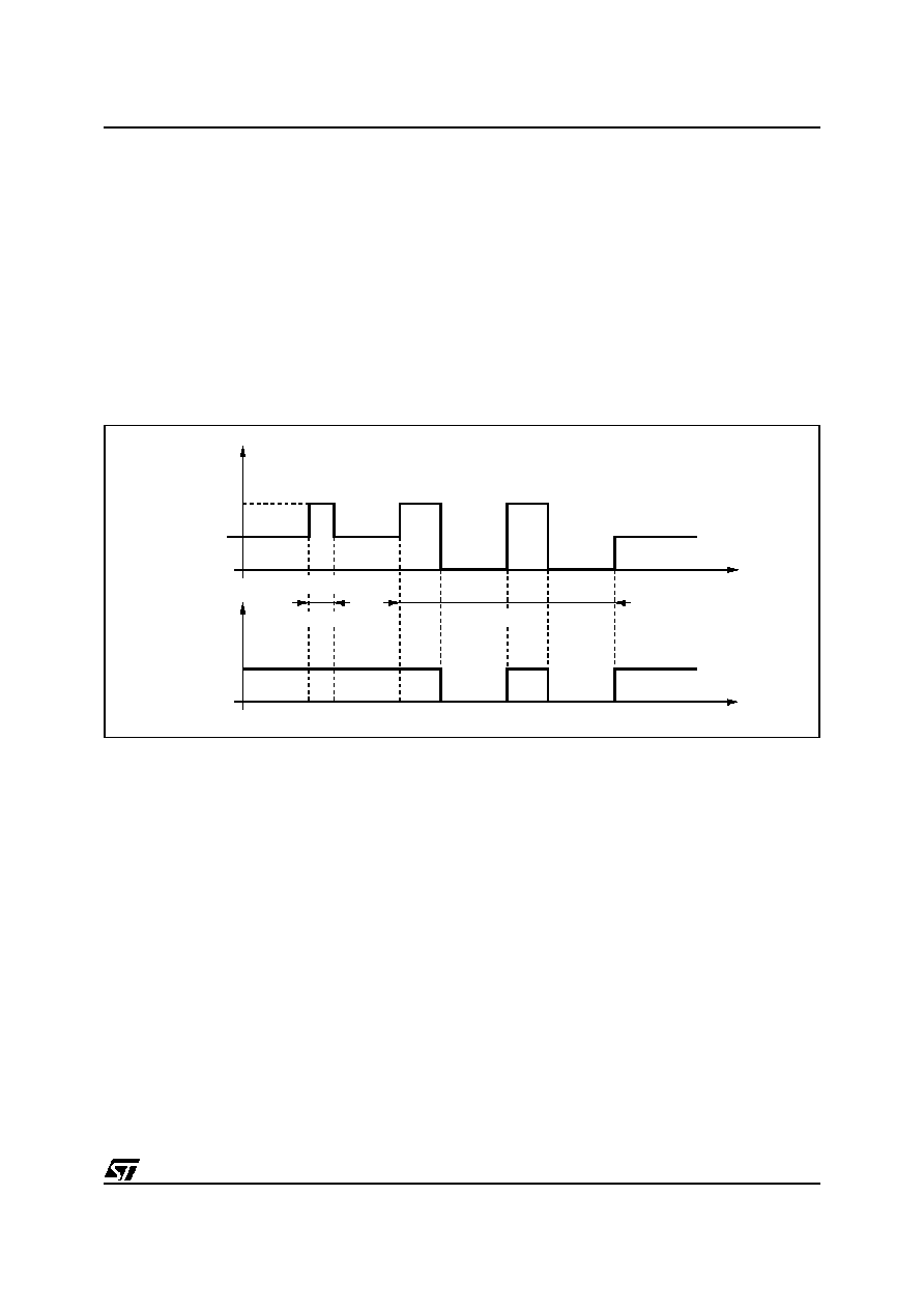
Figure 1. Switching Waveforms
INPUT SECTION
An Single ended Input TTL/CMOS compatible with wide voltage range and high noise immunity (thanks to a
built in hysteresis) is available.
OVER TEMPERATURE PROTECTION (OVT)
An on-chip Over Temperature Protection provides an excellent protection of the device in extreme conditions.
Whenever the temperature - measured on a central portion of the chip- exceeds Tmax=150 C (typical value)
the device is shut off, and the DIAG2 output goes LOW. Normal operation is resumed as the chip temperature
(normally after few seconds) falls below Tmax-Thys= 130 C (typical value). The hysteresis avoid thats an inter-
mittent behaviour take place.
UNDER VOLTAGE PROTECTION (UV)
The supply voltage is expected to range from 8 to 35 V. In this range the device operates correctly. To avoid
any misfunctioning the supply voltage is continuously monitored to provide an under voltage protection. As Vs
falls below Vsth-Vshys (typically 7.5 V, see fig.1) the output power MOS is switched off and DIAG1 and DIAG2
(see Diagnostic truth table). Normal operation is resumed as soon as Vs exceeds Vsth. The hysteretic behaviour
prevents intermittent operation at low supply voltage.
OVER CURRENT OPERATION
In order to implement a short circuit protection the output power MOS is driven in linear mode to limit the output
current to the Isc (1.1A typical value). This condition (current limited to the Isc value) lasts for a Ton time interval,
that can be set by means of a capacitor (Cdon) connected to the ON DELAY pin according to the following for-
mula:
Ton = 1.28 msec/pF
for
50pF<Cdon< 2nF
After the Ton interval has expired the output power MOS is switched off for the Toff time interval with:
Toff = 64 ∑Ton.
When also the Toff interval has expired, the out-put power MOS is switched ON. At this point in time two con-
50%
50%
td
td
t
90%
90%
10%
10%
tf
tr
t
Vin
Vout
D94IN127A
50%
50%
7/12
L6375
ditions may occur
A) the overload is still present, and then the output power MOS is again driven in linear mode (limiting
the output current to Isc) for another Ton, starting a new cycle, or
B) the overload condition is removed, and the output power MOS is no longer driven in linear mode.
All these occurrences are presented on the DIAG2 pin (see fig 2).
We call this unique feature
Non Dissipative Short Circuit Protection and it ensures a very safe operation even
in permanent overload conditions. Note that choosing the most appropriate value for the Ton interval (i.e. the
value of the Cdon capacitor) a delay (the Ton itself) will prevent that a misleading Short Circuit information is
presented on the DIAG2 output, when driving capacitive loads (that acts like short circuit in the very beginning)
or Incandescent Lamp (a cold filament has a very low resistive value). The Non Dissipative Short Circuit Pro-
tection can be disabled (keeping Ton = 0 but with the output current still limited to Isc, and Diagnostic dis-
abled)simply shorting to ground the the ON DELAY pin.
Figure 2. Non Dissipative Short Circuit Protection Operation
DIAGNOSTIC LOGIC
The operating conditions of the device are permanently monitored and the following occurrences are signalled
via the DIAG1/DIAG2 open-drain output pins see: diagnostic Truth Table.
- Short Circuit versus ground.
- Short Circuit versus V
S
.
- Under Voltage(UV)
- Over Temperature (OVT)
- Open Load, if the output current is less than 3mA (typical value).
DEMAGNETIZATION OF INDUCTIVE LOADS
An internal zener diode, limiting the voltage across the Power MOS to between 50 and 60V (V
cl
), provides safe
and fast demagnetization of inductive loads without external clamping devices. The maximum energy that can
be absorbed from an inductive load is specified as 200mJ (at T
j
= 85
∞
C)
OUTPUT
CURRENT
t
ON
t
ON
t
OFF
t
OFF
Time
t<t
ON
DIAG
(active low)
Time
Short Circuit
Short Circuit
Isc
Iout
D94IN105

L6375
8/12
DIAGNOSTIC TRUTH TABLE
Figure 3. Inductive Load Equivalent Circuit
Figure 4. External Demagnetisation Circuit (versus ground)
Diagnostic Conditions
Input
Output
DIAG1
DIAG2
Normal Operation
L
H
L
H
H
H
H
H
Open Load Condition (I
o
< I
old
)
L
H
L
H
H
L
H
H
Short to V
S
L
H
H
H
L
L
H
H
Short Circuit to Ground (I
O
= I
SC
)
(pin ON-DELAY grounded)
H
H
L
H
H
H
H
Output DMOS Open
L
H
L
L
H
L
H
H
Overtemperature
L
H
L
L
H
H
L
L
Sumplay Undervoltage (V
S
< V
sth2
)
L
H
L
L
L
L
L
L
50V
L
+V
S
I
S
V
S
RL
I
O
OUTPUT
D95IN215
DRIVER
VS
OVC
OUT
RS
SHORT CIRCUIT
CONTROL
UV
CURRENT
LIMIT
D94IN112
V
Z
V
Z
< V
cl (min)
- V
S (max)

9/12
L6375
Figure 5. External Demagnetisation Circuit (versus V
S
)
Figure 6. Application Schematic
DRIVER
VS
OVC
OUT
RS
SHORT CIRCUIT
CONTROL
UV
CURRENT
LIMIT
D94IN111A
V
Z
V
S (max)
< V
Z
< V
cl (min)
V
S
UNDER
VOLTAGE
CHARGE
PUMP
DRIVER
NON DISSIPATIVE
SHORT CIRCUIT
CURRENT
LIMITATION
OPEN LOAD
DETECTION
OUTSTATUS
DIAGNOSTIC
THERMAL
PROTECTION
OSC
+
-
1.4V
INPUT
IN+
Con
OUTPUT STATUS
3mA
DIAG2
DIAG1
OUT
V
S
Transil, ST1,5KExx (IEC801-5)
2.2
µ
F, electrolytic
10nF, ceramic
(IEC801-4, IEC801-4)
L6375
10/12
1
1
0
11
20
A
e
B
D
E
L
K
H
A1
C
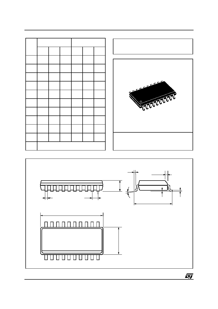
SO20MEC
h x 45
∞
SO20
DIM.
mm
inch
MIN.
TYP.
MAX.
MIN.
TYP.
MAX.
A
2.35
2.65
0.093
0.104
A1
0.1
0.3
0.004
0.012
B
0.33
0.51
0.013
0.020
C
0.23
0.32
0.009
0.013
D
12.6
13
0.496
0.512
E
7.4
7.6
0.291
0.299
e
1.27
0.050
H
10
10.65
0.394
0.419
h
0.25
0.75
0.010
0.030
L
0.4
1.27
0.016
0.050
K
0
∞
(min.)8
∞
(max.)
OUTLINE AND
MECHANICAL DATA

11/12
L6375
Minidip
DIM.
mm
inch
MIN.
TYP.
MAX.
MIN.
TYP.
MAX.
A
3.32
0.131
a1
0.51
0.020
B
1.15
1.65
0.045
0.065
b
0.356
0.55
0.014
0.022
b1
0.204
0.304
0.008
0.012
D
10.92
0.430
E
7.95
9.75
0.313
0.384
e
2.54
0.100
e3
7.62
0.300
e4
7.62
0.300
F
6.6
0.260
I
5.08
0.200
L
3.18
3.81
0.125
0.150
Z
1.52
0.060
OUTLINE AND
MECHANICAL DATA

Information furnished is believed to be accurate and reliable. However, STMicroelectronics assumes no responsibility for the consequences
of use of such information nor for any infringement of patents or other rights of third parties which may result from its use. N o license is granted
by implication or otherwise under any patent or patent rights of STMicroelectronics. Specifications mentioned in this publication are subject
to change without notice. This publication supersedes and replaces all information previously supplied. STMicroelectronics products are not
authorized for use as critical components in life support devices or systems without express written approval of STMicroelectronics.
The ST logo is a registered trademark of STMicroelectronics
Æ
1999 STMicroelectronics - All Rights Reserved
STMicroelectronics GROUP OF COMPANIES
Australia - Brazil - China - Finland - France - Germany - Hong Kong - India - Italy - Japan - Malaysia - Malta - Morocco - Singapore - Spain
- Sweden - Switzerland - United Kingdom - U.S.A.
http:/ /www.st.com
12/12
L6375