 | –≠–ª–µ–∫—Ç—Ä–æ–Ω–Ω—ã–π –∫–æ–º–ø–æ–Ω–µ–Ω—Ç: L6376D | –°–∫–∞—á–∞—Ç—å:  PDF PDF  ZIP ZIP |
L6376
0.5A HIGH-SIDE DRIVER
QUAD INTELLIGENT POWER SWITCH
0.5 A FOUR INDEPENDENT OUTPUTS
9.5 TO 35 V SUPPLY VOLTAGE RANGE
INTERNAL CURRENT LIMIT
NON-DISSIPATIVE OVER-CURRENT PRO-
TECTION
THERMAL SHUTDOWN
UNDER VOLTAGE LOCKOUT WITH HYS-
TERESYS
DIAGNOSTIC OUTPUT FOR UNDER VOLT-
AGE, OVER TEMPERATURE AND OVER
CURRENT
EXTERNAL ASYNCHRONOUS RESET IN-
PUT
PRESETTABLE DELAY FOR OVERCUR-
RENT DIAGNOSTIC
OPEN GROUND PROTECTION
IMMUNITY AGAINST BURST TRANSIENT
(IEC 801-4)
ESD PROTECTION (HUMAN BODY MODEL
±
2KV)
DESCRIPTION
This device is a monolithic quad Intelligent Power
Switch in Multipower BCD Technology, for driving
inductive, capacitive or resistive loads. Diagnostic
for CPU feedback and extensive use of electrical
protections make this device inherently indis-
tructible and suitable for general purpose indus-
trial applications.
September 2003
Æ
POWERDIP
16+2+2
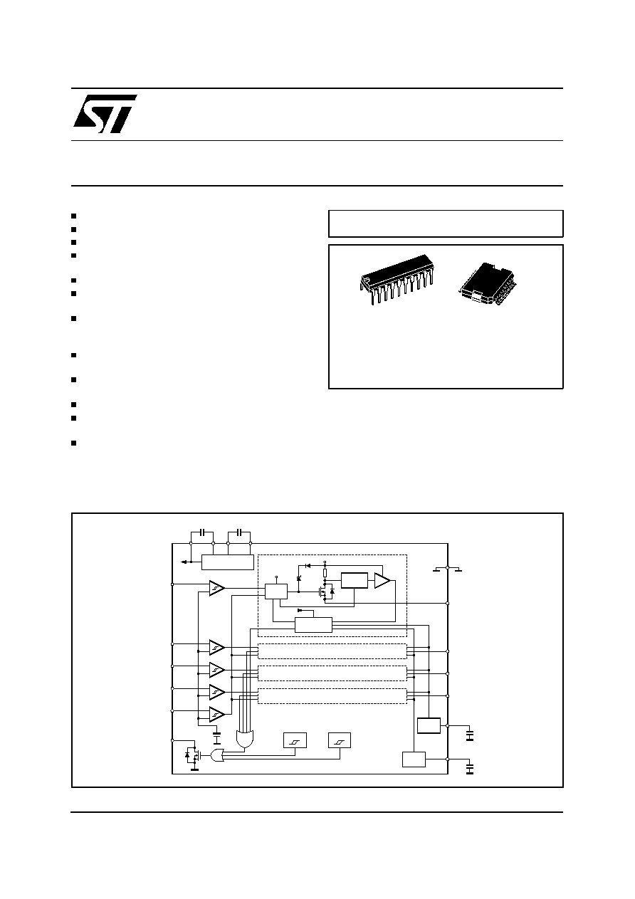
MULTIPOWER BCD TECHNOLOGY
CHARGE PUMP
DRIVER
VS
VCP
+
-
+
-
+
-
+
-
VS
OVC
I1
I2
I3
I4
R
DIAG
220nF
22nF
VCP
VS
VC
VP
OVT
UV
ON
OSC
OFF DELAY
ON DELAY
CDON
CDOFF
O4
O3
O2
O1
GND
D94IN076C
1.25V
RS
SHORT CIRCUIT
CONTROL
OFF
OSC
UV
CURRENT
LIMIT
+
-
BLOCK DIAGRAM
ORDERING NUMBERS: L6376 (DIP)
L6376D (PSO)
PowerSO20
1/12
ABSOLUTE MAXIMUM RATINGS (Pin numering referred to PowerSO20 package)
Symbol
Pin
Parameter
Value
Unit
V
s
6
Supply Voltage (t
w
< 10ms)
50
V
Supply Voltage (DC)
40
V
V
s
- V
out
Difference between supply voltage and output voltage
internally limited
V
id
16, 17
Externally Forced Voltage
-0.3 to 7
V
I
id
Externally Forced Current
±
1
mA
I
i
12, 13,
14, 15,
18
Channel Input Current (forced)
±
2
mA
V
i
Channel Input Voltage
-0.3 to 40
V
I
out
2, 3,
8, 9
Output Current (see also I
sc
)
internally limited
V
out
Output Voltage
internally limited
E
il
Energy Inductive Load (T
j
=125∞C); Each Channel
200
mJ
P
tot
Power Dissipation
internally limited
V
diag
19
External voltage
-0.3 to V
s
+0.7
V
I
diag
Externally forced current
-10 to 10
mA
T
op
Ambient temperature, operating range
-25 to 85
∞
C
T
j
Junction temperature, operating range (see
Overtemperature Protection)
-25 to 125
∞
C
T
stg
Storage temperature
-55 to 150
∞
C
PIN CONNECTIONS (Top view)
VS
VCP
O2
O1
GND
I1
GND
I2
I3
1
3
2
4
5
6
7
8
9
OFF DELAY
R
DIAG
GND
GND
O4
O3
VP
VC
20
19
18
17
16
14
15
13
12
D93IN030B
I4
10
ON DELAY
11
POWERDIP
GND
O1
I1
O3
VP
V
S
VC
VCP
O2
O4
GND
10
8
9
7
6
5
4
3
2
13
14
15
16
17
19
18
20
12
1
11
GND
D95IN217
I2
I3
ON DELAY
I4
OFF DELAY
R
DIAG
GND
PowerSO20
L6376
2/12
PIN DESCRIPTION (Pin numering referred to PowerSO20 package).
No
Pins
Function
6
V
S
Positive supply voltage.
An internal circuit, monitoring the supply voltage, maintains the IC in off-state until V
S
reaches 9V or when V
S
falls under 8.5V.
The diagnostic is availlable since V
S
= 5V.
7
V
CP
Switch driver supply.
To minimize the output drop voltage, a supply of about 10V higher than V
S
is required. In
order to use the built-in charge pump, connect a filter capacitor from pin1 to pin.
The suggested value assures a fast transition and a low supply ripple even in worse
condition. Using the four channels contemporarily, values less than 68nF have to be
avoided.
2, 3,
8, 9
O
1
, O
2
, O
3
, O
4
High side outputs.
Four independently controlled outputs with built-in current limitation.
1, 10,
11, 20
GND
Ground and power dissipating pins.
These pins are connected to the bulk ground of the IC, so are useful for heat dissipation.
12,13,
14, 15
I
1
, I
2
, I
3
, I
4
Control inputs.
Four independent control signals. The output is held off until the voltage at the
corresponding input pin reaches 1.35V and is turned off when the voltage at the pin goes
below 1.15V.
16
ON DELAY
Programmable ON duration in short circuit.
If an output is short circuited to ground or carryng a current exceeding the limit, the output
is turned-off and the diagnostic activation are delayed. This procedure allows the driving of
hard surge current loads.
The delay is programmed connecting a capacitor (50pF to 15nF) versus ground with the
internal time constant of 1.28
µ
s/pF. The function can be disabled short circuiting this pin to
ground.
17
OFF DELAY
Programmable OFF duration in short circuit.
After the short circuit or overcurrent detection, the switch is held off before the next
attempt to switch on again.
The delay is programmed connecting a capacitor (50pF to 15nF) versus ground with the
internal time constant of 1.28
µ
s/pF.
Short circuiting this pin to ground the OFF delay is 64 times the ON delay.
18
R
Asyncronous reset input.
This active low input (with hysteresis), switch off all the outputs independently from the
input signal. By default it is biased low.
19
DIAG
Diagnostic output.
This open drain output reports the IC working condition. The bad condition (as
undervoltage, overcurrent, overtemperature) turns the output low.
5
V
C
Pump oscillator voltage.
At this pin is available the built-in circuitry to supply the switch driver at about 10V higher
than V
S
. To use this feature, connect a capacitor across pin 4 and pin 5.
The suggested value assures a fast transition and a minimum output drop voltage even in
worse condition. Using the four channels contemporarily, values less than 6.8nF have to
be avoided.
4
V
P
Bootstrapped voltage.
At this pin is available the 11V oscillation for the charge pump, at a typical frequency of
200kHz.
L6376
3/12
ELECTRICAL CHARACTERISTICS (V
s
= 24V; T
j
= -25 to 125
∞
C; unless otherwise specified.)
DC OPERATION (Pin numering referred to PowerSO20 package).
Symbol
Pin
Parameter
Test Condition
Min.
Typ.
Max.
Unit
V
s
6
Supply Voltage
9.5
24
35
V
V
sth
UV UpperThreshold
8.5
9
9.5
V
V
shys
UV Hysteresis
200
500
800
mV
I
qsc
Quiescent Current
Outputs ON, No load
3
5
mA
V
il
12,13,
14,15,
18
Input Low Level
0
0.8
V
V
ih
Input High Level
2
40
V
I
bias
Input Bias Current
V
i
= 0V
-5
-1
0
µ
A
V
i
= 40V
0
5
20
µ
A
V
ihys
Input Comparators Hysteresis
100
200
400
mV
lim
OVT Upper Threshold
150
∞
C
H
Threshold Hysteresis
20
30
∞
C
I
sc
2, 3,
8, 9
Short Circuit Current
V
s
=9.5 to 35V; R
l
=2
0.65
0.9
1.2
A
Output Voltage Drop
I
out
=500mA
;
T
j
=25
∞
C
320
500
mV
I
out
=500mA
;
T
j
=125
∞
C
460
640
mV
I
olk
Output Leakage Current
V
o
=0V; V
i
<0.8V
100
µ
A
V
cl
Internal Voltage Clamp
(V
s
-V
o
each Output)
I
o
=100mA
single pulsed T
p
=300
µ
s
47
52
57
V
V
ol
Low State Output Voltage
V
i
= V
il
; R
L
=
0.8
1.5
V
I
dlkg
19
Diagnostic Output Leakage
Diagnostic Off
25
µ
A
V
diag
Diagnostic Output Voltage
Drop
I
diag
= 5mA
1.5
V
I
dch
16, 17
Delay Capacitors Charge
Current
40
µ
A
L6376
4/12
AC OPERATION (Pin numering referred to PowerSO20 package).
Symbol
Pin
Parameter
Test Condition
Min.
Typ.
Max.
Unit
t
r
-t
f
2, 3, 8, 9
Rise or Fall Time
V
s
= 24V; R
l
= 47
R
l
to ground
3.8
µ
s
t
d
12 vs 9
13 vs 8
14 vs 3
15 vs 2
Delay Time
1
µ
s
dV/dt
2, 3,
8, 9
Slew Rate (Rise and Fall
Edge)
V
s
= 24V; R
l
= 47
RISE
R
l
to ground FALL
3
4
5
7.6
7
10
V/
µ
s
t
ON
16
On Time during Short
Circuit Condition
50 pF < C
DON
< 15nF
1.28
µ
s/pF
t
OFF
17
Off Time during Short
Circuit Condition
pin 13 grounded
64
t
ON
50pF < C
DOFF
< 15nF
1.28
µ
s/pF
f
max
Maximum Operating
Frequency
25
kHz
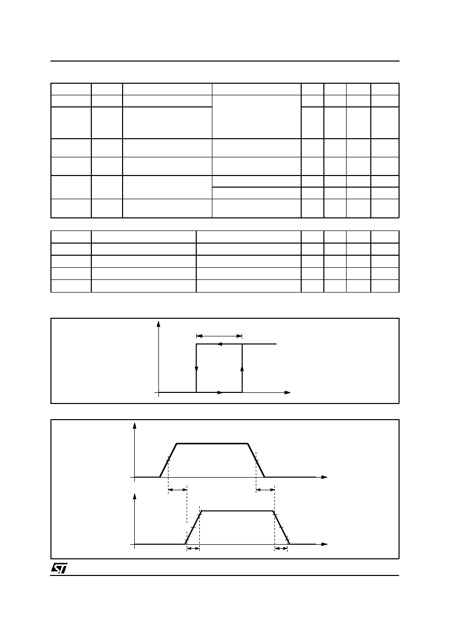
SOURCE DRAIN NDMOS DIODE
Symbol
Parameter
Test Condition
Min.
Typ.
Max.
Unit
V
fsd
Forward On Voltage
I
fsd
= 500mA
1
1.5
V
I
fp
Forward Peak Current
t
p
= 10ms; duty cycle = 20%
1.5
A
t
rr
Reverse Recovery Time
I
fsd
= 500mA; dI
fsd
/dt = 25A/
µ
s
200
ns
t
fr
Forward Recovery Time
50
ns
50%
50%
td
td
t
90%
90%
10%
10%
tf
tr
t
Vin
Vout
D94IN127A
50%
50%
SWITCHING WAVEFORMS
Vs
D94IN126A
Vsth
Vshys
UNDERVOLTAGE COMPARATOR HYSTERESIS
L6376
5/12
THERMAL CHARACTERISTICS
R
th j-pins
DIP16+2+2. The thermal resistance is re-
ferred to the thermal path from the dissipat-
ing region on the top surface of the silicon
chip, to the points along the four central pins
of the package, at a distance of 1.5 mm
away from the stand-offs.
R
th j-amb1
If a dissipating surface, thick at least 35
µ
m,
and with a surface similar or bigger than the
one shown, is created making use of the
printed circuit.
Such heatsinking surface is considered on
the bottom side of an horizontal PCB (worst
case).
R
th j-amb2
If the power dissipating pins (the four central
ones), as well as the others, have a mini-
mum thermal connection with the external
world (very thin strips only) so that the dissi-
pation takes place through still air and
through the PCB itself.
It is the same situation of point above, with-
out any heatsinking surface created on pur-
pose on the board.
Additional data on the PowerDip and the
PowerSO20 package can be found in:
Application Note AN467:
Thermal Characteristics of the PowerDip
20,24 Packages Soldered on 1,2,3 oz.
Copper PCB
Application Note AN668:
A New High Power IC Surface Mount Pack-
age: PowerSO20 Power IC Packaging from
Insertion to Surface Mounting.
THERMAL DATA
Symbol
Parameter
DIP16+2+2
PowerSO20
Unit
R
th j-pin
Thermal Resistance, Junction to Pin
12
≠
∞
C/W
R
th j-amb1
Thermal Resistance, Junction to Ambient
(see Thermal Characteristics)
40
≠
∞
C/W
R
th j-amb2
Thermal Resistance, Junction to Ambient (see Thermal
Characteristics)
50
≠
∞
C/W
R
th j-case
Thermal Residance Junction-case
≠
1.5
∞
C/W
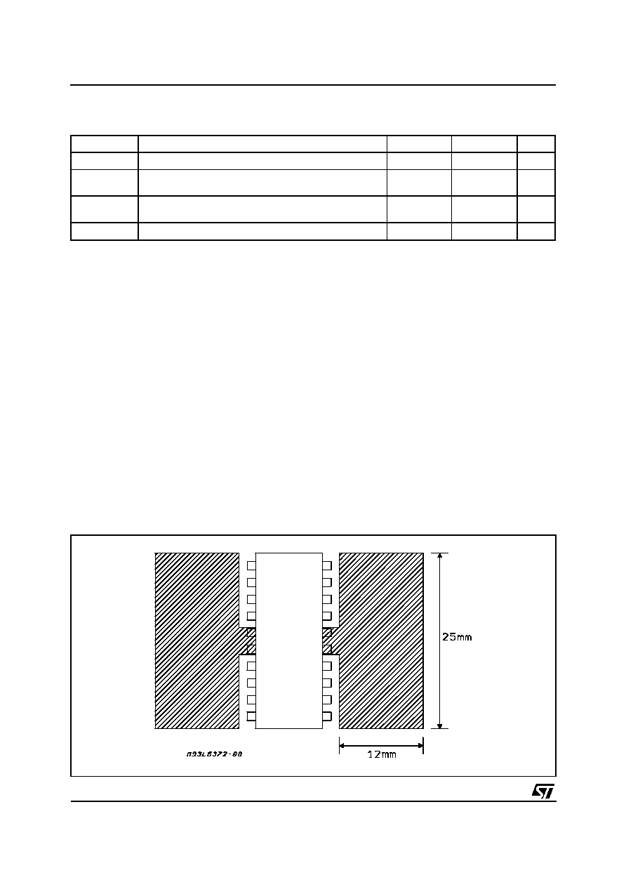
Figure 1: Printed Heatsink
L6376
6/12
OVERTEMPERATURE PROTECTION (OVT)
If the chip temperature exceeds
lim
(measured in
a central position in the chip) the chip deactivates
itself.
The following actions are taken:
∑
all the output stages are switched off;
∑
the signal DIAG is activated (active low).
Normal operation is resumed as soon as (typically
after some seconds) the chip temperature moni-
tored goes back below
lim
-
H
.
The different thresholds with hysteretic behavior
assure that no intermittent conditions can be gen-
erated.
UNDERVOLTAGE PROTECTION (UV)
The supply voltage is expected to range from
9.5V to 35V, even if its reference value is consid-
ered to be 24V.
In this range the device operates correctly.
Below 9.5V the overall system has to be consid-
ered not reliable.
Consequently the supply voltage is monitored
continuously and a signal, called UV, is internally
generated and used.
The signal is "on" as long as the supply voltage
does not reach the upper internal threshold of the
V
s
comparator V
sth
. The UV signal disappears
above V
sth
.
Once the UV signal has been removed, the sup-
ply voltage must decrease below the lower
threshold (i.e. V
sth
-V
shys
) before it is turned on
again.
The hysteresis V
shys
is provided to prevent inter-
mittent operation of the device at low supply volt-
ages that may have a superimposed ripple
around the average value.
The UV signal switches off the outputs, but has
no effect on the creation of the reference voltages
for the internal comparators, nor on the continu-
ous operation of the charge-pump circuits.
DIAGNOSTIC LOGIC
The situations that are monitored and signalled
with the DIAG output pin are:
∑
current limit (OVC) in action; there are 4 indi-
vidual current limiting circuits, one per each
output; they limit the current that can be sunk
from each output, to a typical value of
800mA, equal for all of them;
∑
under voltage (UV);
∑
over temperature protection (OVT).
The diagnostic signal is transmitted via an open
drain output (for ease of wired-or connection of
several such signals) and a low level represents
the presence of at least one of the monitored con-
ditions, mentioned above.
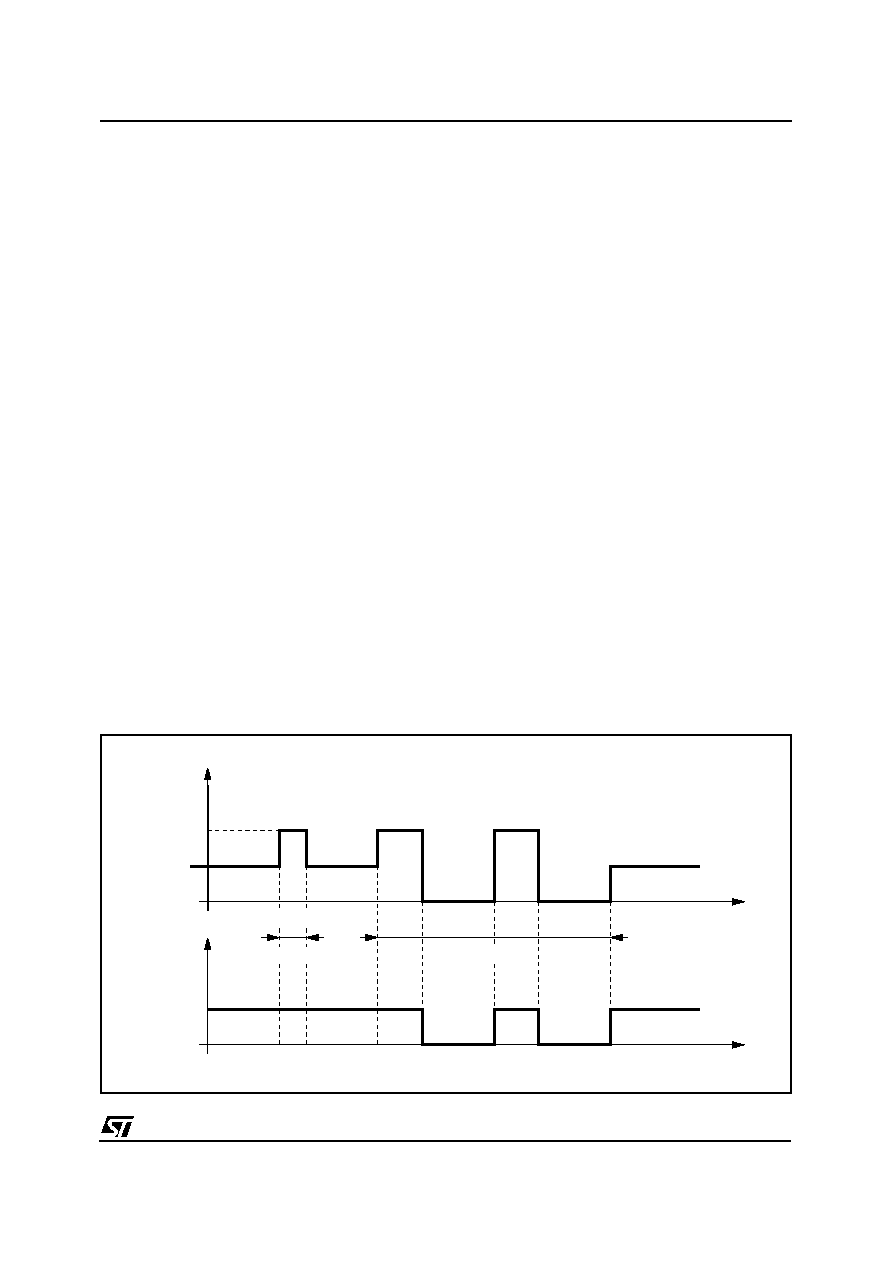
SHORT CIRCUIT OPERATION
In order to allow normal operation of the other in-
puts when one channel is in short cirtuit, an inno-
vative non dissipative over current protection (pat-
ent pending) is implemented in the device.
OUTPUT
CURRENT
t
ON
t
ON
t
OFF
t
OFF
Time
t<t
ON
DIAG
(active low)
Time
Short Circuit
Short Circuit
Isc
Iout
D94IN105
Figure 2: Short Circuit Operation Waveforms
L6376
7/12
In this way, the temperature of the device is kept
enough low to prevent the intervention of the ther-
mal protection (in most of the cases) and so to
avoid the shut down of the whole device.
If a short circuit condition is present on one out-
put, the current limiting circuit puts that channel in
linear mode -- sourcing the I
SC
current (typically
800 mA) -- for a time period (t
ON
) defined by an
external capacitor (C
DON
connected to the ON
DELAY pin).
After that period, if the short circuit condition is
still present the output is turned off for another
time period (t
OFF
) defined by a second external
capacitor (C
DOFF
connected to the OFF DELAY
pin).
When also this period is expired:
∑
if the short circuit condition is still present the
output stays on for the t
ON
period and the se-
quence starts again;
∑
if the short circuit condition is not present
anymore the normal operation of the output
is resumed.
The t
ON
and t
OFF
periods are completely inde-
pendent and can be set from 64
µ
s to 15 ms, us-
ing external capacitors ranging from 50 pF to
15 nF (1.28
µ
s/pF).
If the OFF DELAY pin is tied to ground (i.e. the
C
DOFF
capacitor is not used) the t
OFF
time period
is 64 times the t
ON
period.
The diagnostic output (DIAG) is active when the
output is switched off, while it is not active when
the output is on (i.e. during the t
ON
period) even if
in that period a short circuit condition is present.
Typical waveforms for short circuit operation are
shown in figure 2.
If both the ON DELAY and the OFF DELAY pins
are grounded the non dissipative over current
protection is inhibited and the outputs in short cir-
cuit remain on until the thermal shutdown switch
off the whole device. In this case the short circuit
condition is not signalled by the DIAG pin (that
continues to signal the under voltage and over
temperature conditions).
PROGRAMMABLE DIAGNOSTIC DELAY
The current limiting circuits can be requested to
perform even in absence of a real fault condition,
for a short period, if the load is of capacitive na-
ture or if it is a filament lamp (that exhibits a very
low resistance during the initial heating phase).
To avoid the forwarding of misleading -- i.e. short
diagnostic pulses in coincidence with the inter-
vention of the current limiting circuits when oper-
ating on capacitive loads -- the activation of the
diagnostic can be delayed with respect to the in-
tervention of one of the current limiting circuits.
This delay can be defined by an external capaci-
tor (C
DON
) connected between the ON DELAY pin
and ground.
RESET INPUT
An external reset input R (pin 18) is provided to
simultaneously switch off all the outputs: this sig-
nal (active low) is in effect an asynchronous reset
that keeps the outputs low independently from the
input signals.
For example, this reset input can be used by the
CPU to keep the outputs low after a fault condi-
tion (signaled by the DIAG pin).
DEMAGNETIZATION OF INDUCTIVE LOADS
The device has four internal clamping diodes able
to demagnetize inductive loads.
The limitation is the peak power dissipation of the
packages, so -- if the loads are big or if there is
the possibility to demagnetize more loads con-
temporarly -- it is necessary to use external de-
magnetization circuits.
In figures 4 and 5 are shown two topologies for
the demagnetization versus ground and versus
V
S
.
The breakdown voltage of the external device
(V
Z
) must be chosen considering the minimum in-
ternal clamping voltage (V
cl
) and the maximum
supply voltage (V
S
).
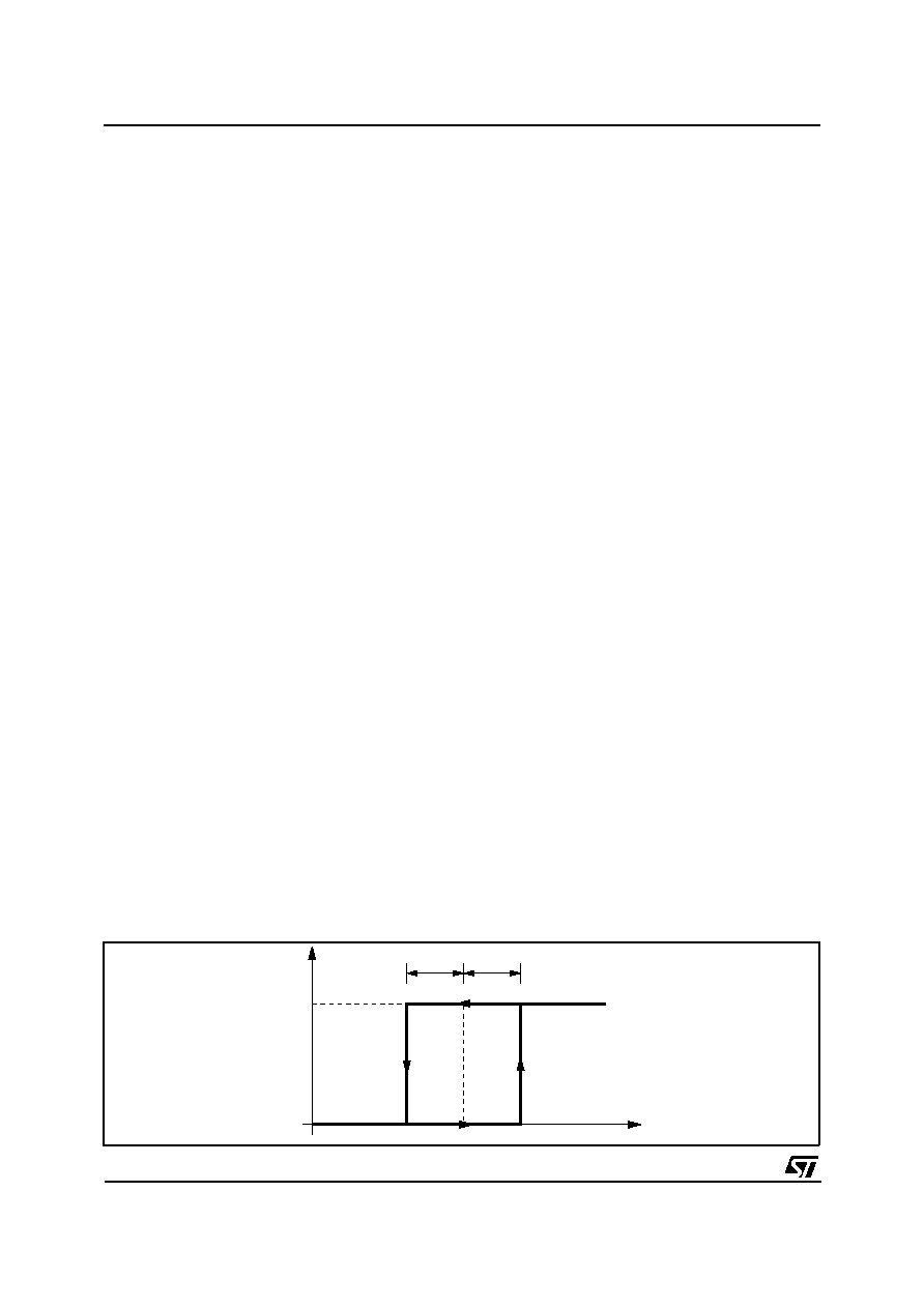
Vi
Vs
Vout
100mV
D94IN131
1.25V
100mV
Figure 3: Input Comparator Hysteresis
L6376
8/12
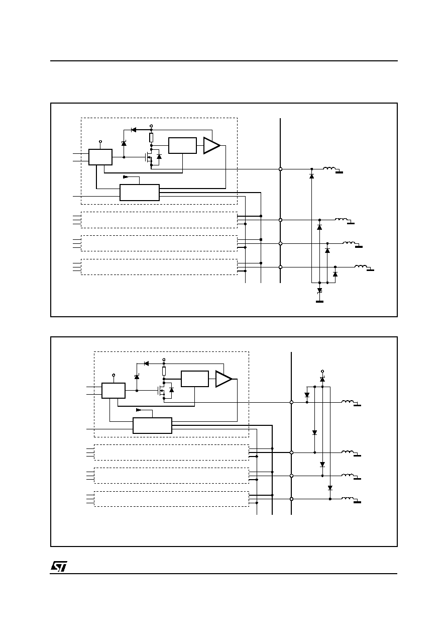
DRIVER
V
CP
V
S
OVC
O4
O3
O2
O1
D94IN110A
R
S
SHORT CIRCUIT
CONTROL
UV
CURRENT
LIMIT
V
Z
V
S (max)
<
V
Z
< V
cl (min)
V
S
Figure 5: External Demagnetization Circuit (versus V
S
)
DRIVER
VCP
VS
OVC
O4
O3
O2
O1
D94IN109
RS
SHORT CIRCUIT
CONTROL
UV
CURRENT
LIMIT
V
Z
V
Z
< V
cl (min)
- V
S (max)
Figure 4: External Demagnetization Circuit (versus ground)
L6376
9/12
DIM.
mm
inch
MIN.
TYP.
MAX.
MIN.
TYP.
MAX.
a1
0.51
0.020
B
0.85
1.40
0.033
0.055
b
0.50
0.020
b1
0.38
0.50
0.015
0.020
D
24.80
0.976
E
8.80
0.346
e
2.54
0.100
e3
22.86
0.900
F
7.10
0.280
I
5.10
0.201
L
3.30
0.130
Z
1.27
0.050
Powerdip 20
OUTLINE AND
MECHANICAL DATA
L6376
10/12
OUTLINE AND
MECHANICAL DATA
e
a2
A
E
a1
PSO20MEC
DETAIL A
T
D
1
10
11
20
E1
E2
h x 45
DETAIL A
lead
slug
a3
S
Gage Plane
0.35
L
DETAIL B
R
DETAIL B
(COPLANARITY)
G
C
- C -
SEATING PLANE
e3
b
c
N
N
H
BOTTOM VIEW
E3
D1
DIM.
mm
inch
MIN.
TYP.
MAX.
MIN.
TYP.
MAX.
A
3.6
0.142
a1
0.1
0.3
0.004
0.012
a2
3.3
0.130
a3
0
0.1
0.000
0.004
b
0.4
0.53
0.016
0.021
c
0.23
0.32
0.009
0.013
D (1)
15.8
16
0.622
0.630
D1
9.4
9.8
0.370
0.386
E
13.9
14.5
0.547
0.570
e
1.27
0.050
e3
11.43
0.450
E1 (1)
10.9
11.1
0.429
0.437
E2
2.9
0.114
E3
5.8
6.2
0.228
0.244
G
0
0.1
0.000
0.004
H
15.5
15.9
0.610
0.626
h
1.1
0.043
L
0.8
1.1
0.031
0.043
N
8∞ (typ.)
S
8∞ (max.)
T
10
0.394
(1) "D and E1" do not include mold flash or protusions.
- Mold flash or protusions shall not exceed 0.15mm (0.006")
- Critical dimensions: "E", "G" and "a3".
PowerSO20
0056635
JEDEC MO-166
Weight:
1.9gr
L6376
11/12

Information furnished is believed to be accurate and reliable. However, STMicroelectronics assumes no responsibility for the consequences
of use of such information nor for any infringement of patents or other rights of third parties which may result from its use. No license is
granted by implication or otherwise under any patent or patent rights of STMicroelectronics. Specifications mentioned in this publication are
subject to change without notice. This publication supersedes and replaces all information previously supplied. STMicroelectronics products
are not authorized for use as critical components in life support devices or systems without express written approval of STMicroelectronics.
The ST logo is a registered trademark of STMicroelectronics.
All other names are the property of their respective owners
© 2003 STMicroelectronics - All rights reserved
STMicroelectronics GROUP OF COMPANIES
Australia ≠ Belgium - Brazil - Canada - China ≠ Czech Republic - Finland - France - Germany - Hong Kong - India - Israel - Italy - Japan - Ma-
laysia - Malta - Morocco - Singapore - Spain - Sweden - Switzerland - United Kingdom - United States
www.st.com
L6376
12/12