 | –≠–ª–µ–∫—Ç—Ä–æ–Ω–Ω—ã–π –∫–æ–º–ø–æ–Ω–µ–Ω—Ç: L6377D | –°–∫–∞—á–∞—Ç—å:  PDF PDF  ZIP ZIP |
L6377
0.5A HIGH-SIDE DRIVER
INTELLIGENT POWER SWITCH
PRODUCT PREVIEW
0.5 A OUTPUT CURRENT
8 TO 35 V SUPPLY VOLTAGE RANGE
EXTERNALLY PROGRAMMABLE CURRENT
LIMIT
NON-DISSIPATIVE OVER-CURRENT PRO-
TECTION
THERMAL SHUTDOWN
UNDER VOLTAGE LOCKOUT WITH HYS-
TERESYS
DIAGNOSTIC OUTPUT FOR UNDER VOLT-
AGE, OVER TEMPERATURE AND OVER
CURRENT
EXTERNAL ASYNCHRONOUS RESET INPUT
PRESETTABLE DELAY
FOR
OVERCUR-
RENT DIAGNOSTIC
OPEN GROUND PROTECTION
PROTECTION
AGAINST
SURGE
TRAN-
SIENT (IEC 801-5)
IMMUNITY AGAINST BURST TRANSIENT
(IEC 801-4)
ESD PROTECTION (HUMAN BODY MODEL
±
2KV)
DESCRIPTION
This device is a monolithic Intelligent Power
Switch in Multipower BCD Technology for driving
inductive, capacitive or resistive loads.
Diagnostic for CPU feedback and extensive use
of electrical protections make this device inher-
ently indistructible and suitable for general pur-
pose industrial applications.
This is advanced information on a new product now in development or undergoing evaluation. Details are subject to change without notice.
February 1996
MINIDIP
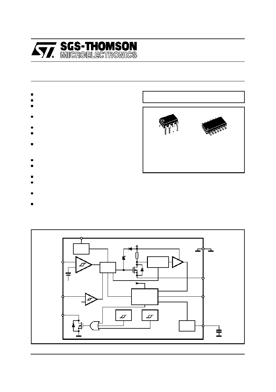
MULTIPOWER BCD TECHNOLOGY
DRIVER
+
-
VS
OVC
IN+
R
DIAG
OVT
UV
ON DELAY
C DON
OUT
GND
RS
SHORT CIRCUIT
CONTROL
DELAY
UV
CURRENT
LIMIT
VS
CHARGE
PUMP
D94IN075D
+
-
1.3V
1.3V
R
SC
BLOCK DIAGRAM
SO14
ORDERING NUMBERS: L6377 (MINIDIP)
L6377D (SO)
1/11
ABSOLUTE MAXIMUM RATINGS
Symbol
Pin
Parameter
Value
Unit
V
s
3
Supply Voltage (t
w
< 10ms)
50
V
Supply Voltage (DC)
40
V
V
s
- V
out
3 vs 2
Supply to Output Differential voltage
internally limited
V
od
5
Externally Forced Voltage
-0.3 to 7
V
I
od
Externally Forced Current
±
1
mA
I
RESET
4
Reset Input Current (forced)
±
2
mA
V
RESET
Reset Input Voltage
-0.3 to 40
V
I
out
2
Output Current (see also I
sc
)
internally limited
V
out
Output Voltage
internally limited
E
il
Total Energy Inductive Load (T
j
= 125
∞
C)
50
mJ
P
tot
Power Dissipation
internally limited
V
diag
6
External voltage
-0.3 to 40
V
I
diag
Externally forced current
-10 to 10
mA
I
i
7
Input Current
20
mA
V
i
Input Voltage
-10 to V
s
+0.3
V
T
op
Ambient temperature, operating range
-25 to 85
∞
C
T
j
Junction temperature, operating range (see
Overtemperature Protection)
-25 to 125
∞
C
T
stg
Storage temperature
-55 to 150
∞
C
PIN CONNECTION (Top view)
GND
OUT
V
S
R
SC
ON DELAY
DIAG
IN+
RESET
1
3
2
4
6
5
7
8
D94IN054D
N.C.
GND
OUT
V
S
R
SC
N.C.
N.C.
N.C.
ON DELAY
N.C.
DIAG
IN+
RESET
N.C.
1
3
2
4
5
6
7
12
11
10
9
8
13
14
D96IN368
L6377
2/11
PIN DESCRIPTION
No
Pins
Description
1
GND
Ground pin.
2
OUT
High side output. Controlled output with current limitation.
3
V
S
Supply voltage. Range with under voltage monitoring
4
Rsc
Current limiting setting.
5
ON DELAY
Delay setting for overcurrent diagnostic
6
DIAG
Diagnostic open drain output for over temperature, under voltage and overcurrent
7
IN+
Comparator non inverting input
8
RESET
Asynchronous reset input
THERMAL DATA
Symbol
Parameter
MINIDIP
SO14
Unit
R
th j-amb
Thermal Resistance, Junction Ambient
Max.
100
150
∞
C/W
L6377
3/11
ELECTRICAL CHARACTERISTICS (V
s
= 24V; T
j
= -25 to 125
∞
C; unless otherwise specified.)
DC OPERATION
Symbol
Pin
Parameter
Test Condition
Min.
Typ.
Max.
Unit
V
smin
3
Supply Voltage for Valid
Diagnostic
I
diag
= >0.5mA;
V
diag
= 1.5V;
4
35
V
V
s
Operative Supply Voltage
8
24
35
V
V
sth
Under Voltage Lower Threshold
7
8
V
V
shys
Under Voltage Hysteresis
300
500
700
mV
I
q
Quiescent Current
Output Open
800
µ
A
I
qo
Quiescent Current
Output On
1.6
mA
V
ith
7
Input Threshold Voltage
0.8
1.3
2
V
V
iths
Input Threshold Hysteresis
50
400
mV
V
il
Input Low Level Voltage
-7
0.8
V
V
ih
Input High Level Voltage
V
s
< 18V
2
V
s
-3
V
V
s
> 18V
2
15
V
I
ib
Input Bias Current
V
i
= -7 to 15V
-250
250
µ
A
V
rth
8
Reset Threshold Voltage
0.8
1.3
2
V
V
rl
Reset Low Level Voltage
0
0.8
V
V
rh
Reset High Level Voltage
2
40
V
I
rb
Reset Pull Down Current
5
µ
A
I
dch
5
Delay Capacitor Charging
Current
ON DELAY pin
shorted to Ground
2.5
µ
A
V
rsc
4
Output Voltage on R
sc
pin
R
sc
pin floating
1.25
V
I
rsc
Output Current on R
sc
pin
R
sc
pin shorted to GND
300
µ
A
I
dlkg
6
Diagnostic Output Leakage Curr.
Diagnostic Off
25
µ
A
V
diag
Diagnostic Output Voltage Drop
Idiag =5mA
;
1.5
V
V
don
2
Output Voltage Drop
I
out
=625mA
;
T
j
=25
∞
C
250
350
mV
I
out
=625mA
;
T
j
=125
∞
C
400
550
mV
I
olk
Output Leakage Current
V
i
= LOW; V
ou t
=0
100
µ
A
V
ol
Output Low State Voltage
V
i
= HIGH; pin floating
0.8
1.5
V
V
cl
Internal Voltage Clamp (V
s
-V
out
)
I
o
=200mA
single pulsed =300
µ
s
48
53
58
V
I
sc
Short Circuit Output Current
V
s
=8 to 35V; R
l
=2
;
R
sc
=5 to 30K
5/R
sc
= K
A
V
s
=8 to 35V; R
l
=2
;
R
sc
<5 K
0.75
1.1
1.5
A
T
max
Over Temperature Upper
Threshold
150
∞
C
T
hys
Over Temperature Hysteresis
20
∞
C
L6377
4/11
AC OPERATION
Symbol
Pin
Parameter
Test Condition
Min.
Typ.
Max.
Unit
t
r
-t
f
2
Rise or Fall Time
V
s
= 24V; R
l
= 70
R
l
to ground
20
µ
s
t
d
Delay Time
5
µ
s
dV/dt
Slew Rate (Rise and Fall
Edge)
V
s
= 24V; R
l
= 70
R
l
to ground
0.7
1
1.5
V/
µ
s
t
ON
5
On time during Short
Circuit Condition
50pF < C
DON
< 2nF
1.28
µ
s/pF
t
OFF
Off time during Short
Circuit Condition
64
t
ON
f
max
Maximum Operating
Frequency
25
kHz
SOURCE DRAIN NDMOS DIODE
Symbol
Parameter
Test Condition
Min.
Typ.
Max.
Unit
V
fsd
Forward On Voltage
I
fsd
= 625mA
1
1.5
V
I
fp
Forward Peak Current
t
p
= 10ms; duty cycle = 20%
1.5
A
t
rr
Reverse Recovery Time
I
fsd
= 500mA; dI
fsd
/dt = 25A/
µ
s
200
ns
t
fr
Forward Recovery Time
50
ns
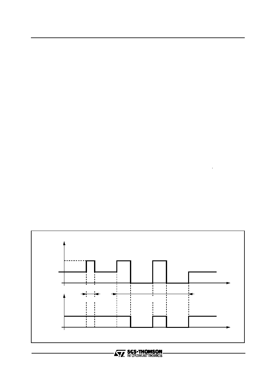
50%
50%
td
td
t
90%
90%
10%
10%
tf
tr
t
Vin
Vout
D94IN127A
50%
50%
Figure 2: Switching Waveforms
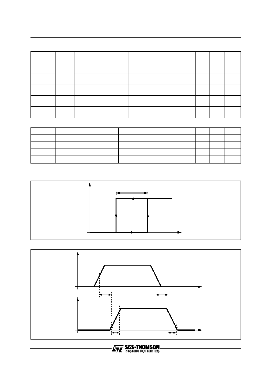
Vs
D94IN126A
Vsth
Vshys
Figure 1: Undervoltage Comparator Hysteresis
L6377
5/11
I
NPUT SECTION
An
Input
and
Asynchronous RESET,
both
TTL/CMOS compatible with wide voltage range
and high noise immunity (thanks to a built in hys-
teresis) are available.
OVER TEMPERATURE PROTECTION (OVT)
An on-chip Over Temperature Protection providse
an excellent protection of the device in extreme
conditions. Whenever the temperature - meas-
ured on a central portion of the chip- exceeds
Tmax=150 C (typical value) the device is shut off,
and the DIAG output goes LOW.
Normal operation is resumed as the chip tem-
perature (normally after few seconds) falls below
Tmax-Thys= 130 C (typical value). The hysteresis
avoid thats an intermittent behaviour take place.
UNDER VOLTAGE PROTECTION (UV)
The supply voltage is expected to range from 8 to
35 V. In this range the device operates correctly.
Below 8 V the overall system has to be consid-
ered not reliable. To avoid any misfunctioning the
supply voltage is continuously monitored to pro-
vide an under voltage protection. As Vs falls be-
low Vsth-Vshys (typically 7.5 V, see
fig.1) the
output power MOS is switched off and DIAG out-
put goes LOW. Normal operation is resumed as
soon as Vs exceeds Vsth. The hysteretic behav-
iour prevents intermittent operation at low supply
voltage.
OVER CURRENT OPERATION
In order to implement a short circuit protection the
output power MOS is driven in linear mode to limit
the output current to the Isc value. This Isc limit is
externally settable by means of an external 1/4 W
resistor connected from Rsc pin and GND. The
value of the resistor must be chosen according to
the following formula:
Isc (A) = 5/Rsc (kohm)
with
5 < Rsc < 30 (kohm)
For
Rsc < 5 (kohm)
Isc is limited to Isc=1.1 A (typical value).
This condition (current limited to the Isc value)
lasts for a Ton time interval, that can be set by
means of a capacitor (Cdon) connected to the ON
DELAY pin according to the following formula:
Ton = 1.28 msec/pF
for
50pF<Cdon< 2nF
After the Ton interval has expired the output
power MOS is switched off for the Toff time inter-
val with:
Toff = 64*Ton.
OUTPUT
CURRENT
t
ON
t
ON
t
OFF
t
OFF
Time
t<t
ON
DIAG
(active low)
Time
Short Circuit
Short Circuit
Isc
Iout
D94IN105
Figure 3: Short Circuit Operation Waveforms
L6377
6/11
When also the Toff interval has expired, the out-
put power MOS is switched ON.
Now two conditions may occur
- the overload is still present. In this case the out-
put power MOS is again driven in linear mode
(limiting the output current to Isc) for another Ton,
starting a new cycle, or
- the overload condition is removed, and the out-
put power MOS is no longer driven in linear
mode.
All these occurrences are presented on the DIAG
pin (see fig 2). We call this unique feature Non
Dissipative Short Circuit Protection and it en-
sures a very safe operation even in permanent
overload conditions. Note that, of course, choos-
ing the most appropriate value for the Ton interval
(i.e. the value of the Cdon capacitor) a delay (the
Ton itself) will prevent that a misleading Short Cir-
cuit information is presented on the DIAG output,
when driving capacitive loads (that acts like short
circuit in the very beginning) or Incandescent
Lamp (a cold filament has a very low resistive
value).
The Non Dissipative Short Circuit Protection can
be disabled (keeping Ton = 0 but with the output
current still limited to Isc, and Diagnostic dis-
abled) simply shorting to ground the the ON DE-
LAY pin.
DEMAGNETISATION OF INDUCTIVE LOADS
The L6377 has an internal clamping zener diode
able to demagnetise inductive loads. Note that
the limitation comes from the peak power that the
package can handle. Attention must be paid to a
proper thermal design of the board. If, for what-
ever reason (load current or inductive value too
big) the peak power dissipation is too high, an ex-
ternal Zener plus Diode arrangement, can per-
form a demagnetisation versus Ground or versus
Vs (see fig 5 and 6). The breakdown voltage of
the external Zener Diode must be chosen consid-
ering the internal clamping voltage (Vcl) and the
supply voltage (Vs) according to:
Vz< Vcl(min)-Vs(max)
for demagnetisation versus Ground or
Vs(max)<Vz<Vcl(min)
for demagnetisation versus Vs.
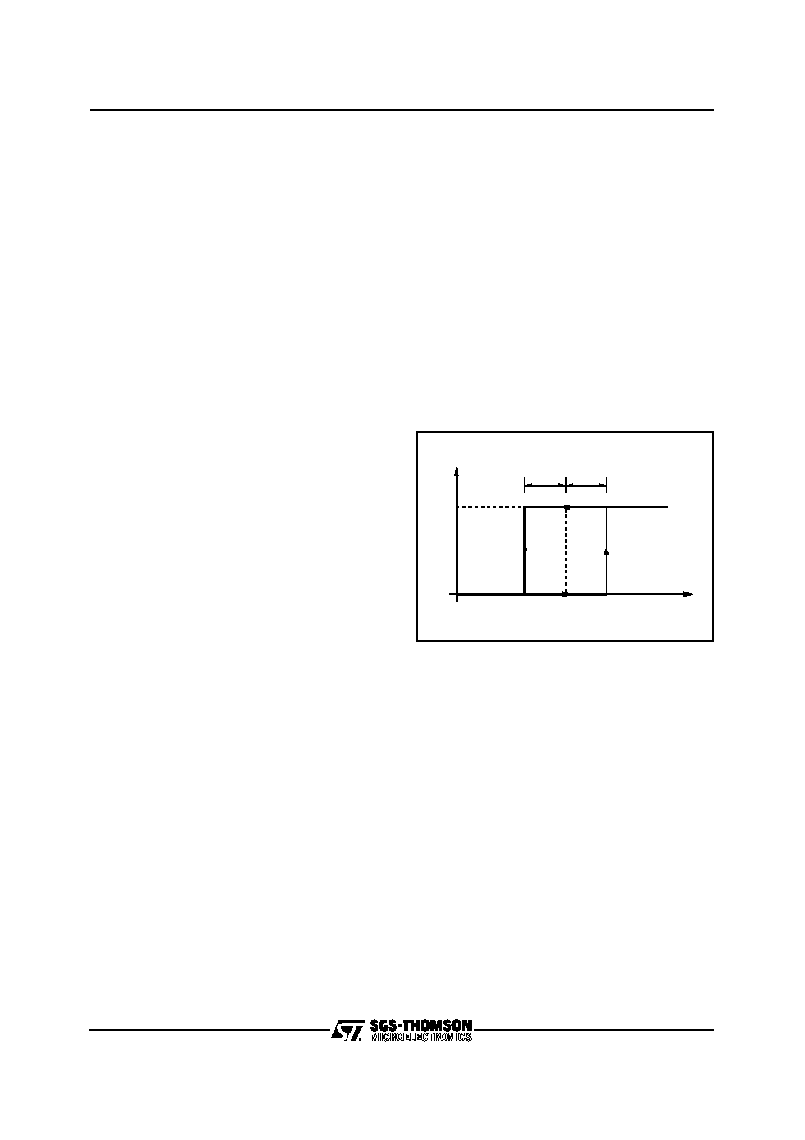
Vi+
Vs
Vout
100mV
D94IN079
Vi-
100mV
Figure 4: Input Comparator Hysteresis
L6377
7/11
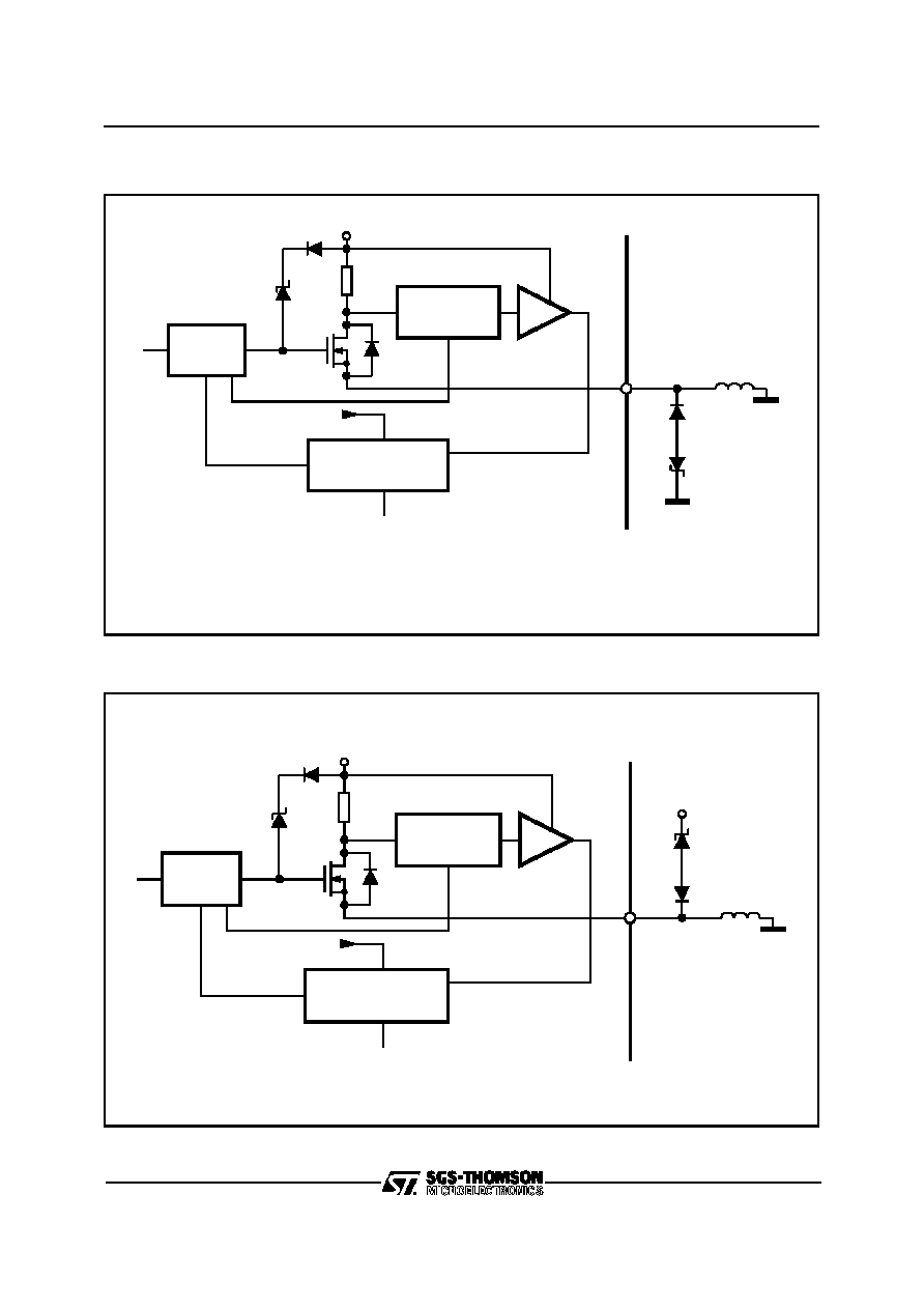
DRIVER
VS
OVC
OUT
RS
SHORT CIRCUIT
CONTROL
UV
CURRENT
LIMIT
D94IN111A
V
Z
V
S (max)
< V
Z
< V
cl (min)
V
S
Figure 6: External Demagnetisation Circuit (versus V
S
)
DRIVER
VS
OVC
OUT
RS
SHORT CIRCUIT
CONTROL
UV
CURRENT
LIMIT
D94IN112
V
Z
V
Z
< V
cl (min)
- V
S (max)
Figure 5: External Demagnetisation Circuit (versus ground)
L6377
8/11
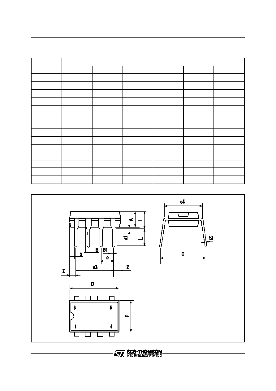
MINIDIP PACKAGE MECHANICAL DATA
DIM.
mm
inch
MIN.
TYP.
MAX.
MIN.
TYP.
MAX.
A
3.32
0.131
a1
0.51
0.020
B
1.15
1.65
0.045
0.065
b
0.356
0.55
0.014
0.022
b1
0.204
0.304
0.008
0.012
D
10.92
0.430
E
7.95
9.75
0.313
0.384
e
2.54
0.100
e3
7.62
0.300
e4
7.62
0.300
F
6.6
0.260
I
5.08
0.200
L
3.18
3.81
0.125
0.150
Z
1.52
0.060
L6377
9/11
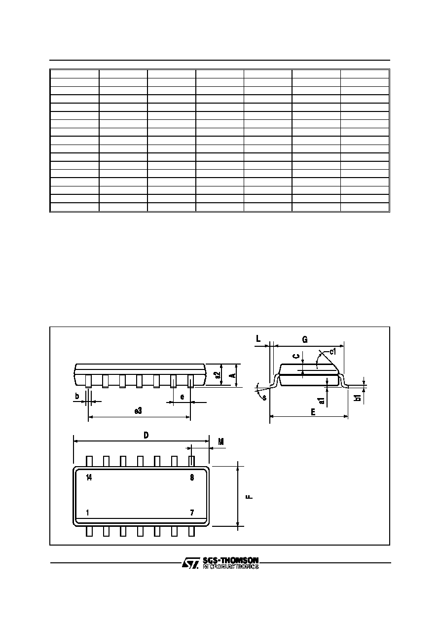
016019
MIN
TYP
MAX
MIN
TYP
MAX
A
1.75
0.069
a1
0.1
0.2
0.004
0.008
a2
1.6
0.063
b
0.35
0.46
0.014
0.018
b1
0.19
0.25
0.007
0.010
C
0.5
0.020
c1
45
1.772
D
1
8.55
0.039
0.337
E
5.8
6.2
0.228
0.244
e
1.27
0.050
e3
7.62
0.300
F
1
3.8
0.039
0.150
G
4.6
5.3
0.181
0.209
L
0.5
1.27
0.020
0.050
M
0.68
0.027
S
8
0.315
L6377
10/11

Information furnished is believed to be accurate and reliable. However, SGS-THOMSON Microelectronics assumes no responsibility for the
consequences of use of such information nor for any infringement of patents or other rights of third parties which may result from its use. No
license is granted by implication or otherwise under any patent or patent rights of SGS-THOMSON Microelectronics. Specification mentioned
in this publication are subject to change without notice. This publication supersedes and replaces all information previously supplied. SGS-
THOMSON Microelectronics products are not authorized for use as critical components in life support devices or systems without express
written approval of SGS-THOMSON Microelectronics.
©
1996 SGS-THOMSON Microelectronics ≠ Printed in Italy ≠ All Rights Reserved
SGS-THOMSON Microelectronics GROUP OF COMPANIES
Australia - Brazil - Canada - China - France - Germany - Hong Kong - Italy - Japan - Korea - Malaysia - Malta - Morocco - The Netherlands -
Singapore - Spain - Sweden - Switzerland - Taiwan - Thailand - United Kingdom - U.S.A.
L6377
11/11