 | –≠–ª–µ–∫—Ç—Ä–æ–Ω–Ω—ã–π –∫–æ–º–ø–æ–Ω–µ–Ω—Ç: L6506D | –°–∫–∞—á–∞—Ç—å:  PDF PDF  ZIP ZIP |
L6506
L6506D
June 1997
CURRENT CONTROLLER FOR STEPPING MOTORS
DESCRIPTION
The L6506/D is a linear integrated circuit designed
to sense and control the current in stepping motors
and similar devices. When used in conjunction with
the L293, L298, L7150, L6114/L6115, the chip set
forms a constant current drive for an inductive load
and performs all the interfacefunctionfrom the con-
trol logic thru the power stage.
Two or more devices may be synchronized using
the sync pin. In this mode of operation the oscillator
in the master chip sets the operating frequencyin all
chips.
DIP18
SO 20
ORDERING NUMBERS:
L6506
L6506D
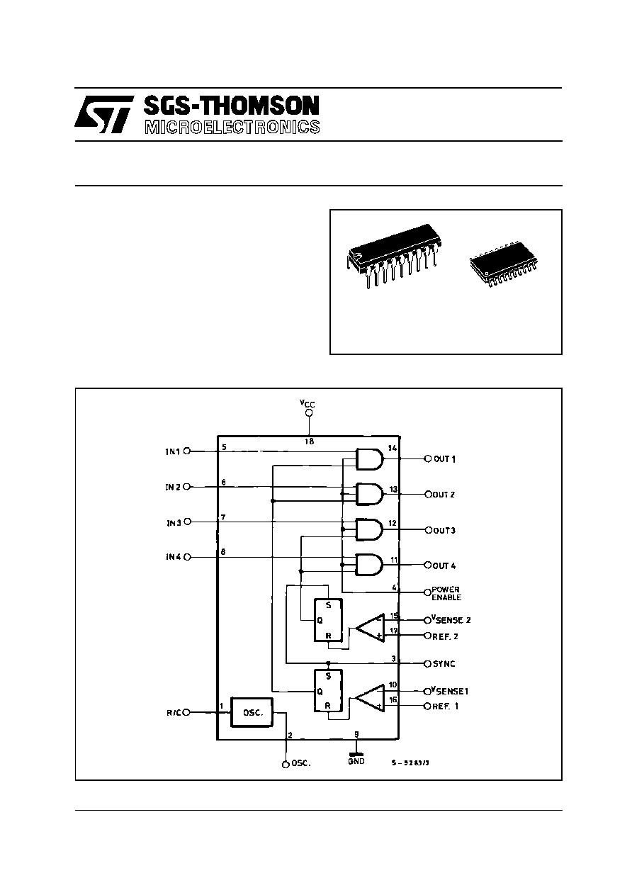
BLOCK DIAGRAM (pin's number referred to DIP-18)
1/8

PIN CONNECTIONS (top view)
ABSOLUTE MAXIMUM RATINGS
Symb ol
Parameter
Value
Un it
V
CC
Supply Voltage
10
V
V
i
Input Signals
7
V
P
tot
Total Power Dissipation (T
amb
= 70
∞
C) for DIP18
Total Power Dissipation (Tamb =70…C)
for SO20
1
0.8
W
W
T
j
Junction Temperature
150
∞
C
T
stg
Storage Temperature
-40 to 150
∞
C
THERMAL DATA
Symbol
Parameter
DIP18
SO20
Unit
R
th j-amb
Thermal Resistance Junction-ambient
Max.
80
100
∞
C/W
ELECTRICAL CHARACTERESTICS (V
CC
= 5.0V, T
amb
= 25
∞
C; unless otherwise noted)
Symbol
Parameter
T est Co ndi tio ns
Min.
T yp.
Max.
Un it
V
CC
Supply Voltage
4.5
7
V
I
CC
Quiescent Supply Current
V
CC
= 7V
25
mA
DIP 18
SO20
COMPARATOR SECTION
Symbol
Parameter
T est Co ndi tio ns
Min.
T yp.
Max.
Un it
V
IN
Input Voltage Range
V
sense
Inputs
≠0.3
3
V
V
IO
Input Offset Voltage
V
IN
= 1.4V
±
5.0
mV
I
IO
Input Offset Current
±
200
nA
I
IB
Input Bias Current
1
µ
A
Response time
V
REF
= 1.4V V
SENS
= 0 to 5V
0.8
1.5
µ
s
L6506 -L6506D
2/8

ELECTRICAL CHARACTERISTICS (continued)
COMPARATOR SECTION PERFORMANCE (Over Operating Temperature Range)
Symbol
Parameter
Test Condtions
Min.
Typ.
Max.
Unit
V
IO
Input Offset Voltage
V
IN
= 1.4V
±
20
mV
I
IO
Input Offset Curent
±
500
nA
CIRCUIT OPERATION
The L6506 is intended for use with dual bridge driv-
ers, such as the L298, quad darlington arrays, such
as the L7150, quad DMOS array such as L6114-
L6115,or discrete power transistors to drive stepper
motors and other similar loads.The main functionof
the device is to senseand control the current in each
of the load windings.
A commonon-chiposcillator drives thedual chopper
and sets the operatingfrequencyfor the pulse width
modulated drive. The RC network on pin 1 sets the
operating frequency which is given by the equation
:
1
f =
for R
>
10 K
0.69 RC
The oscillator provides pulses to set the two flip-
flops which in turn cause the outputs to activate the
drive. When the current in the load winding reaches
the programmed peak value, the voltage across the
sense resistor (R
sense
) is equal to V
ref
and the cor-
responding comparator resets its flip-flop interrupt-
ing the drive current untilthe next oscillatorpulse oc-
curs. The peak current in each winding is pro-
grammed by selecting the value of the sense resis-
tor and V
ref
. Since separate inputs are provided for
each chopper, each of the loads may be pro-
grammed independently allowing the device to be
used to implement microstepping of the motor.
Lower threshold of L6506'soscillator is 1/3 V
CC
. Up-
per threshold is 2/3 V
CC
and internal discharge re-
sistor is 1 K
±
30 %.
Ground noise problems in multiple configurations
can be avoided by synchronizing the oscillators.
This may be done by connecting the sync pins of
each of the devices with the oscillator output of the
master deviceand connectingthe R/C pin of the un-
used oscillators to ground.
The equations for the active time of the sync pulse
(T2), the inactivetime of the sync signal (T1)and the
dutycycle can be found by looking at the figure1 and
are :
R1 R
IN
T2 = 0.69 C1
(1)
R1 + R
IN
T1 = 0.69 R1 C1
(2)
T2
DC =
(3)
T1 + T2
LOGIC SECTION (Over Operating Temperature Range - TTL compatible inputs & outputs)
Symbol
Parameter
Test Condtions
Min.
Typ.
Max.
Unit
V
IH
Input High Voltage
2
V
s
V
V
IL
Input Low Voltage
0.8
V
V
OH
Output High Voltage
V
CC
= 4.75V
I
OH
= 400
µ
A
2
3.5
V
V
OL
Ouptut Low Voltage
V
CC
= 4.75V
I
OH
= 4mA
0.25
0.4
V
I
OH
Ouput Source Current - Outputs
1 - 4
V
CC
= 4.75V
2.75
mA
OSCILLATOR
Symbol
Parameter
Test Condtions
Min.
Typ.
Max.
Unit
f
osc
Frequency Range
5
70
KHz
V
thL
Lower Threshold Voltage
0.33 V
CC
V
V
thH
Higher Threshold Voltage
0.66 V
CC
V
R
i
Internal Discharge Resistor
0.7
1
1.3
k
L6506 - L6506D
3/8

By substituting equations 1 and 2 into equation 3
and solving for the value of R1 the following equa-
tions for the external components can be derived :
1
R1 = (
≠ 2) R
IN
(4)
DC
T1
C1 =
(5)
0.69 R1
Looking at equation 1 it can easily be seen that the
minimum pulse width of T2 will occur when the value
of R1 is at its minimum and the value of R1 at its
maximum. Therefore, when evaluating equation 4
the minimum value for R1 of 700
(1 K
≠ 30 %)
should be used to guarantee the required pulse
width.
Figure 1 : Oscillator Circuit and Waveforms.
APPLICATIONS INFORMATION
The circuits shown in figure 2 use the L6506 to im-
plement constant current drives for stepper motors.
Figure 2 shows the L6506 used with the L298 to
drive a 2 phasebipolar motor. The peak current can
be calculated using the equation :
V
ref
I
peak
=
R
sense
The circuit of Fig.2 can be used in applications re-
quiring different peak and hold current values by
modifying the reference voltage.
The L6506may be used to implement eitherfull step
or half step drives. In the case of 2 phase bipolar
stepper motor applications, if a half step drive is
used, the bridge requires an additional input to dis-
able the power stage during the half step. If used in
conjunction with the L298 the enable inputs may be
used for this purpose.
For quad darlington array in 4 phase unipolar motor
applications half step may be implemented using
the 4 phase inputs.
The L6506 may also be used to implement mi-
crostepping of either bipolar or unipolar motors.
L6506 -L6506D
4/8

Figure 2 : Application Circuit Bipolar Stepper Motor Driver. (pin's number referred to DIP18)
L6506 - L6506D
5/8