 | –≠–ª–µ–∫—Ç—Ä–æ–Ω–Ω—ã–π –∫–æ–º–ø–æ–Ω–µ–Ω—Ç: L6710 | –°–∫–∞—á–∞—Ç—å:  PDF PDF  ZIP ZIP |

1/34
L6710
March 2004
2 PHASE OPERATION WITH
SYNCRHONOUS RECTIFIER CONTROL
ULTRA FAST LOAD TRANSIENT RESPONSE
INTEGRATED HIGH CURRENT GATE
DRIVERS: UP TO 2A GATE CURRENT
6 BIT PROGRAMMABLE OUTPUT
COMPLIANT WITH VRD 10
DYNAMIC VID MANAGEMENT
0.5% OUTPUT VOLTAGE ACCURACY
10% ACTIVE CURRENT SHARING
ACCURACY
DIGITAL 2048 STEP SOFT-START
OVERVOLTAGE PROTECTION
OVERCURRENT PROTECTION REALIZED
USING THE LOWER MOSFET'S R
dsON
OR A
SENSE RESISTOR
OSCILLATOR EXTERNALLY ADJUSTABLE
AND INTERNALLY FIXED AT 150kHz
POWER GOOD OUTPUT AND ENABLE
FUNCTION
INTEGRATED REMOTE SENSE BUFFER
APPLICATIONS
POWER SUPPLY FOR HIGH CURRENT
MICROPROCESSORS
POWER SUPPLY FOR SERVER AND
WORKSTATION
DISTRIBUTED POWER SUPPLY
DESCRIPTION
The device implements a two phase step-down
controller with a 180 phase-shift between each
phase with integrated high current drivers in a
compact 10x10mm body package with exposed
pad. A precise 6-bit digital to analog converter
(DAC) allows adjusting the output voltage from
0.8375V to 1.6000V with 12.5mV binary steps
managing Dynamic VID code changes.
The high precision internal reference assures the
selected output voltage to be within 0.5% over line
and temperature variations. The high peak current
gate drive affords to have fast switching to the ex-
ternal power mos providing low switching losses.
The device assures a fast protection against load
over current and load over/under voltage. An inter-
nal crowbar is provided turning on the low side
mosfet if an over-voltage is detected.
In case of over-current, the system works in Con-
stant Current mode until UVP
PIN CONNECTION (top view)
REF_OUT
VSEN
OUTEN
N.C.
N.C.
FBR
FBG
ISEN1
PGNDS
ISEN2
OSC / FAULT
N.C.
HGATE1
PHASE1
VCCDR
LGATE1
PGND
LGATE2
N.C.
PHASE2
HGATE2
N.C.
N.
C.
VI
D0
VI
D1
VI
D2
VI
D3
VI
D4
VI
D5
PG
O
O
D
BO
O
T
2
N.
C.
N.
C.
N.C
.
N.C
.
BO
O
T
1
N.C
.
VCC
SG
ND
SG
ND
COM
P
FB
N.C
.
N.C
.
34
35
36
37
38
39
40
41
42
43
1
44
2
3
4
5
6
7
8
9
10 11
22
21
20
19
18
17
16
15
14
13
12
33 32 31 30 29 28 27 26 25 24 23
TQFP44 (10 x 10 x 1mm) Exposed Pad
ORDERING NUMBERS:L6710
L6710TR (Tape & Reel)
6 BIT PROGRAMMABLE DUAL-PHASE CONTROLLER
WITH DYNAMIC VID MANAGEMENT

L6710
2/34
BLOCK DIAGRAM
ABSOLUTE MAXIMUM RATINGS
THERMAL DATA
Symbol
Parameter
Value
Unit
Vcc, V
CCDR
To PGND
15
V
V
BOOT
-V
PHASE
Boot Voltage
15
V
V
UGATE1
-V
PHASE1
V
UGATE2
-V
PHASE2
15
V
LGATE1, PHASE1, LGATE2, PHASE2 to PGND
-0.3 to Vcc+0.3
V
VID0 to VID5
-0.3 to 5
V
All other pins to PGND
-0.3 to 7
V
V
PHASEx
Sustainable Peak Voltage. T<20nS @ 600kHz
26
V
Symbol
Parameter
Value
Unit
R
th j-amb
Thermal Resistance Junction to Ambient
40
∞C/W
T
max
Maximum junction temperature
150
∞C
T
stg
Storage temperature range
-40 to 150
∞C
T
j
Junction Temperature Range
0 to 125
∞C
P
MAX
Max power dissipation at Tamb=25
∞C
2.5
W
CURRENT
READING
I
FB
TO TAL
CURRENT
CU
RR
E
N
T
AVG
CH1
OCP
DAC
DIGITAL
SOFT-START
LO
G
I
C
P
W
M
AD
AP
T
I
VE
AN
T
I
C
R
OS
S
C
O
N
D
U
C
T
I
ON
CH1 OCP
2
PH
A
S
E
OS
C
I
L
L
A
T
OR
PWM1
CU
RR
E
N
T
CO
RR
E
C
T
I
O
N
ERROR
AMPL IFIER
REMOTE
BUFFER
32k
32k
32k
LS
LS
HS
Vcc
HS
BOOT1
U
GATE1
PHASE1
LGATE1
ISEN1
PGND
PGNDS
ISEN2
LGATE2
PHASE2
UGATE2
BOOT2
Vcc
COMP
FB
FBG
FBR
VID1
VID2
VID3
VID4
VID5
PGOOD
OSC / FAULT
SGND
VCCDR
32k
VCCDR
VCC
L
O
G
I
C A
ND
P
R
OT
E
C
T
I
ON
S
CH2 OCP
PWM2
CU
RR
E
N
T
CO
RR
E
C
T
I
O
N
CH2
OCP
CURRENT
READING
LO
G
I
C
P
W
M
AD
A
P
T
I
VE
AN
T
I
CR
O
S
S
CO
ND
U
C
T
I
O
N
VID0
OUTEN
REF_OUT
VSEN
CURRENT
READING
CURRENT
READING
I
FB
TO TAL
CURRENT
CU
RR
E
N
T
AVG
CH1
OCP
DAC
DIGITAL
SOFT-START
LO
G
I
C
P
W
M
AD
AP
T
I
VE
AN
T
I
C
R
OS
S
C
O
N
D
U
C
T
I
ON
LO
G
I
C
P
W
M
AD
AP
T
I
VE
AN
T
I
C
R
OS
S
C
O
N
D
U
C
T
I
ON
CH1 OCP
2
PH
A
S
E
OS
C
I
L
L
A
T
OR
PWM1
CU
RR
E
N
T
CO
RR
E
C
T
I
O
N
ERROR
AMPL IFIER
REMOTE
BUFFER
32k
32k
32k
LS
LS
HS
Vcc
HS
BOOT1
U
GATE1
PHASE1
LGATE1
ISEN1
PGND
PGNDS
ISEN2
LGATE2
PHASE2
UGATE2
BOOT2
Vcc
COMP
FB
FBG
FBR
VID1
VID2
VID3
VID4
VID5
PGOOD
OSC / FAULT
SGND
VCCDR
32k
VCCDR
VCC
L
O
G
I
C A
ND
P
R
OT
E
C
T
I
ON
S
CH2 OCP
PWM2
CU
RR
E
N
T
CO
RR
E
C
T
I
O
N
CH2
OCP
CURRENT
READING
CURRENT
READING
LO
G
I
C
P
W
M
AD
A
P
T
I
VE
AN
T
I
CR
O
S
S
CO
ND
U
C
T
I
O
N
LO
G
I
C
P
W
M
AD
A
P
T
I
VE
AN
T
I
CR
O
S
S
CO
ND
U
C
T
I
O
N
VID0
OUTEN
REF_OUT
VSEN

3/34
L6710
PIN FUNCTION
N
Name
Description
1
N.C.
Not internally bonded.
2
N.C.
Not internally bonded.
3
BOOT1
Channel 1 HS driver supply. This pin supplies the relative high side driver.
Connect through a capacitor (100nF typ.) to the PHASE1 pin and through a diode to VCC
(cathode vs. boot).
4
N.C.
Not internally bonded.
5
VCC
Device supply voltage. The operative supply voltage is 12V ±15%.
Filter with 1
µF (Typ.) capacitor vs. GND.
6,7
SGND
All the internal references are referred to this pin. Connect it to the PCB signal ground.
8
COMP
This pin is connected to the error amplifier output and is used to compensate the control
feedback loop.
9
FB
This pin is connected to the error amplifier inverting input and is used to compensate the
voltage control feedback loop.
A current proportional to the sum of the current sensed in both channel is sourced from this
pin (50
µA at full load, 70µA at the Constant Current threshold). Connecting a resistor
between this pin and VSEN pin allows programming the droop effect.
10,11
N.C.
Not internally bonded.
12
REF_OUT
Reference voltage output used for voltage regulation.
The pin is protected against short circuit vs. ground.
Filter to SGND with 47nF ceramic capacitor.
13
VSEN
Manages Over&Under-voltage conditions and the PGOOD signal. It is internally connected
with the output of the Remote Sense Buffer for Remote Sense of the regulated voltage.
If no Remote Sense is implemented, connect it directly to the regulated voltage in order to
manage OVP, UVP and PGOOD.
Connecting 1nF capacitor max vs. SGND can help in reducing noise injection.
14
OUTEN
Output Enable pin. Internally 3V pulled-up.
If forced to a voltage lower than 0.4V, the device stops operation with all mosfets and
protections OFF. Setting the pin free, the device re-start operations.
Filter with 1nF capacitor vs. SGND to avoid noise injection.
15, 16
N.C.
Not internally bonded.
17
FBR
Remote sense buffer non-inverting input. It has to be connected to the positive side of the
load to perform a remote sense.
If no remote sense is implemented, connect directly to the output voltage (in this case
connect also the VSEN pin directly to the output regulated voltage).
18
FBG
Remote sense buffer inverting input. It has to be connected to the negative side of the load
to perform a remote sense.
Pull-down to ground if no remote sense is implemented.
19
ISEN1
Channel 1 current sense pin. The output current may be sensed across a sense resistor or
across the low-side mosfet R
dsON.
This pin has to be connected to the low-side mosfet drain
or to the sense resistor through a resistor Rg.
The net connecting the pin to the sense point must be routed as close as possible to the
PGNDS net in order to couple in common mode any picked-up noise.
20
PGNDS
Common Power Ground sense pin. The net connecting the pin to the sense point must be
routed as close as possible to the ISENx net in order to couple in common mode any picked-
up noise.
21
ISEN2
Channel 2 current sense pin. The output current may be sensed across a sense resistor or
across the low-side mosfet R
dsON.
This pin has to be connected to the low-side mosfet drain
or to the sense resistor through a resistor Rg.
The net connecting the pin to the sense point must be routed as close as possible to the
PGNDS net in order to couple in common mode any picked-up noise.

L6710
4/34
22
OSC/FAULT
Oscillator pin.
It allows programming the switching frequency of each channel: the equivalent switching
frequency at the load side results in being doubled.
Internally fixed at 1.24V, the frequency is varied proportionally to the current sunk (forced)
from (into) the pin with an internal gain of 6kHz/
µA (See relevant section for details). If the
pin is not connected, the switching frequency is 150kHz for each channel (300kHz on the
load).
The pin is forced high (5V Typ.) when an Over/Under Voltage is detected; to recover from
these latched conditions, cycle VCC.
23
N.C.
Not internally bonded.
24 to 29
VID0-5
Voltage IDentification pins.
Internally pulled-up, connect to SGND to program a `0' while leave floating to program a `1'.
They are used to program the output voltage as specified in Table 1 and to set the PGOOD,
OVP and UVP thresholds.
Since the VID pins program the maximum output voltage, according to VRD10 specs, the
device automatically regulates to a voltage VID* = VID≠25mV avoiding use of any external
component to lower the regulated voltage.
30
PGOOD
This pin is an open collector output and is pulled low if the output voltage is not within the
above-specified thresholds and during soft-start. It cannot be pulled up above 3.3V
If not used may be left floating.
31
BOOT2
Channel 2 HS driver supply. This pin supplies the relative high side driver.
Connect through a capacitor (100nF typ.) to the PHASE2 pin and through a diode to VCC
(cathode vs. boot).
32 to 34
N.C.
Not internally bonded.
35
HGATE2
Channel 2 HS driver output.
A little series resistor helps in reducing device-dissipated power.
36
PHASE2
Channel 2 HS driver return path. It must be connected to the HS2 mosfet source and
provides the return path for the HS driver of channel 2.
37
N.C.
Not internally bonded.
38
LGATE2
Channel 2 LS driver output.
A little series resistor helps in reducing device-dissipated power.
39
PGND
LS drivers return path.
This pin is common to both sections and it must be connected through the closest path to
the LS mosfets source pins in order to reduce the noise injection into the device.
40
LGATE1
Channel 1 LS driver output.
A little series resistor helps in reducing device-dissipated power.
41
VCCDR
LS drivers supply: it can be varied from 5V to 12V buses.
Filter locally with at least 1
µF ceramic cap vs. PGND.
42
PHASE1
Channel 1 HS driver return path. It must be connected to the HS1 mosfet source and
provides the return path for the HS driver of channel 1.
43
HGATE1
Channel 1 HS driver output.
A little series resistor helps in reducing device-dissipated power.
44
N.C.
Not internally bonded.
PAD
THERMAL
PAD
Thermal pad connects the silicon substrate and makes a good thermal contact with the PCB
to dissipate the power necessary to drive external mosfets. Connect to the GND plane with
several vias to improve thermal conduction.
PIN FUNCTION (continued)
N
Name
Description

5/34
L6710
ELECTRICAL CHARACTERISTICS
(V
cc
= 12V±15%, T
J
= 0 to 70∞C unless otherwise specified)
Symbol
Parameter
Test Condition
Min
Typ
Max
Unit
Vcc SUPPLY CURRENT
I
CC
Vcc supply current
HGATEx and LGATEx open
VCCDR=BOOT=12V
7.5
10
12.5
mA
I
CCDR
V
CCDR
supply current
LGATEx open; VCCDR=12V
2
3
4
mA
I
BOOTx
Boot supply current
HGATEx open; PHASEx to
PGND
VCC=BOOTx=12V
0.5
1
1.5
mA
POWER-ON
Turn-On V
CC
threshold
VCC Rising; VCCDR=5V
8.2
9.2
10.2
V
Turn-Off V
CC
threshold
VCC Falling; VCCDR=5V
6.5
7.5
8.5
V
Turn-On V
CCDR
Threshold
VCCDR Rising
VCC=12V
4.2
4.4
4.6
V
Turn-Off V
CCDR
Threshold
VCCDR Falling
VCC=12V
4.0
4.2
4.4
V
OUTEN
IL
Output Enable
Level
Input Low
0.4
V
OUTEN
IH
Input High
0.8
V
OSCILLATOR
f
OSC
Initial Accuracy
OSC = OPEN
OSC = OPEN; Tj=0
∞C to 125∞C
135
127
150
165
178
kHz
kHz
d
MAX
Maximum duty cycle
OSC = OPEN: I
FB
=0
OSC = OPEN; I
FB
=70
µA
72
30
80
40
%
%
Vosc
Ramp Amplitude
3
V
FAULT
Voltage at pin OSC
OVP or UVP Active
4.75
5.0
5.25
V
REFERENCE AND DAC
Output Voltage
Accuracy
VID0 to VID5 see Table1;
FBR = V
OUT
; FBG = GND
-0.5
-
0.5
%
REF_OUT
REF_OUT Accuracy
VID0 to VID5 see Table1;
-1.5
-
1.5
%
I
VID
VID pull-up Current
VIDx = GND
3
4.5
6
µA
V
VID
VID pull-up Voltage
VIDx = OPEN
2.9
-
3.3
V
VID
IL
VID Input
Level
Input Low
0.4
V
VID
IH
Input High
1.0
V
ERROR AMPLIFIER
A
0
DC Gain
80
dB
SR
Slew-Rate
COMP=10pF
15
V/
µs

L6710
6/34
DIFFERENTIAL AMPLIFIER (REMOTE BUFFER)
DC Gain
1
V/V
CMRR
Common Mode Rejection Ratio
40
dB
SR
Slew Rate
VSEN=10pF
15
V/
µs
DIFFERENTIAL CURRENT SENSING
I
ISEN1
,
I
ISEN2
Bias Current
I
LOAD
=0%
45
50
55
µA
I
PGNDSx
Bias Current
45
50
55
µA
I
ISEN1
,
I
ISEN2
Bias Current at
Over Current Threshold
80
85
90
µA
I
FB
Active Droop Current
I
LOAD
=0
0
1
µA
I
LOAD
=100%
47.5
50
52.5
µA
GATE DRIVERS
t
RISE
HGATE
High Side Rise Time
BOOTx-PHASEx=10V;
HGATEx to PHASEx=3.3nF
15
30
ns
I
HGATEx
High Side Source Current
BOOTx-PHASEx=10V
2
A
R
HGATEx
High Side Sink Resistance
BOOTx-PHASEx=10V;
1.8
2.5
t
RISE
LGATE
Low Side Rise Time
VCCDR=10V;
LGATEx to PGND=5.6nF
30
55
nS
I
LGATEx
Low Side Source Current
VCCDR=10V
1.8
A
R
LGATEx
Low Side Sink Resistance
VCCDR=10V
1.1
1.5
PROTECTIONS
PGOOD
Upper Threshold
(VSEN
/ DAC Output)
VSEN Rising
108
112
116
%
PGOOD
Lower Threshold
(VSEN
/ DAC Output)
VSEN Falling
84
88
92
%
OVP
Over Voltage Threshold
(VSEN
/ DAC Output)
VSEN Rising
122
126
130
%
UVP
Under Voltage Trip
(VSEN
/ DAC Output)
VSEN Falling
55
60
65
%
V
PGOODL
PGOOD Voltage Low
I
PGOOD
= -4mA
0.4
V
I
PGOODH
PGOOD VLeakage
V
PGOOD
= 3.3V
1
µA
ELECTRICAL CHARACTERISTICS (continued)
(V
cc
= 12V±15%, T
J
= 0 to 70∞C unless otherwise specified)
Symbol
Parameter
Test Condition
Min
Typ
Max
Unit

7/34
L6710
Table 1. Voltage IDentification (VID) Codes.
(*) Since the VID pins program the maximum output voltage, according to VRD 10.0 specs, the device automatically regulate to a voltage
VID*=VID-25mV avoiding use of any external component to lower the regulated voltage.
VID5
VID4 VID3
VID2
VID1
VID0
Output
Voltage
(V) (*)
VID5
VID4 VID3
VID2
VID1
VID0
Output
Voltage
(V) (*)
0
0
1
0
1
0
0.8375
0
1
1
0
1
0
1.2125
1
0
1
0
0
1
0.8500
1
1
1
0
0
1
1.2250
0
0
1
0
0
1
0.8625
0
1
1
0
0
1
1.2375
1
0
1
0
0
0
0.8750
1
1
1
0
0
0
1.2500
0
0
1
0
0
0
0.8875
0
1
1
0
0
0
1.2625
1
0
0
1
1
1
0.9000
1
1
0
1
1
1
1.2750
0
0
0
1
1
1
0.9125
0
1
0
1
1
1
1.2875
1
0
0
1
1
0
0.9250
1
1
0
1
1
0
1.3000
0
0
0
1
1
0
0.9375
0
1
0
1
1
0
1.3125
1
0
0
1
0
1
0.9500
1
1
0
1
0
1
1.3250
0
0
0
1
0
1
0.9625
0
1
0
1
0
1
1.3375
1
0
0
1
0
0
0.9750
1
1
0
1
0
0
1.3500
0
0
0
1
0
0
0.9875
0
1
0
1
0
0
1.3625
1
0
0
0
1
1
1.0000
1
1
0
0
1
1
1.3750
0
0
0
0
1
1
1.0125
0
1
0
0
1
1
1.3875
1
0
0
0
1
0
1.0250
1
1
0
0
1
0
1.4000
0
0
0
0
1
0
1.0375
0
1
0
0
1
0
1.4125
1
0
0
0
0
1
1.0500
1
1
0
0
0
1
1.4250
0
0
0
0
0
1
1.0625
0
1
0
0
0
1
1.4375
1
0
0
0
0
0
1.0750
1
1
0
0
0
0
1.4500
0
0
0
0
0
0
1.0875
0
1
0
0
0
0
1.4625
1
1
1
1
1
1
OFF
1
0
1
1
1
1
1.4750
0
1
1
1
1
1
OFF
0
0
1
1
1
1
1.4875
1
1
1
1
1
0
1.1000
1
0
1
1
1
0
1.5000
0
1
1
1
1
0
1.1125
0
0
1
1
1
0
1.5125
1
1
1
1
0
1
1.1250
1
0
1
1
0
1
1.5250
0
1
1
1
0
1
1.1375
0
0
1
1
0
1
1.5375
1
1
1
1
0
0
1.1500
1
0
1
1
0
0
1.5500
0
1
1
1
0
0
1.1625
0
0
1
1
0
0
1.5625
1
1
1
0
1
1
1.1750
1
0
1
0
1
1
1.5750
0
1
1
0
1
1
1.1875
0
0
1
0
1
1
1.5875
1
1
1
0
1
0
1.2000
1
0
1
0
1
0
1.6000

L6710
8/34
REFERENCE SCHEMATIC
DEVICE DESCRIPTION
The device is an integrated circuit realized in BCD technology. It provides complete control logic and pro-
tections for a high performance dual-phase step-down DC-DC converter optimized for microprocessor
power supply. It is designed to drive N Channel MOSFETs in a two-phase synchronous-rectified buck to-
pology. A 180 deg phase shift is provided between the two phases allowing reduction in the input capacitor
current ripple, reducing also the size and the losses.
The output voltage of the converter can be precisely regulated, programming the VID pins, from 0.8375 to
1.6000V with 12.5mV binary steps, with a maximum tolerance on the output regulated voltage of ±0.5%
over temperature and line voltage variations. Since the VID pins program the maximum output voltage,
the device automatically regulates to a voltage VID*=VID-25mV avoiding use of any external component
to lower the regulated voltage. Dynamic VID Code changes are managed stepping to the new configura-
tion following the VID table with no need for external components. The device provides an average cur-
rent-mode control with fast transient response. It includes a 150kHz oscillator externally adjustable
through a resistor. The error amplifier features a 15V/
µs slew rate that permits high converter bandwidth
for fast transient performances.
Current information is read across the lower mosfets R
dsON
or across a sense resistor placed in series to
the LS mos in fully differential mode. The current information corrects the PWM output in order to equalize
the average current carried by each phase. Current sharing between the two phases is then limited at
±10% over static and dynamic conditions unless considering the sensing element spread.
The device protects against Over-Current, with an OC threshold for each phase, entering in constant cur-
rent mode. Since the current is read across the low side mosfets, the device keeps constant the bottom
of the inductors current triangular waveform. When an under voltage is detected the device latches and
the FAULT pin is driven high. The device performs also Over-Voltage protection that disables immediately
the device turning ON the lower driver and driving high the FAULT pin.
L6710
PGOOD
PGND
PGNDS
ISEN2
LGATE2
VSEN
FB
PHASE2
HGATE2
BOOT2
VCC
COMP
SGND
REF_OUT
VID0
VID1
VID2
VID3
VID4
To PGNDS
ISEN1
LGATE1
PHASE1
HGATE1
BOOT1
VCCDR
5
31
35
36
38
21
20
41
3
43
42
40
19
28
27
26
24
25
6, 7
39
30
13
9
8
14
18
OUTEN
FBG
12
R
FB
R
F
C
F
Rg
Rg
LS2
HS2
L2
C
IN
C
OUT
S1
S0
S3
S2
S4
Rg
LS1
L1
HS1
Vin
GNDin
PGOOD
CPU
Rg
VID5
29
S5
OSC / FAULT
22
17
FBR
VID_Pgood
To VCC

9/34
L6710
OSCILLATOR
The switching frequency is internally fixed at 150kHz. Each phase works at the frequency fixed by the os-
cillator so that the resulting switching frequency at the load side results in being doubled.
The internal oscillator generates the triangular waveform for the PWM charging and discharging with a
constant current an internal capacitor. The current delivered to the oscillator is typically 25
µA
(Fsw=150kHz) and may be varied using an external resistor (R
OSC
) connected between OSC pin and
GND or Vcc. Since the OSC pin is maintained at fixed voltage (Typ. 1.237V), the frequency is varied pro-
portionally to the current sunk (forced) from (into) the pin considering the internal gain of 6KHz/
µA.
In particular connecting it to GND the frequency is increased (current is sunk from the pin), while connect-
ing R
OSC
to Vcc=12V the frequency is reduced (current is forced into the pin), according to the following
relationships:
ROSC vs. GND:
ROSC vs. 12V:
Note that forcing 25
µA into this pin, the device stops switching because no current is delivered to the os-
cillator.
Figure 1. R
OSC
vs. Switching Frequency
DIGITAL TO ANALOG CONVERTER AND REFERENCE
The built-in digital to analog converter allows the adjustment of the output voltage from 0.8375V to
1.6000V with 12.5mV as shown in the previous table 1 automatically regulating VID* = VID - 25mV in order
to avoid any external component or circuitry to lower the regulated voltage meeting VRD10 specs. The
internal reference is trimmed to ensure the output voltage precision of ±0.5% and a zero temperature co-
efficient around 70∞C. The internal reference voltage for the regulation is programmed by the voltage iden-
tification (VID) pins. These are inputs of an internal DAC that is realized by means of a series of resistors
providing a partition of the internal voltage reference. The VID code drives a multiplexer that selects a volt-
age on a precise point of the divider. The DAC output is delivered to an amplifier obtaining the V
PROG
volt-
age reference (i.e. the set-point of the error amplifier). Internal pull-ups are provided (realized with a 5
µA
current generator up to 3V Typ); in this way, to program a logic "1" it is enough to leave the pin floating,
while to program a logic "0" it is enough to short the pin to GND. Programming the "11111x" code (VID5
doesn't matter), the device enters the NOCPU mode: all mosfets are turned OFF.
f
S
150 KHz
1.237
R
O SC
--------------- 6
kHz
µA
-----------
150kHz
7.422 10
6
R
O SC
K
(
)
-----------------------------
+
=
+
=
f
S
150 KHz
12 1.237
≠
R
OS C
------------------------- 6
kHz
µA
-----------
150 kHz
6.457 10
7
R
O SC
K
(
)
-----------------------------
+
=
+
=
0
2000
4000
6000
8000
10000
12000
14000
25
50
75
100
125
150
Frequency (KHz)
Ro
s
c
(
K
)
v
s
.
12V
0
100
200
300
400
500
600
700
800
150
250
350
450
550
650
Frequency (KHz)
Ro
sc(
K
) v
s
.
G
N
D

L6710
10/34
The voltage identification (VID*) pin configuration also sets the power-good thresholds (PGOOD) and the
Over / Under Voltage protection (OVP/UVP) thresholds.
The reference used for the regulation is also available externally on the pin REF_OUT; this pin must be
filtered vs. SGND with 47nF (typ.) ceramic capacitor to allow compatibility with VRD10.0 that is to allow
dynamic VID transitions that causes reference variations of 12.5mV / 5
µSec.
DYNAMIC VID TRANSITION
The device is able to manage Dynamic VID Code changes that allow Output Voltage modification during
normal device operation. The device checks on the clock rising and falling edge for VID code modifica-
tions. Once the new code is stable for at least one sample interval (half clock cycle) the reference steps
up or down in 12.5mV increments every clock cycle until the new VID code is reached. During the transi-
tion, VID code changes are ignored; the device re-starts monitoring VID after the transition has finished.
PGOOD, OVP and UVP signals are masked during the transition and are re-activated after the transition
has finished.
DRIVER SECTION
The integrated high-current drivers allow using different types of power MOS (also multiple MOS to reduce
the R
dsON
), maintaining fast switching transition.
The drivers for the high-side mosfets use BOOTx pins for supply and PHASEx pins for return. The drivers
for the low-side mosfets use VCCDRV pin for supply and PGND pin for return. A minimum voltage of 4.6V
at VCCDRV pin is required to start operations of the device.
The controller embodies a sophisticated anti-shoot-through system to minimize low side body diode con-
duction time maintaining good efficiency saving the use of Schottky diodes. The dead time is reduced to
few nanoseconds assuring that high-side and low-side mosfets are never switched on simultaneously:
when the high-side mosfet turns off, the voltage on its source begins to fall; when the voltage reaches 2V,
the low-side mosfet gate drive is applied with 30ns delay.
When the low-side mosfet turns off, the voltage at LGATEx pin is sensed. When it drops below 1V, the
high-side mosfet gate drive is applied with a delay of 30ns. If the current flowing in the inductor is negative,
the source of high-side mosfet will never drop. To allow the turning on of the low-side mosfet even in this
case, a watchdog controller is enabled: if the source of the high-side mosfet don't drop for more than
240ns, the low side mosfet is switched on so allowing the negative current of the inductor to recirculate.
This mechanism allows the system to regulate even if the current is negative.
The BOOTx and VCCDR pins are separated from IC's power supply (VCC pin) as well as signal ground
(SGND pin) and power ground (PGND pin) in order to maximize the switching noise immunity. The sepa-
rated supply for the different drivers gives high flexibility in mosfet choice, allowing the use of logic-level
mosfet. Several combination of supply can be chosen to optimize performance and efficiency of the appli-
cation. Power conversion is also flexible; 5V or 12V bus can be chosen freely.
The peak current is shown for both the upper and the lower driver of the two phases in figure 2. A 10nF
capacitive load has been used. For the upper drivers, the source current is 1.9A while the sink current is
1.5A with V
BOOT
-V
PHASE
= 12V; similarly, for the lower drivers, the source current is 2.4A while the sink
current is 2A with VCCDR = 12V.

11/34
L6710
Figure 2. Drivers peak current: High Side (left) and Low Side (right).
CURRENT READING AND OVER CURRENT
The current flowing trough each phase is read using the voltage drop across the low side mosfets R
dsON
or across a sense resistor (R
SENSE
) and internally converted into a current. The transconductance ratio is
issued by the external resistor Rg placed outside the chip between ISENx and PGNDS pins toward the
reading points.
The differential current reading rejects noise and allows to place sensing element in different locations
without affecting the measurement's accuracy. The current reading circuitry reads the current during the
time in which the low-side mosfet is on (OFF Time). During this time, the reaction keeps the pin ISENx
and PGNDS at the same voltage while during the time in which the reading circuitry is off, an internal clamp
keeps these two pins at the same voltage sinking from the ISENx pin the necessary current (Needed if
low-side mosfet R
dsON
sense is implemented to avoid absolute maximum rating overcome on ISENx pin).
The proprietary current reading circuit allows a very precise and high bandwidth reading for both positive
and negative current. This circuit reproduces the current flowing through the sensing element using a high
speed Track & Hold transconductance amplifier. In particular, it reads the current during the second half
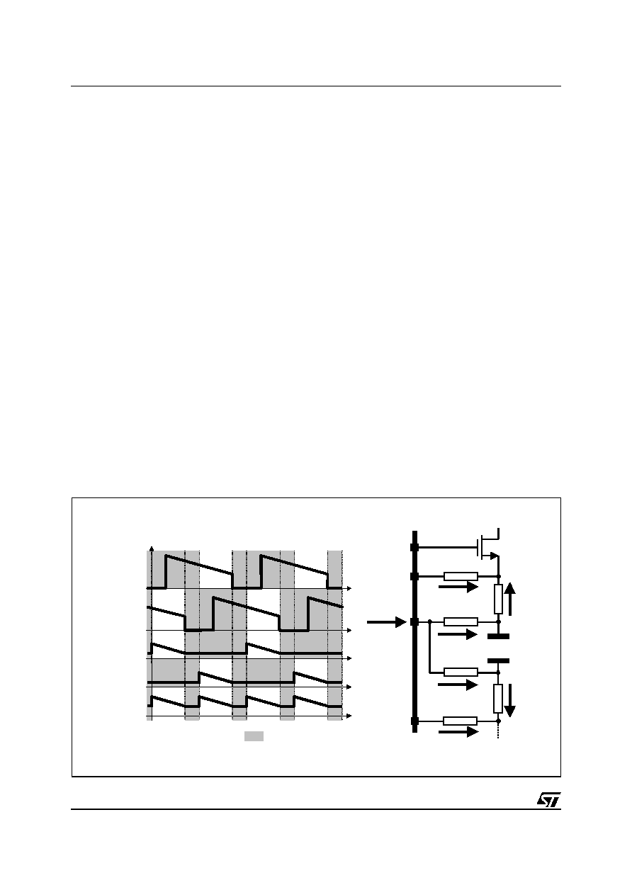
of the OFF time reducing noise injection into the device due to the mosfet turn-on (See fig. 3). Track time
must be at least 200ns to make proper reading of the delivered current.
This circuit sources a constant 100
µA current from the PGNDS pin: it must be connected through two
equal Rg resistors to the groundside of the sensing element (See Figure 3). The two current reading cir-
cuitry uses this pin as a reference keeping the ISENx pin to this voltage.
The current that flows in the ISENx pin is then given by the following equation:
Where R
SENSE
is an external sense resistor or the R
dsON
of the low side mosfet and Rg is the transcon-
ductance resistor used between ISENx and PGNDS pins toward the reading points; I
PHASEx
is the current
carried by the relative phase. The current information reproduced internally is represented by the second
term of the previous equation as follow:
CH3 = HGATE1; CH4 = HGATE2
CH3 = LGATE1; CH4 = LGATE2
I
ISEN x
50
µA
R
SEN SE
I
PH AS Ex
R
g
------------------------------------------------
50
µA I
IN FO x
+
=
+
=
I
IN FO x
R
SEN SE
I
PH AS Ex
R
g
------------------------------------------------
=
L6710
12/34
Since the current is read in differential mode, also negative current information is kept; this allow the de-
vice to check for dangerous returning current between the two phases assuring the complete equalization
between the phase's currents. From the current information of each phase, information about the total cur-
rent delivered (I
FB
=I
INFO1
+ I
INFO2
) and the average current for each phase (I
AVG
= (I
INFO1
+ I
INFO2
)/2 )
is taken. I
INFOX
is then compared to I
AVG
to give the correction to the PWM output in order to equalize the
current carried by the two phases.
The transconductance resistor Rg can be designed in order to have current information of 25
µA per phase
at full nominal load; the over current intervention threshold is set at 140% of the nominal (I
INFOx
= 35
µA).
According to the above relationship, the over current threshold (I
OCPx
) for each phase, which has to be
placed at 1/2 of the total delivered maximum current, results:
Since the device senses the output current across the low-side mosfets (or across a sense resistors in
series with them) the device limits the bottom of the inductor current triangular waveform: an over current
is detected when the current flowing into the sense element is greater than I
OCPx
(I
INFOx
>35
µA).
Introducing now the maximum ON time dependence with the delivered current (where T is the switching
period T=1/F
SW
):
Where I
OUT
is the output current.
This linear dependence has a value at zero load of 0.80∑T and at maximum current of 0.40∑T typical and
results in two different behaviors of the device:
Figure 3. Current reading timing (left) and circuit (right)
I
OC Px
35
µA Rg
R
SEN S E
--------------------------- Rg
I
OC Px
R
SEN SE
35
µA
------------------------------------------
=
=
T
O N ,MAX
0.80
I
FB
≠
5.73k
(
) T
0.80
R
SEN S E
Rg
---------------------- I
O U T
5.73k
≠
T =
T
0.80 T I
FB
0
µA
=
=
T
0.40 T I
FB
70
µA
=
=
=
=
R
SE
N
S
E
Rg
50
µA
I
ISEN1
I
PH
A
SE1
Rg
LGATE1
ISEN1
PGNDS
Rg
50
µA
100
µA
I
P
H
A
SE2
Rg
ISEN2
R
SEN
SE
I
ISEN2
TOTAL
CURRENT
INFO (I
FB
)
I
LS1
I
LS2
Track & Hold
I
INFO2
I
INFO1

13/34
L6710
1.
T
ON
LIMITED OUTPUT VOLTAGE.
This happens when the maximum ON time is reached before the current in each phase reaches I
OCPx
(I
INFOx
<35 A).
Figure 4a shows the maximum output voltage that the device is able to regulate considering the T
ON
lim-
itation imposed by the previous relationship. If the desired output characteristic crosses the T
ON
limited
maximum output voltage, the output resulting voltage will start to drop after crossing. In this case, the de-
vice doesn't perform constant current limitation but only limits the maximum ON time following the previous
relationship. The output voltage follows the resulting characteristic (dotted in Figure 4b) until UVP is de-
tected or anyway until I
FB
= 70
µA
Figure 4. T
ON
Limited Operation
2.
CONSTANT CURRENT OPERATION
This happens when ON time limitation is reached after the current in each phase reaches I
OCPx
(I
INFOx
>35
µA).
The device enters in Quasi-Constant-Current operation: the low-side mosfets stays ON until the current
read becomes lower than I
OCPx
(I
INFOx
< 35
µA) skipping clock cycles. The high side mosfets can be turned
ON with a T
ON
imposed by the control loop at the next available clock cycle and the device works in the
usual way until another OCP event is detected.
This means that the average current delivered can slightly increase also in Over Current condition since
the current ripple increases. In fact, the ON time increases due to the OFF time rise because of the current
has to reach the I
OCPx
bottom. The worst-case condition is when the ON time reaches its maximum value.
When this happens, the device works in Constant Current and the output voltage decrease as the load
increase. Crossing the UVP threshold causes the device to latch (FAULT pin is driven high).
Figure 5 shows this working condition.
It can be observed that the peak current (Ipeak) is greater than the IOCPx but it can be determined as
follow:
Where V
outMIN
is the minimum output voltage (VID-40% as follow).
The device works in Constant-Current, and the output voltage decreases as the load increase, until the
0.80∑V
IN
0.40∑V
IN
V
OUT
I
OUT
I
OCP
=2∑I
OCPx
(I
FB
=70
µA)
T
ON
Limited Output
characteristic
0.80∑V
IN
0.40∑V
IN
V
OUT
I
OUT
I
OCP
=2∑I
OCPx
(I
FB
=70
µA)
Desired Output
characteristic and
UVP threshold
Resulting Output
characteristic
a) Maximum output Voltage
b) T
ON
Limited Output Voltage
I
pea k
I
O C Px
V
IN
V out
mi n
≠
L
------------------------------------- Ton
M AX
I
O C Px
V
I N
Vou t
M IN
≠
L
-------------------------------------- 0.40 T
+
=
+
=

L6710
14/34
output voltage reaches the under-voltage threshold (V
outMIN
). When this threshold is crossed, all mosfets
are turned off, the FAULT pin is driven high and the device stops working. Cycle the power supply to re-
start operation.
The maximum average current during the Constant-Current behavior results:
In this particular situation, the switching frequency results reduced. The ON time is the maximum allowed
(TonMAX) while the OFF time depends on the application:
Over current is set anyway when I
INFOx
reaches 35
µA (I
FB
=70
µA).
The full load value is only a convention to work with convenient values for I
FB
. Since the OCP intervention
threshold is fixed, to modify the percentage with respect to the load value, it can be simply considered that,
for example, to have on OCP threshold of 200%, this will correspond to I
INFOx
= 35
µA (I
FB
= 70
µA). The
full load current will then correspond to I
INFOx
= 17.5
µA (I
FB
= 35
µA).
Figure 5. Constant Current operation
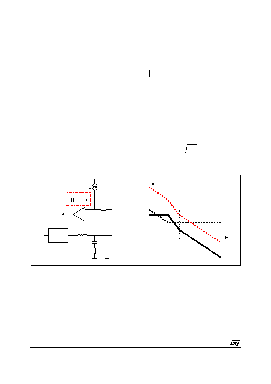
INTEGRATED DROOP FUNCTION
The device uses a droop function to satisfy the requirements of high performance microprocessors, re-
ducing the size and the cost of the output capacitor.
This method "recovers" part of the drop due to the output capacitor ESR in the load transient, introducing
a dependence of the output voltage on the load current: the regulated voltage decrease as the load in-
crease with a precise relationship.
As shown in figure 6, the ESR drop is present in any case, but using the droop function the total deviation
of the output voltage is minimized. A static error (V
DROOP
in figure 6) at zero load is simply introduced by
a resistor between FB and GND allowing to exploit the all tolerance interval available. This additional re-
sistor is not required in application such as VRD10 since the nominal value is already set by the VID* and
the load regulation fixed by the specs.
Since the device has an average current mode regulation, the information about the total current delivered
I
MA X,TOT
2 I
MA X
2
I
O C Px
I peak
I
O C Px
≠
2
--------------------------------------
+
=
=
T
O FF
L
I peak
I
O C Px
≠
V
OU t
-------------------------------------- f
1
T
O N m ax
T
O FF
+
-----------------------------------------
=
=
TonMAX
TonMAX
I
OCPx
Ipeak
I
MAX
Vout
Iout
(I
FB
=50
µA)
2∑I
OCPx
(I
FB
=70
µA)
I
MAX,TOT
UVP
Droop effect
a) Maximum current for each phase
b) Output Characteristic

15/34
L6710
is used to implement the Droop Function. This current I
FB
(equal to the sum of both I
I
NFOx
) is sourced from
the FB pin. Connecting a resistor between this pin and Vout, the total current information flows only in this
resistor because the compensation network between FB and COMP has always a capacitor in series (See
fig. 7). The voltage regulated is then equal to:
Since I
FB
depends on the current information about the two phases, the output characteristic vs. load cur-
rent is given by:
Where I
LOAD
is the output current of the system and R
DROOP
is its equivalent output resistance.
The feedback current is equal to 50
µA at nominal full load (I
FB
= I
INFO1
+ I
INFO2
) and 70
µA at the OC in-
tervention threshold, so the maximum output voltage deviation is equal to:
Figure 6. Output transient response without (a) and with (b) the droop function
Figure 7. Active Droop Function Circuit
REMOTE VOLTAGE SENSE
A remote sense buffer is integrated into the device to allow output voltage remote sense implementation
without any additional external components. In this way, the output voltage programmed is regulated be-
tween the remote buffer inputs compensating motherboard trace losses or connector losses if the device
V
OUT
VI D* R
FB
I
FB
≠
=
V
OUT
VI D* R
DROOP
I
LO AD
VID* R
F B
R
SE NSE
Rg
---------------------- I
L O AD
≠
=
≠
=
V
FUL L
P O SITIVE
≠
LO AD
≠
R
FB
50
µA V
O C
INTERV ENTIO N
≠
R
FB
70
µA
≠
=
≠
=
V
MAX
V
MIN
V
NOM
(a)
(b)
ESR DROP
ESR DROP
V
DROOP
Ref
COMP
FB
To V
OUT
Total Current Info (I
INFO1
+I
INFO2
)
V
DROOP
R
FB
Ref
COMP
FB
To V
OUT
Total Current Info (I
INFO1
+I
INFO2
)
V
DROOP
R
FB

L6710
16/34
is used for a VRM module. The very low offset amplifier senses the output voltage remotely through the
pins FBR and FBG (FBR is for the regulated voltage sense while FBG is for the ground sense) and reports
this voltage internally at VSEN pin with unity gain eliminating the errors. Keeping the FBR and FBG traces
parallel and guarded by a power plane results in common mode coupling for any picked-up noise.
If remote sense is not required, it is enough connecting R
FB
directly to the regulated voltage: VSEN be-
comes not connected and still senses the output voltage through the remote buffer. In this case the FBG
and FBR pins must be connected anyway to the regulated voltage (See figure 9).
The remote buffer is included in the trimming chain in order to achieve ±0.5% accuracy on the output volt-
age when the RB Is used: eliminating it from the control loop causes the regulation error to be increased
by the RB offset worsening the device performances.
Figure 8. Remote Buffer Connections
OUTPUT VOLTAGE MONITOR PROTECTION
The device monitors through pin VSEN the regulated voltage in order to build the PGOOD signal and man-
age the OVP / UVP conditions comparing this voltage level with the programmed reference VID*.
Power good output is forced low if the voltage sensed by VSEN is not within ±12% (Typ.) of the pro-
grammed value. It is an open drain output and it is enabled only after the soft start is finished (2048 clock
cycles after start-up). During Soft-Start this pin is forced low.
Under voltage protection is provided. If the output voltage monitored by VSEN drops below the 60% of the
reference voltage for more than one clock period, the device turns off all mosfets and the OSC/FAULT is
driven high (5V). The condition is latched, to recover it is required to cycle the power supply.
Over Voltage protection is also provided:
Once VCC crosses the turn-ON threshold, when the voltage monitored by VSEN reaches 125% (Typ.) of
the programmed voltage the controller permanently switches on both the low-side mosfets and switches
off both the high-side mosfets in order to protect the CPU. The OSC/ FAULT pin is driven high (5V) and
power supply (Vcc) turn off and on is required to restart operations.
Both Over Voltage and Under Voltage are active also during soft start (Under Voltage after than the output
voltage reaches 0.6V). The reference used in this case to determine the UV thresholds is the increasing
voltage driven by the 2048 soft start digital counter while the reference used for the OV threshold is the
final reference programmed by the VID pins.
Reference
I
FB
REMOTE
BUFFER
ERROR
AMPLIFIER
FB
COMP
VSEN
FBG
FBR
Remote
Ground
Remote
V
OUT
R
F
C
F
R
FB
32k
32k
32k
32k
Reference
I
FB
REMOTE
BUFFER
ERROR
AMPLIFIER
FB
COMP
VSEN
FBG
FBR
R
F
C
F
R
FB
32k
32k
32k
32k
V
OUT
RB used (±0.5% Accuracy)
RB Not Used

17/34
L6710
Figure 9. OVP (left) and UVP (right) latch.
SOFT START, INHIBIT AND POWER DOWN
At start-up a ramp is generated increasing the loop reference from 0V to the final value programmed by
VID in 2048 clock periods as shown in figure 10.
Once the soft start begins, the reference is increased: upper and lower MOS begin to switch and the output
voltage starts to increase with closed loop regulation. At the end of the digital soft start, the Power Good
comparator is enabled and the PGOOD signal is then driven high (See fig. 10). The Under Voltage com-
parator is enabled when the reference voltage reaches 0.6V. The Soft-Start will not take place, if both VCC
and VCCDR pins are not above their own turn-on thresholds.
During normal operation, if any under-voltage is detected on one of the two supplies the device shuts
down. Forcing the OUTEN pin to a voltage lower than 0.4V (Typ.) disables the device: all the power mos-
fets and protections are turned off until the condition is removed.
Figure 10. Soft Start
LGATEx
OSC/FAULT
OUTEN
REF_OUT
LGATEx
OSC/FAULT
OUTEN
REF_OUT
V
CC
=V
CCDR
V
LGATEx
PGOOD
V
OUT
t
t
t
t
Turn ON threshold
2048 Clock Cycles
Timing Diagram
Acquisition:
CH1=PGOOD; CH2=REF_OUT;
CH3=VOUT; CH4=LGATEx)

L6710
18/34
Figure 11. Power Down: 0A (left), resistive load (right); CH1= Vout; CH2,CH3 = LS; CH4 =V in
When shutting the system down, the device continues regulating until Vcc becomes lower than the turn-
off threshold. After that point, the device will shut down all power mosfets.
INPUT CAPACITOR
The input capacitor is designed considering mainly the input RMS current that depends on the duty cycle
as reported in figure 12. Considering the dual-phase topology, the input RMS current is highly reduced
comparing with a single-phase operation. It can be observed that the input RMS value is one half of the
single-phase equivalent input current in the worst case condition that happens for D=0.25 and D=0.75.
The power dissipated by the input capacitance is then equal to:
Input capacitor is designed in order to sustain the ripple relative to the maximum load duty cycle. To reach
the high RMS value needed by the CPU power supply application and also to minimize components cost,
the input capacitance is realized by more than one physical capacitor. The equivalent RMS current is sim-
ply the sum of the single capacitor's RMS current.
Figure 12. Input RMS Current vs. Duty Cycle (D) and Driving Relationships.
P
RM S
ESR
I
RM S
(
)
2
=
0.50 0.75
0.25
0.50
0.25
Single Phase
Dual Phase
Duty Cycle (V
OUT
/V
IN
)
R
m
s
C
u
rr
ent
N
o
rm
a
l
i
z
ed (I
RM
S
/I
OU
T
)
I
rm s
I
OUT
2
------------
2D
1
2D
≠
(
)
if D < 0.5
I
OUT
2
------------
2 D
1
≠
(
) 2 2D
≠
(
)
if D > 0.5
=
Where D = V
OUT
/V
IN
is the operative duty cycle for each phase

19/34
L6710
Input bulk capacitor must be equally divided between high-side drain mosfets and placed as close as pos-
sible to reduce switching noise above all during load transient. Ceramic capacitor can also introduce ben-
efits in high frequency noise decoupling, noise generated by parasitic components along power path.
OUTPUT CAPACITOR
Since the microprocessors require a current variation beyond 50A doing load transients, with a slope in
the range of tenth A/
µs, the output capacitor is a basic component for the fast response of the power sup-
ply.
Dual phase topology reduces the amount of output capacitance needed because of faster load transient
response (switching frequency is doubled at the load connections). Current ripple cancellation due to the
180∞ phase shift between the two phases also reduces requirements on the output ESR to sustain a spec-
ified voltage ripple.
When a load transient is applied to the converter's output, for first few microseconds the current to the load
is supplied by the output capacitors. The controller recognizes immediately the load transient and increas-
es the duty cycle, but the current slope is limited by the inductor value.
The output voltage has a first drop due to the current variation inside the capacitor (neglecting the effect
of the ESL):
A minimum capacitor value is required to sustain the current during the load transient without discharge
it. The voltage drop due to the output capacitor discharge is given by the following equation:
Where D
MAX
is the maximum duty cycle value. The lower is the ESR, the lower is the output drop during
load transient and the lower is the output voltage static ripple.
INDUCTOR DESIGN
The inductance value is defined by a compromise between the transient response time, the efficiency, the
cost and the size. The inductor has to be calculated to sustain the output and the input voltage variation
to maintain the ripple current
I
L
between 20% and 30% of the maximum output current. The inductance
value can be calculated with this relationship:
Where F
SW
is the switching frequency, V
IN
is the input voltage and V
OUT
is the output voltage.
Increasing the value of the inductance reduces the ripple current but, at the same time, reduces the con-
verter response time to a load transient. The response time is the time required by the inductor to change
its current from initial to final value. Since the inductor has not finished its charging time, the output current
is supplied by the output capacitors. Minimizing the response time can minimize the output capacitance
required.
The response time to a load transient is different for the application or the removal of the load: if during
the application of the load the inductor is charged by a voltage equal to the difference between the input
and the output voltage, during the removal it is discharged only by the output voltage. The following ex-
pressions give approximate response time for I load transient in case of enough fast compensation net-
work response:
V
OUT
I
OUT
ESR
=
V
OUT
I
2
OUT
L
4 C
OUT
V
In
d
m a x
V
OUT
≠
(
)
-------------------------------------------------------------------------------
=
L
V
IN
V
OUT
≠
fs
I
L
------------------------------
V
OUT
V
IN
--------------
=

L6710
20/34
The worst condition depends on the input voltage available and the output voltage selected. Anyway the
worst case is the response time after removal of the load with the minimum output voltage programmed
and the maximum input voltage available.
MAIN CONTROL LOOP
The control loop is composed by the Current Sharing control loop and the Average Current Mode control
loop. Each loop gives, with a proper gain, the correction to the PWM in order to minimize the error in its
regulation: the Current Sharing control loop equalize the currents in the inductors while the Average Cur-
rent Mode control loop fixes the output voltage equal to the reference programmed by VID. Figure 13 re-
ports the block diagram of the main control loop.
Figure 13. Main Control Loop Diagram
Current Sharing (CS) Control Loop
Active current sharing is implemented using the information from Tran conductance differential amplifier
in an average current mode control scheme.
A current reference equal to the average of the read current (I
AVG
) is internally built; the error between the
read current and this reference is converted to a voltage with a proper gain and it is used to adjust the duty
cycle whose dominant value is set by the error amplifier at COMP pin (See fig. 14).
The current sharing control is a high bandwidth control loop allowing current sharing even during load tran-
sients.
The current sharing error is affected by the choice of external components; choose precise Rg resistor
(±1% is necessary) to sense the current.
The current sharing error is internally dominated by the voltage offset of Tran conductance differential am-
plifier; considering a voltage offset equal to 2mV across the sense resistor, the current reading error is
given by the following equation
t
app lic atio n
L
I
V
IN
V
OUT
≠
------------------------------ t
re m ov al
L
I
V
OUT
--------------
=
=
L1
L2
+
+
PWM1
1/5
+
-
1/5
I
INFO2
I
INFO1
4/5
Z
F(S)
PWM2
C
O
FB
COMP
R
O
ERROR
AMPLIFIER
REFERENCE
PROGRAMMED
BY VID
CURRENT
SHARING
DUTY CYCLE
CORRECTION
R
FB
D02IN1392
I
REA D
I
M AX
--------------------
2mV
R
SENSE
I
M AX
---------------------------------------
=

21/34
L6710
Figure 14. Current Sharing Control Loop.
Where
I
READ
is the difference between one phase current and the ideal current (I
MAX
/2).
For Rsense=4m
and Imax=40A the current sharing error is equal to 2.5%, neglecting errors due to Rg
and Rsense mismatches.
Average Current Mode (ACM) Control Loop
The average current mode control loop is reported in figure 15. The current information IFB sourced by
the FB pin flows into RFB implementing the dependence of the output voltage from the read current.
The ACM control loop gain results (obtained opening the loop after the COMP pin)
Where:
is the equivalent output resistance determined by the droop function;
Z
P
(s) is the impedance resulting by the parallel of the output capacitor (and its ESR) and the applied
load Ro;
Z
F
(s) is the compensation network impedance;
Z
L
(s) is the parallel of the two inductor impedance;
A(s) is the error amplifier gain;
is the ACM PWM transfer function where Vosc is the oscillator ramp amplitude and
has a typical value of 3V
Removing the dependence from the Error Amplifier gain, so assuming this gain high enough, the control
loop gain results:
With further simplifications, it results:
L1
L2
+
+
PWM1
1/5
1/5
I
INFO2
I
INFO1
PWM2
COMP
V
OUT
CURRENT
SHARING
DUTY CYCLE
CORRECTION
D02IN1393
G
LO O P
s
)
( )
PWM Z
F
s
( ) R
DROOP
Z
P
s
( )
+
(
)
Z
P
s
( ) Z
L
s
( )
+
(
)
Z
F
s
( )
A s
( )
---------------
1
1
A s
( )
------------
+
R
FB
+
--------------------------------------------------------------------------------------------------------------------
≠
=
R
DROOP
Rsense
Rg
---------------------- R
FB
=
PWM
4
5
---
V
IN
V
O SC
-------------------
=
G
LO O P
s
( )
4
5
---
V
IN
V
O SC
-------------------
Z
F
s
( )
Z
P
s
( ) Z
L
s
( )
+
------------------------------------
Rs
Rg
--------
Z
P
s
( )
R
F B
---------------
+
≠
=
G
LO O P
s
( )
4
5
---
V
IN
V
O SC
-------------------
Z
F
s
( )
R
FB
---------------
Ro
R
DROOP
+
Ro
R
L
2
-------
+
-------------------------------------
1
s Co
R
DROOP
//Ro
ESR
+
(
)
+
s
2
Co
L
2
---
s
L
2 Ro
---------------
Co E SR
Co
R
L
2
-------
+
+
1
+
+
----------------------------------------------------------------------------------------------------------------------------------
≠
=
L6710
22/34
Considering now that in the application of interest it can be assumed that Ro>>R
L
; ESR<<Ro and
R
DROOP
<<Ro, it results:
The ACM control loop gain is designed to obtain a high DC gain to minimize static error and cross the 0dB
axes with a constant -20dB/dec slope with the desired crossover frequency
T
. Neglecting the effect of
Z
F
(s), the transfer function has one zero and two poles. Both the poles are fixed once the output filter is
designed and the zero is fixed by ESR and the Droop resistance. To obtain the desired shape an R
F
-C
F
series network is considered for the Z
F
(s) implementation. A zero at
F
=1/R
F
C
F
is then introduced togeth-
er with an integrator. This integrator minimizes the static error while placing the zero in correspondence
with the L-C resonance a simple -20dB/dec shape of the gain is assured (See Figure 15). In fact, consid-
ering the usual value for the output filter, the LC resonance results to be at frequency lower than the above
reported zero.
Compensation network can be simply designed placing
Z
=
LC
and imposing the cross-over frequency
T as desired obtaining:
Figure 15. ACM Control Loop Gain Block Diagram (left) and Bode Diagram (right).
LAYOUT GUIDELINES
Since the device manages control functions and high-current drivers, layout is one of the most important
things to consider when designing such high current applications.
A good layout solution can generate a benefit in lowering power dissipation on the power paths, reducing
radiation and a proper connection between signal and power ground can optimize the performance of the
control loops.
Integrated power drivers reduce components count and interconnections between control functions and
drivers, reducing the board space.
Here below are listed the main points to focus on when starting a new layout and rules are suggested for
a correct implementation.
G
LO O P
s
( )
4
5
---
V
IN
V
O SC
-------------------
Z
F
s
( )
R
F B
---------------
1
s Co
R
DROOP
ESR
+
(
)
+
s
2
Co
L
2
---
s
L
2 Ro
---------------
Co ESR
Co
R
L
2
-------
+
+
1
+
+
----------------------------------------------------------------------------------------------------------------------------------
≠
=
R
F
R
F B
V
O SC
V
IN
----------------------------------
5
4
---
T
L
2
R
DROOP
ESR
+
(
)
------------------------------------------------------- C
F
Co
L
2
---
R
F
--------------------
=
=
Rout
Cout
ESR
L/2
R
FB
R
F
C
F
REF
PWM
I
FB
V
COMP
V
OUT
d
∑V
IN
Z
F
dB
T
Z
LC
G
LOOP
Z
F
(s)
K
dB
FB
OSC
IN
R
1
V
V
5
4
K
=

23/34
L6710
Figure 16. Power connections and related connections layout guidelines (same for both phases).
≠ Power Connections.
These are the connections where switching and continuous current flows from the input supply towards
the load. The first priority when placing components has to be reserved to this power section, minimizing
the length of each connection and loop as much as possible. To minimize noise and voltage spikes (EMI
and losses) these interconnections must be a part of a power plane and anyway realized by wide and thick
copper traces: loop must be anyway minimized. The critical components, i.e. the power transistors, must
be located as close as possible one to the other.
Fig. 16a shows the details of the power connections involved and the current loops. The input capacitance
(C
IN
), or at least a portion of the total capacitance needed, has to be placed close to the power section in
order to eliminate the stray inductance generated by the copper traces. Low ESR and ESL capacitors are
required.
Use as much VIAs as possible when power traces have to move between different planes on the PCB:
this reduces both parasitic resistance and inductance. Moreover, reproducing the same high-current trace
on more than one PCB layer will reduce the parasitic resistance associated to that connection.
Connect output bulk capacitor as near as possible to the load, minimizing parasitic inductance and resis-
tance associated to the copper trace also adding extra decoupling capacitors along the way to the load
when this results in being far from the bulk capacitor bank.
≠ Power Connections Related.
Fig.16b shows some small signal components placement, and how and where to mix signal and power
ground planes. The distance from drivers and mosfet gates should be reduced as much as possible. Prop-
agation delay times as well as for the voltage spikes generated by the distributed inductance along the
copper traces are so minimized.
In fact, the further the mosfet is from the device, the longer is the interconnecting gate trace and as a con-
sequence, the higher are the voltage spikes corresponding to the gate PWM rising and falling signals.
Even if these spikes are clamped by inherent internal diodes, propagation delays, noise and potential
causes of instabilities are introduced jeopardizing good system behavior. One important consequence is
that the switching losses for the high side mosfet are significantly increased.
For this reason, it is suggested to have the device oriented with the driver side towards the mosfets and
the GATEx and PHASEx traces walking together toward the high side mosfet in order to minimize distance
(see fig 17). In addition, since the PHASEx pin is the return path for the high side driver, this pin must be
connected directly to the High Side mosfet Source pin to have a proper driving for this mosfet.
For the LS mosfets, the return path is the PGND pin: it can be connected directly to the power ground
plane (if implemented) or in the same way to the LS mosfets Source pin. GATEx and PHASEx connections
(and also PGND when no power ground plane is implemented) must also be designed to handle current
peaks in excess of 2A (30 mils wide is suggested).
V
IN
LOAD
HS
R
gate
LS
R
gate
HGATEx
PHASEx
LGATEx
PGNDx
C
IN
C
OUT
L
D
C
BOOTx
V
IN
LOAD
HS
LS
BOOTx
PHASEx
VCC
SGND
C
IN
C
OUT
L
D
+V
CC
C
VCC
a. PCB power and ground planes areas
b. PCB small signal components placement

L6710
24/34
Figure 17. Device orientation (left) and sense nets routing (right).
Gate resistors of few ohms help in reducing the power dissipated by the IC without compromising the sys-
tem efficiency.
The placement of other components is also important:
∑ The bootstrap capacitor must be placed as close as possible to the BOOTx and PHASEx pins to mini-
mize the loop that is created.
∑ Decoupling capacitor from VCC AND SGND placed as close as possible to the involved pins.
∑ Decoupling capacitor from VCCDR and PGND placed as close as possible to those pins. This capacitor
sustains the peak currents requested by the low-side mosfet drivers.
∑ Refer to SGND all the sensible components such as frequency set-up resistor (when present) and also
the optional resistor from FB to GND used to give the positive droop effect.
∑ Connect SGND to PGND on the load side (output capacitor) to avoid undesirable load regulation effect
and to ensure the right precision to the regulation when the remote sense buffer is not used. Connect
anyway in a single point (star grounding).
∑ An additional 100nF ceramic capacitor is suggested to place near HS mosfet drain. This helps in reduc-
ing noise.
∑ Filtering VSEN pin vs. GND with 1nF capacitor helps in reducing noise injection into device.
∑ Filtering OUTEN pin vs. GND helps in reducing false trip due to coupled noise: take care in routing driv-
ing net for this pin in order to minimize coupled noise.
∑ PHASE pin spikes. Since the HS mosfet switches in hard mode, heavy voltage spikes can be observed
on the PHASE pins. If these voltage spikes overcome the max breakdown voltage of the pin, the device
can absorb energy and it can cause damages. The voltage spikes must be limited by proper layout, the
use of gate resistors, Schottky diodes in parallel to the low side mosfets and/or snubber network on the
low side mosfets, to a value lower than 26V, for 20nSec, at F
SW
of 600kHz max.
≠ Current Sense Connections.
∑ Remote Buffer: The input connections for this component must be routed as parallel nets from the
FBG/FBR pins to the load in order to compensate losses along the output power traces and also to
avoid the pick-up of any common mode noise. Connecting these pins in points far from the load will
cause a non-optimum load regulation, increasing output tolerance.
∑ Current Reading: The Rg resistors have to be placed as close as possible to the ISENx and PGNDS
pins in order to limit the noise injection into the device. Moreover, PGNDS trace must be divided just
To HS Mosfet
(30 mils wide)
To HS Mosfet
(30 mils wide)
To LS Mosfets
(30 mils wide)
T
o
LS
M
o
s
f
et
(
o
r
Se
n
s
e
R
e
si
st
o
r
)
To
L
S
M
o
s
f
e
t
(o
r Se
n
s
e
R
e
si
st
o
r
)
T
o
r
egul
at
e
d
Ou
t
p
ut
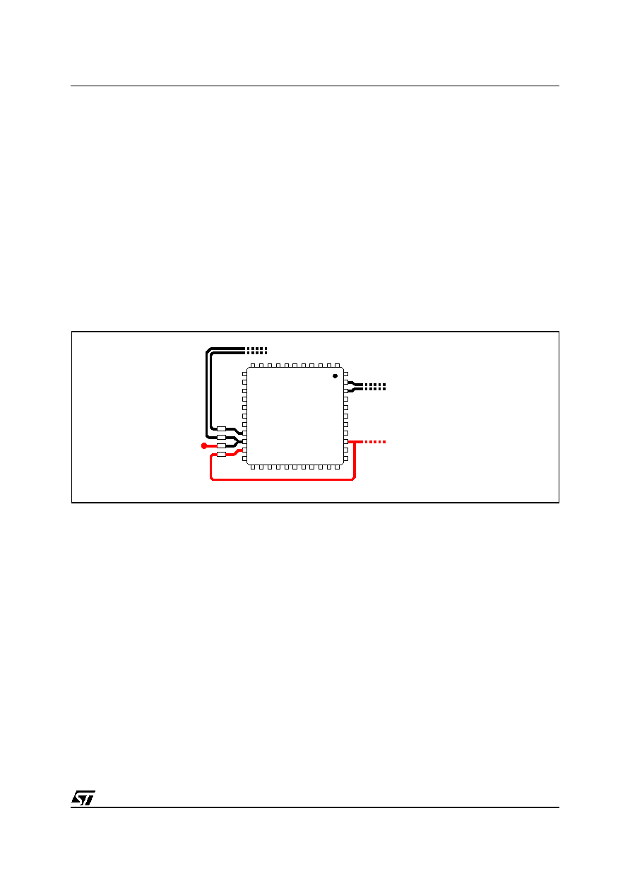
25/34
L6710
after the pin and connected through Rg to the sense point (see Fig. 17). The PCB traces connecting
these resistors to the reading point must be routed as parallel traces in order to avoid the pick-up of any
common mode noise. It's also important to avoid any offset in the measurement and to get a better pre-
cision, to connect the traces as close as possible to the sensing elements, dedicated current sense re-
sistor or low side mosfet R
dsON
.
Moreover, when using the low side mosfet R
dsON
as current sense element, the ISENx pin is practically
connected to the PHASEx pin. DO NOT CONNECT THE PINS TOGETHER AND THEN TO THE HS
SOURCE! The device won't work properly because of the noise generated by the return of the high side
driver. In this case route two separate nets: connect the PHASEx pin to the HS Source (route together
with HGATEx) with a wide net (30 mils) and the ISENx pin to the LS Drain (route together with PGNDS).
Moreover, the PGNDS pin is always connected, through the Rg resistor, to the PGND: DO NOT CON-
NECT DIRECTLY TO THE PGND! In this case the device won't work properly. Route anyway to the LS
mosfet source (together with ISENx net).
Right and wrong connections are reported in Figure 18.
Symmetrical layout is also suggested to avoid any unbalance between the two phases of the converter.
Figure 18. PCB layout connections for sense nets.
EMBEDDING L6710-BASED VRMs...
When embedding the VRM into the application, additional care must be taken since the whole VRM is a
switching DC/DC regulator and the most common system in which it has to work is a digital system such
as MB or similar. In fact, latest MB has become faster and powerful: high speed data bus are more and
more common and switching-induced noise produced by the VRM can affect data integrity if not following
additional layout guidelines. Few easy points must be considered mainly when routing traces in which
switching high currents flow (switching high currents cause voltage spikes across the stray inductance of
the traces causing noise that can affect the near traces):
≠ When reproducing high current path on internal layers, please keep all layers the same size in order
to avoid "surrounding" effects that increases noise coupling.
≠ Keep safe guarding distance between high current switching VRM traces and data buses, especially
if high-speed data bus to minimize noise coupling.
≠ Keep safe guard distance or filter properly when routing bias traces for I/O sub-systems that must
walk near the VRD.
≠ Possible causes of noise can be located in the PHASE connections, Mosfet gate drive and Input volt-
age path (from input bulk capacitors and HS drain). Also PGND connections must be considered if
not insisting on a power ground plane. These connections, that can be possible sources of noise,
must be carefully kept far away from noise-sensitive data bus.
To LS Drain and Source
(or Sense Resistor)
To HS Gate and Source
(30 mils wide)
To HS Source
VIA to
GND Plane
NOT CORRECT
CORRECT

L6710
26/34
Since the generated noise is mainly due to the switching activity of the VRM, noise emissions depend on
how fast the current switch. To reduce noise emission levels, it is also possible, in addition to the previous
guidelines, to reduce the current slope and then to increase the switching times: this will cause, as a con-
sequence of the higher switching time, an increase in switching losses that must be considered in the ther-
mal design of the system.
Figure 19. - Layout Suggestions (not in scale).
Application Board Description
The application board shows the operation of the device in a dual phase application. This evaluation board
allows output voltage adjustability (0.8375V - 1.6000V) through the switches S0-S4 and high output cur-
rent capability.
The board has been laid out with the possibility to use up to two D
2
PACK mosfets for the low side switch
in order to give maximum flexibility in the mosfet choice.
The four layers demo board's copper thickness is of 70
µm in order to minimize conduction losses consid-
ering the high current that the circuit is able to deliver.
Demo board schematic circuit is reported in Figure 20.
Several jumpers allow setting different configurations for the device: JP3, JP4 and JP5 allow configuring
the remote buffer as desired. Simply shorting JP4 and JP5 the remote buffer is enabled and it senses the
output voltage on-board; to implement a real remote sense, leave these jumpers open and connect the
FBG and FBR connectors on the demo board to the remote load.
To avoid using the remote buffer, simply short all the jumpers JP3, JP4 and JP5. Local sense through the
R7 is used for the regulation.
The input can be configured in different ways using the jumpers JP1, JP2 and JP6; these jumpers control
also the mosfet driver supply voltage. Anyway, power conversion starts from VIN and the device is sup-
plied from V
CC
(See Figure 21).
ATX 12 CONNECTOR
INPUT POWER PLANE
PHASE PLANE
PHASE PLANE
OUTPUT
POWER PLANE
OUTPUT BULK
CAPACITORS
INPUT CAPS
CERAMIC
DECOUPLING
CAPACITORS
NTC FOR
THERMAL
COMPENSATION
SAFELY FAR
HIGH SPEED
DATA BUS

27/34
L6710
Figure 20. Demo Board Schematic
Figure 21. Power supply configuration
Two main configurations can be distinguished: Single Supply (V
CC
=V
IN
=12V) and Double Supply
(V
CC
=12V V
IN
=5V or different).
≠ Single Supply: In this case JP6 has to be completely shorted. The device is supplied with the same
rail that is used for the conversion. With an additional zener diode DZ1 a lower voltage can be derived
to supply the mosfets driver if Logic level mosfet are used. In this case JP1 must be left open so that
the HS driver is supplied with V
IN
-V
DZ1
through BOOTx and JP2 must be shorted to the left to use
VIN or to the right to use V
IN
-V
DZ1
to supply the LS driver through VCCDR pin. Otherwise, JP1 must
be shorted and JP2 can be freely shorted in one of the two positions.
≠ Double Supply: In this case VCC supply directly the controller (12V) while VIN supplies the HS drains
for the power conversion. This last one can start indifferently from the 5V bus (Typ.) or from other
buses allowing maximum flexibility in the power conversion. Supply for the mosfet driver can be pro-
grammed through the jumpers JP1, JP2 and JP6 as previously illustrated. JP6 selects now VCC or
V
IN
depending on the requirements.
Some examples are reported in the following Figures 22 and 23.
L6710
U1
PGOOD
PGND
PGNDS
ISEN2
LGATE2
VSEN
FB
PHASE2
UGATE2
BOOT2
VCC
COMP
SGND
OSC
VID0
VID1
VID2
VID3
VID4
ISEN1
LGATE1
PHASE1
UGATE1
BOOT1
VCCDR
5
31
35
36
38
21
20
41
3
43
42
40
19
28
27
26
24
25
6, 7
39
30
13
9
8
17
18
FBR
FBG
22
C1
R8
C2
R4
R3
Q3
Q4
C3
L2
C7
R11
D3
C6
C11..C14
C15,
C24
R1
JP3
R2
S1
S0
S3
S2
S4
R5
R6
Q1
L1
Q2
C4
D4
C5
Vin
GNDin
GNDCORE
VoutCORE
PGOOD
FBG
FBR
DZ1
C8
JP2
JP1
R13
R15
R12
R14
C9,C10
R9
R18
D1
R17
R16
Q1a
Q3a
D2
R19
R20
JP5
JP4
Vcc
GNDcc
JP6
To
Vcc pin
R21
VID5
29
S5
14
REF_OUT
12
OUTEN
To
PGNDS
C25
R10
L6710 EVALUATION BOARD REV.1
NTC1
R22
To
Vcc pin
C26
OUTEN
R7a
R7
JP7
JP8
C28
Vin
GNDin
DZ1
JP2
JP1
Vcc
GNDcc
JP6
To Vcc pin
To HS Drains (Power Input)
To BOOTx (HS Driver Supply)
To VCCDR pin (LS Driver Supply)
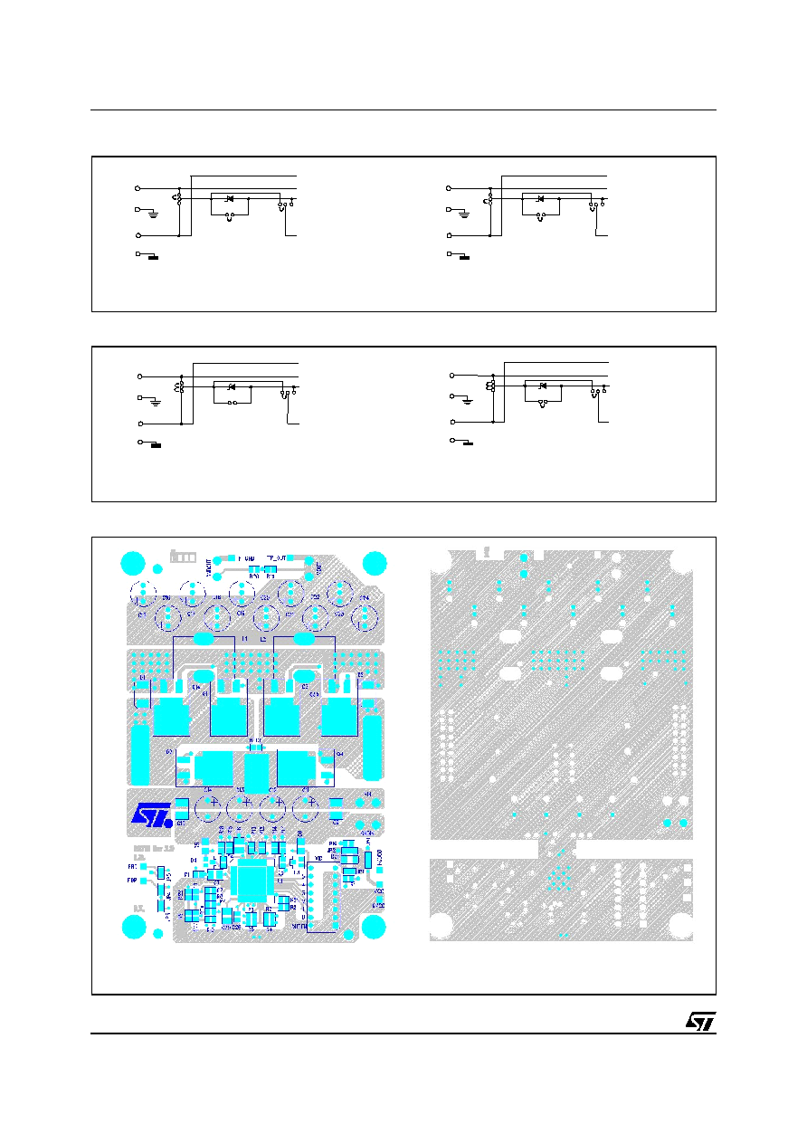
L6710
28/34
Figure 22. Jumpers configuration: Double Supply
Figure 23. Jumpers configuration: Single Supply
Figure 24. PCB and Components Layouts
Vin = 5V
GNDin
DZ1
JP2
JP1
Vcc = 12V
GNDcc
JP6
Vcc = 12V
HS Drains = 5V
HS Supply = 5V
VCCDR (LS Supply) = 5V
Vin = 5V
GNDin
DZ1
JP2
JP1
Vcc = 12V
GNDcc
JP6
Vcc = 12V
HS Drains = 5V
HS Supply = 12V
VCCDR (LS Supply) = 12V
(a) V
CC
=12V; V
BOOTx
=V
CCDR
=V
IN
=5V (b)
V
CC
=V
BOOTx
=V
CCDR
=12V;V
IN
=5V
(a) V
CC
=V
IN
=V
CCDR
=12V; V
BOOTx
=5.2V (b)
V
CC
=V
IN
=V
BOOTx
=V
CCDR
=12V
Vin = 12V
GNDin
DZ1 6.8V
JP2
JP1
Vcc = Open
GNDcc
JP6
Vcc = 12V
HS Drains = 12V
HS Supply = 5.2V
VCCDR (LS Supply) = 12V
Vin = 12V
GNDin
DZ1
JP2
JP1
Vcc = Open
GNDcc
JP6
Vcc = 12V
HS Drains = 12V
HS Supply = 12V
VCCDR (LS Supply) = 12V
Component Side
Internal PGND Plane

29/34
L6710
Figure 25. PCB and Components Layouts
Part List
- 12V
IN
- 1.35V
OUT
- 78A
OUT
(VRD 10)
Code
Value
Description
Vendor
size
Resistors
R1
10k
PGOOD pull-up
SMD 0805
R2, R21
Not Mounted
Frequency modification
SMD 0805
R3, R4, R5, R6
4.7k - 1%
Rg
SMD 0805
R7
2k - 1%
R
FB
network
SMD 0805
R7a
22k - 1%
R
FB
network
SMD 0805
R8
8.2k
R
F
SMD
0805
R9, R22
Not Mounted
Output Voltage Offset
SMD 0805
R10
510
Comp. Network
SMD 0805
R11
82
VCC Filter
SMD 0805
R12, R13, R14, R15
2.2
Gate Resistors
SMD 0805
R16
0
VCCDR Filter
SMD 0805
R17, R18
0
SMD 0805
R19
0
External divider
SMD 0805
R20
Not Mounted
External divider
SMD 0805
NTC1
1k
Thermal compensation
Panasonic ERTJIVT102H
SMD 0603
Internal SGND Plane
Solder Side

L6710
30/34
Capacitors
C1
220p
Comp Network
SMD 0805
C2
22n
C
F
SMD 0805
C3, C4
100n
Bootstrap capacitors
SMD 0805
C5, C6
1µ
Input ceramic capacitors
SMD 1206
C7
10µ
VCC Filter
SMD 1206
C8
10µ
VCCDR Filter
SMD 1206
C9, C10
22µ - 16V
Input Filter
TDK C4532X7R1C226MT
Panas. ECJ4YB1C226M
SMD 1812
SMD 1210
10µ - 16V
TDK C4532X7R1C106MT
SMD 1812
C11, C12, C13, C14
1800µ - 16V
Input Filter
Rubycon MBZ or
Panas. EEUFJ1C182Y
Radial 10x23
Radial 10x25
C15 to C24
2200µ - 6.3V
Output Filter
Rubycon MBZ or
Panas. EEUFL0J222
Radial 10x20
C25
47n
REF_OUT Filter
SMD 0805
C26
1n
VSEN Filter
SMD 0805
C28
47n
Comp. Network
SMD 0805
Diodes
DZ1
Not mounted
Mnimelf
D1, D2
STPS340U
Synch. Diode
STMicroelectronics
SMB
D3, D4
1N4148
Bootstrap diodes
STMicroelectronics
SOT23
Inductors
L1, L2
0.7 µ / 1m
Main inductor
77121 core 4T 2x1.5 mm
Mosfets
Q1, Q1a, Q3, Q3a
STB90NF03L
LS Mosfet
STMicroelectronics
D2PACK
Q2, Q4
STB90NF03L
HS Mosfet
STMicroelectronics
D2PACK
Devices
U1
L6710
PWM controller
STMicroelectronics
TQFP44
Part List
- 12V
IN
- 1.35V
OUT
- 78A
OUT
(VRD 10) (continued)
Code
Value
Description
Vendor
size

31/34
L6710
STATIC PERFORMANCES
Figure 26. - System Efficiency and Mosfet Temperature (Tamb=27deg, 4CFM, 400kHz effective
switching frequency).
Figure 27. Load Regulation.
40
50
60
70
80
90
0
10
20
30
40
50
60
70
80
Output Current [A]
Ef
f
i
ci
ency [
%
]
20
35
50
65
80
95
110
125
0
10
20
30
40
50
60
70
80
Output Current [A]
M
O
S Tem
p
er
at
ur
e [
o
C]
HS Q2
HS Q4
LS Q1A
LS Q3A
1.200
1.215
1.230
1.245
1.260
1.275
1.290
1.305
1.320
1.335
0
10
20
30
40
50
60
70
80
Output Current [A]
V
o
ut
[
V
]

L6710
32/34
DYNAMIC PERFORMANCES
Figure 28. 0A to 78A Load Transient Response.
Figure 29. Dynamic VID at 0A
Figure 30. Dynamic VID at 78A.
1.325V
1.325V
0.950 V
1.325V
0.950 V
1.325V
0.950V
1.325V
0.950V
1.325V

33/34
L6710
OUTLINE AND
MECHANICAL DATA
DIM.
mm
inch
MIN.
TYP.
MAX.
MIN.
TYP.
MAX.
A
1.20
0.047
A1
0.05
0.15
0.002
0.006
A2
0.95
1.00
1.05
0.037
0.039
0.041
b
0.30
0.37
0.45
0.012
0.015
0.018
c
0.09
0.20
0.004
0.008
D
11.80
12.00
12.20
0.464
0.472
0.480
D1
9.80
10.00
10.20
0.386
0.394
0.401
D2
3.90
6.05
0.153
0.238
D3
8.00
0.315
E
11.80
12.00
12.20
0.464
0.472
0.480
E1
E2
9.80
10.00
10.20
0.386
0.394
0.401
3.90
6.05
0.153
0.238
E3
8.00
0.315
e
0.80
0.031
L
0.45
0.60
0.75
0.018
0.024
0.030
L1
1.00
0.039
k
0∞(min.), 3.5∞(typ.), 7∞(max.)
ccc
0.08
0.003
TQFP44 - EXPOSED PAD
Body:
10 x 10 x 1.0mm
7278837 B (L6710)

Information furnished is believed to be accurate and reliable. However, STMicroelectronics assumes no responsibility for the consequences
of use of such information nor for any infringement of patents or other rights of third parties which may result from its use. No license is granted
by implication or otherwise under any patent or patent rights of STMicroelectronics. Specifications mentioned in this publication are subject
to change without notice. This publication supersedes and replaces all information previously supplied. STMicroelectronics products are not
authorized for use as critical components in life support devices or systems without express written approval of STMicroelectronics.
The ST logo is a registered trademark of STMicroelectronics.
All other names are the property of their respective owners
© 2004 STMicroelectronics - All rights reserved
STMicroelectronics GROUP OF COMPANIES
Australia - Belgium - Brazil - Canada - China - Czech Republic - Finland - France - Germany - Hong Kong - India - Israel - Italy - Japan -
Malaysia - Malta - Morocco - Singapore - Spain - Sweden - Switzerland - United Kingdom - United States
www.st.com
34/34
L6710