 | –≠–ª–µ–∫—Ç—Ä–æ–Ω–Ω—ã–π –∫–æ–º–ø–æ–Ω–µ–Ω—Ç: L6714 | –°–∫–∞—á–∞—Ç—å:  PDF PDF  ZIP ZIP |

1/12
September 2005
s
INPUT VOLTAGE FROM 2.5V TO 6V
s
STABLE WITH LOW ESR CERAMIC
CAPACITORS
s
ULTRA LOW DROPOUT VOLTAGE (60mV
TYP. AT 150mA LOAD, 0.4mV TYP. AT 1mA
LOAD)
s
VERY LOW QUIESCENT CURRENT (155µA
TYP. AT NO LOAD, 290µA TYP. AT 150mA
LOAD; MAX 2µA IN OFF MODE)
s
GUARANTEED OUTPUT CURRENT UP TO
150mA FOR BOTH OUTPUTS
s
DUAL OUTPUT VOLTAGES
s
FAST TURN-ON TIME: TYP. 120µs (C
O
=1µF,
C
BYP
=10nF AND I
O
=1mA)
s
LOGIC-CONTROLLED ELECTRONIC
SHUTDOWN
s
INTERNAL CURRENT AND THERMAL LIMIT
s
OUTPUT LOW NOISE VOLTAGE 30µV
RMS
OVER 10Hz to 100KHz
s
S.V.R. OF 50dB AT 1KHz, 40dB AT 10KHz
s
TEMPERATURE RANGE: -40∞C TO 125∞C
DESCRIPTION
The LD3986 provides up to 150mA at each output,
from 2.5V to 6V input voltage. The ultra low
drop-voltage, low quiescent current and low noise
make it suitable for low power applications and in
battery powered systems. Regulator ground
current increases only slightly in dropout, further
prolonging the battery life. Power supply rejection
is 50 dB at 1KHz and 40 dB at 10KHz. High power
supply rejection is maintained down to low input
voltage levels common to battery operated
circuits. Shutdown Logic Control function is
available for each output, this means that when
the device is used as local regulator, it is possible
to put a part of the board in standby, decreasing
the total power consumption. The LD3986 is
designed to work with low ESR ceramic
capacitors. Typical applications are in mobile
phone and similar battery powered wireless
systems.
LD3986
SERIES
DUAL ULTRA LOW DROP-LOW NOISE BICMOS VOLTAGE
REG. FOR USE WITH VERY LOW ESR OUT. CAPACITORS
Figure 1: Schematic Diagram
Flip-Chip
Rev. 3
LD3986 SERIES
2/12
Table 1: Order Codes
(*) Available on Request.
Table 2: Absolute Maximum Ratings
Absolute Maximum Ratings are those values beyond which damage to the device may occur. Functional operation under these condition is
not implied.
Table 3: Thermal Data
Flip-Chip
Flip-Chip (Lead Free)
1 OUTPUT VOLTAGES
2 OUTPUT VOLTAGES
LD3986J122R-E
1.22 V
1.22 V
LD3986J12248R
LD3986J12248R-E
1.22 V
4.8 V
LD3986J1828R-E
1.8 V
2.8 V
LD3986J2528R-E (*)
2.5 V
2.8 V
LD3986J28R-E
2.8 V
2.8 V
LD3986J285R
LD3986J285R-E
2.85 V
2.85 V
LD3986J29R-E (*)
2.9 V
2.9 V
LD3986J30R-E (*)
3.0 V
3.0 V
LD3986J2830R-E (*)
2.8 V
3.0 V
LD3986J3133R-E (*)
3.1 V
3.3 V
LD3986J33R-E
3.3 V
3.3 V
Symbol
Parameter
Value
Unit
V
I
DC Input Voltage
-0.3 to 6
V
V
O1,2
DC Output Voltage
-0.3 to V
I
+0.3
V
V
EN1,2
ENABLE Input Voltage
-0.3 to V
I
+0.3
V
I
O
Output Current
Internally limited
P
D
Power Dissipation
Internally limited
T
STG
Storage Temperature Range
-65 to 150
∞C
T
OP
Operating Junction Temperature Range
-40 to 125
∞C
Symbol
Parameter
Flip-Chip
Unit
R
thj-amb
Thermal Resistance Junction-Ambient
120
∞C/W
LD3986 SERIES
3/12
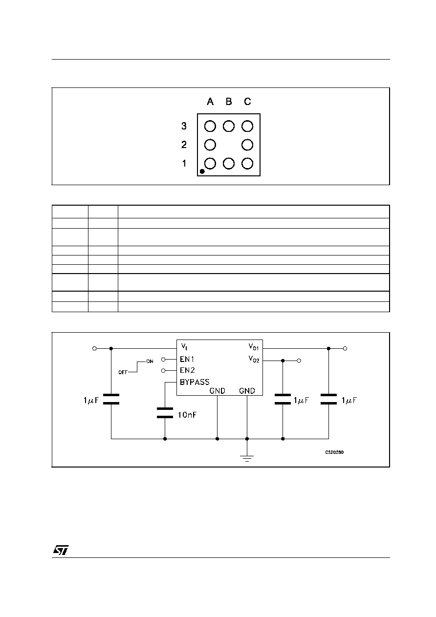
Figure 2: Pin Connection (top through view)
Table 4: Pin Description
Figure 3: Typical Application Circuit
Symbol
Pin N∞
Name and Function
V
O2
A1
Output Voltage 2 of the dual LDO
EN2
B1
Enables voltage for output voltage 2: ON MODE when V
EN
1.4V, OFF MODE when V
EN
0.4V (Do not leave floating, not internally pulled down/up)
BYPASS
C1
Bypass Pin: Connect an external capacitor (usually 10nF) to minimize noise voltage
GND
C2
Common Ground
GND
C3
Common Ground
EN1
B3
Enables voltage for output voltage 1: ON MODE when V
EN
1.4V, OFF MODE when V
EN
0.4V (Do not leave floating, not internally pulled down/up)
V
O1
A3
Output Voltage 1 of the dual LDO
V
I
A2
Input Voltage for both LDO

LD3986 SERIES
4/12
Table 5: Electrical Characteristics For LD3986 (T
j
= 25∞C, V
I
= V
O(NOM)
+0.5V, C
I
= C
O
=1
µ
F,
C
BYP
= 10nF, I
O
= 1mA, V
EN
= 1.4V, unless otherwise specified)
Symbol
Parameter
Test Conditions
Min.
Typ.
Max.
Unit
V
I
Operating Input Voltage
2.5
6
V
V
O
Output Voltage Tolerance
I
O
= 1mA
-2.5
2.5
% of V
O
T
J
= -40 to 125∞C
-3
3
V
O
Line Regulation (Note 1)
V
I
= V
O(NOM)
+ 0.5 V to 6V
0.006
0.092
%/V
T
J
= -40 to 125∞C
0.128
V
O
Load Regulation
I
O
= 1 mA to 150mA
0.003
0.006
%/mA
T
J
= -40 to 125∞C
0.01
V
O
Output AC Line Regulation
(See fig. 5)
V
I
= V
O(NOM)
+ 1 V, I
O
= 150mA,
t
R
= t
F
= 30µs
1.5
mV
PP
I
Q
Quiescent Current
BOTH ON MODE:
V
EN
= 1.4V
I
O
= 0
150
µA
I
O
= 0
T
J
= -40 to 125∞C
200
I
O
= 0 to 150mA
290
I
O
= 0 to 150mA
T
J
= -40 to 125∞C
370
BOTH OFF MODE:
V
EN
= 0.4V
0.001
2
T
J
= -40 to 125∞C
4
ONE REGULATOR
ON MODE: V
EN
= 1.4V
I
O
= 0
95
I
O
= 0
T
J
= -40 to 125∞C
130
I
O
= 0 to 150mA
165
I
O
= 0 to 150mA
T
J
= -40 to 125∞C
220
V
DROP
Dropout Voltage (Note 2)
I
O
= 1mA
0.4
mV
I
O
= 1mA
T
J
= -40 to 125∞C
2
I
O
= 150mA
50
I
O
= 150mA
T
J
= -40 to 125∞C
100
SVR
Supply Voltage Rejection
(See fig. 4)
V
I
= V
O(NOM)
+0.25V ±
V
RIPPLE
= 0.1V, I
O
= 50mA
V
O(NOM)
< 2.5V, V
I
= 2.55V
f = 1KHz
50
dB
f = 10KHz
40
I
SC
Short Circuit Current
R
L
= 0
600
mA
I
O(PK)
Peak Output Current
V
O
V
O(NOM)
- 5%
300
550
mA
V
EN
Enable Input Logic Low
(Note 3)
V
I
= 2.5V to 6V
T
J
= -40 to 125∞C
0.4
V
Enable Input Logic High
(Note 3)
1.4
I
EN
Enable Input Current
V
EN
= 0.4V
V
I
= 6V
±10
nA
X
TALK
Crosstalk Rejection
I
LOAD1
= 150 mA at 1KHz rate
I
LOAD2
= 1 mA, V
O2
under test
40
µV
I
LOAD2
= 150 mA at 1KHz rate
I
LOAD1
= 1 mA, V
O1
under test
40
eN
Output Noise Voltage
B
W
= 10 Hz to 100 KHz
C
O
= 1
µ
F
30
µ
V
RMS
t
ON
Turn On Time (Note 4)
C
BYP
= 10 nF
50
µ
s
T
SHDN
Thermal Shutdown (Note
4)
(Note 3)
160
∞C

LD3986 SERIES
5/12
Note 1: For V
O
< 2V, V
I
=2.5V
Note 2: Dropout voltage is the input-to-output voltage difference at which the output voltage is 100mV below its nominal value. This specifi-
cation does not apply for input voltages below 2.5V.
Note 3: Enable pin must be driven with a T
R
= T
F
< 10ms
Note 4: Turn-on time is time measured between the enable input just exceeding V
INH
High Value and the output voltage just reaching 95%
of its nominal value
Note 5: Typical thermal protection hysteresis is 20∞C
Figure 4: SVR Input Voltage Test Signal
Figure 5: AC Line Regulation Input Voltage Test Signal
C
O
Output Capacitor
Capacitance
1
22
µF
ESR
0.005
5
Symbol
Parameter
Test Conditions
Min.
Typ.
Max.
Unit
LD3986 SERIES
6/12
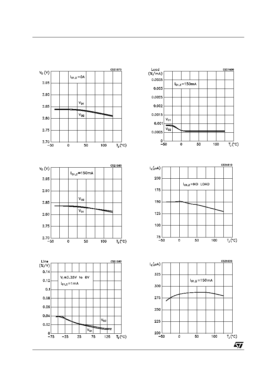
TYPICAL PERFORMANCE CHARACTERISTICS (T
j
= 25∞C, V
I
= V
O(NOM)
+0.5V, C
I
= C
O
= 1
µ
F,
C
BYP
= 1
0
nF, I
O
= 1mA, V
EN
= 1.4V, unless otherwise specified)
Figure 6: V
O1,2
vs Temperature
Figure 7: V
O1,2
vs Temperature
Figure 8: Line Regulation vs Temperature
Figure 9: Load Regulation vs Temperature
Figure 10: Quiescent Current vs Temperature
Figure 11: Quiescent Current vs Temperature
LD3986 SERIES
7/12
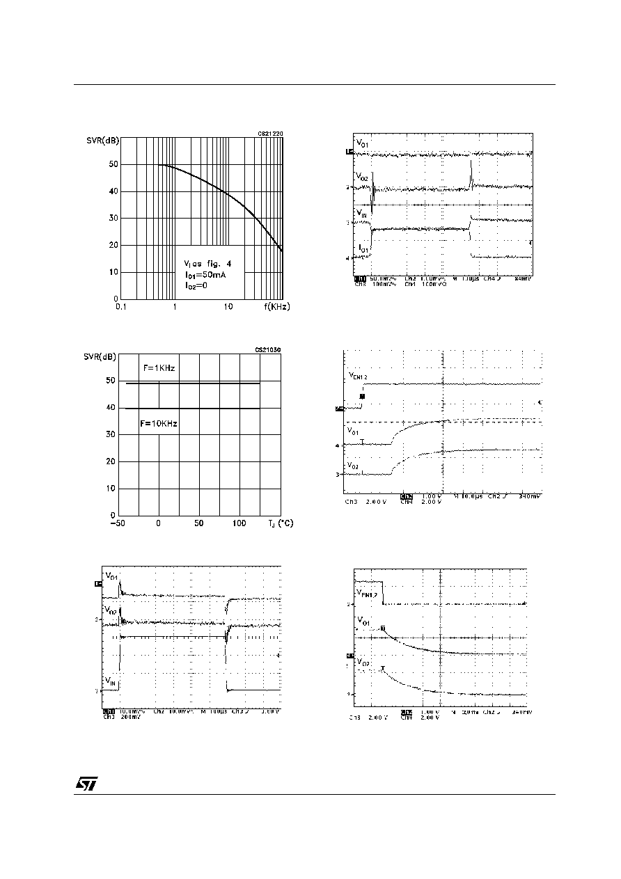
Figure 12: Supply Voltage Rejection vs
Frequency
Figure 13: Supply Voltage Rejection vs
Temperature
Figure 14: Line Transient Response
Figure 15: Load Transient Response
Figure 16: TURN-ON
Figure 17: TURN-OFF
V
I
= 3.2V to 3.8V, I
O1
= I
O2
= 150mA, T
R
= T
F
= 10
µ
s
I
O1
= 1 mA, I
O2
= 0mA, T
R
= T
F
= 10
µ
s
V
I
= 3.2V, V
EN1,2
= 0 to 1.4V, I
O1,2
= 1mA, T
R
= T
F
= 1
µ
s
V
I
= 3.2V, V
EN1,2
= 1.4 to 0V, I
O1,2
= 1mA, T
R
= T
F
= 1
µ
s

LD3986 SERIES
8/12
APPLICATION INFORMATION
CURRENT LIMIT
The device includes short-circuit protection. It
includes a current limiter that controls the pass
transistor's gate voltage to limit the output current
to about 600mA.
THERMAL OVERLOAD PROTECTION
The Thermal over load protection limits total
power dissipation in the device. When the junction
temperature (T
J
) exceeds +160∞C, the thermal
sensor sends a signal to the shutdown logic,
turning off the pass transistors and allowing the
device to cool. The pass transistors turns on again
after the device's junction temperature typically
cools by 20∞C, resulting in a pulsed output during
continuous thermal overload conditions.
POWER DISSIPATION
Maximum power dissipation of the device
depends on the thermal resistance of the case
and circuit board, the temperature difference
between the die junction and ambient air, and the
rate of air flow. The power dissipated by the
device is:
P
D
= I
O
(V
I
-V
O
)
The maximum power dissipation is:
P
MAX
= (T
JMAX
- T
A
) / R
TH
Where:
T
JMAX
= +125∞C
T
A
is the ambient temperature
R
TH
thermal resistance.
The device's pins perform the dual function of
providing an electrical connection as well as
channeling heat away from the die. Use wide
circuit-board traces and large, solid copper
polygons to improve power dissipation. Using
multiple vias to buried ground planes further
enhances thermal conductivity.
INPUT CAPACITOR
An input capacitance of
1µF is required between
the LD3986 input pin and ground (the amount of
the capacitance may be increased without limit).
This capacitor must be located a distance of not
more than 1cm from the input pin and returned to
a clean analog ground. Any good quality ceramic,
tantalum, or film capacitor may be used at the
input.
Important: Tantalum capacitors can suffer
catastrophic failures due to surge current when
connected to a low impedance source of power
(like a battery or a very large capacitor). If a
tantalum capacitor is used at the input, it must be
guaranteed by the manufacturer to have a surge
current rating sufficient for the application.
There are no requirements for the ESR on the
input capacitor, but tolerance and temperature
coefficient must be considered when selecting the
capacitor to ensure
the capacitance will be
1µF over the entire
operating temperature range.
OUTPUT CAPACITOR
The LD3986 is designed specifically to work with
very small ceramic output capacitors, any ceramic
capacitor (temperature characteristics X7R, X5R,
Z5U or Y5V) in 1 to 22 µF range with 5m. to 500m.
ESR range is suitable in the LD3986 application
circuit. it may also be possible to use tantalum or
film capacitors at the output, but these are not as
attractive for reasons of size and cost.
The output capacitor must meet the requirement
for minimum amount of capacitance and also have
an ESR (Equivalent Series Resistance) value
which is within a stable range.
NOISE BYPASS CAPACITOR
Connecting a 0.01µF capacitor between the C
BYP
pin and ground significantly reduces noise on both
regulator outputs.
This cap is connected directly to a high impedance
node in the band gap reference circuit. Any
significant loading on this node will cause a
change on the regulated output voltage.
For this reason, DC leakage current through this
pin must be kept as low as possible for best output
voltage accuracy. The use of this 0.01µF bypass
capacitor is strongly recommended to prevent
overshoot on the output during start up.
The types of capacitors best suited for the noise
bypass capacitor are ceramic and film.
High-quality ceramic capacitors with either NPO
or COG dielectric typically have very low leakage.
Polypropylene and polycarbonate film capacitors
are available in small surface-mount packages
and typically have extremely low leakage current.
Unlike many other LDO's, addition of a noise
reduction capacitor does not effect the transient
response of the device.
TURN-ON/OFF INPUT OPERATION
Each LD3986 output is turned off by pulling the
relevant EN pin low, and turned on by pulling it
high. To assure proper operation, the signal

LD3986 SERIES
9/12
source used to drive the EN input must be able to
swing above and below the specified turn-on/off
voltage thresholds listed in the Electrical
Characteristics section under Enable Input Logic
Low and Enable Input Logic High.
Proper operation of the Enable function is
guaranteed by driving EN pins with T
R
and T
F
= 10
ms.
FAST ON-TIME
The LD3986 outputs are turned on after V
REF
voltage reaches its final value (1.23V nominal). To
speed up this process, the noise reduction
capacitor at the bypass pin is charged with an
internal 70µA current source. The current source
is turned off when the bandgap voltage reaches
approximately 95% of its final value. The turn on
time is determined by the time constant of the
bypass capacitor. The smaller the capacitor value,
the shorter the turn on time, but less noise gets
reduced. As a result, turn on time and noise
reduction need to be taken into design
consideration when choosing the value of the
bypass capacitor.
LD3986 SERIES
10/12
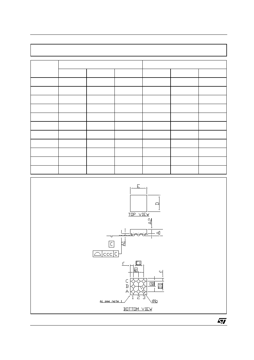
DIM.
mm.
mils
MIN.
TYP
MAX.
MIN.
TYP.
MAX.
A
0.585
0.65
0.715
23.0
25.6
28.1
A1
0.21
0.25
0.29
8.3
9.8
11.4
A2
0.40
15.7
b
0.265
0.315
0.365
10.4
12.4
14.4
D
1.52
1.57
1.62
59.8
61.8
63.8
D1
1
39.4
E
1.52
1.57
1.62
59.8
61.8
63.8
E1
1
39.4
e
0.45
0.5
0.55
17.7
19.7
20.7
f
0.285
11.2
ccc
0.080
3.1
Flip-Chip8 MECHANICAL DATA
7224720E
LD3986 SERIES
11/12
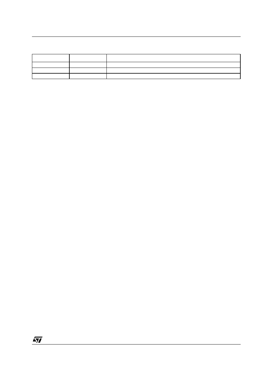
Table 6: Revision History
Date
Revision
Description of Changes
07-Dec-2004
1
First Release.
06-Jun-2005
2
Add New Part Number - Table 1.
22-Sep-2005
3
Order Codes has been updated.

LD3986 SERIES
12/12
Information furnished is believed to be accurate and reliable. However, STMicroelectronics assumes no responsibility for the consequences
of use of such information nor for any infringement of patents or other rights of third parties which may result from its use. No license is granted
by implication or otherwise under any patent or patent rights of STMicroelectronics. Specifications mentioned in this publication are subject
to change without notice. This publication supersedes and replaces all information previously supplied. STMicroelectronics products are not
authorized for use as critical components in life support devices or systems without express written approval of STMicroelectronics.
The ST logo is a registered trademark of STMicroelectronics
All other names are the property of their respective owners
© 2005 STMicroelectronics - All Rights Reserved
STMicroelectronics group of companies
Australia - Belgium - Brazil - Canada - China - Czech Republic - Finland - France - Germany - Hong Kong - India - Israel - Italy - Japan -
Malaysia - Malta - Morocco - Singapore - Spain - Sweden - Switzerland - United Kingdom - United States of America
www.st.com