 | –≠–ª–µ–∫—Ç—Ä–æ–Ω–Ω—ã–π –∫–æ–º–ø–æ–Ω–µ–Ω—Ç: L6910ATR | –°–∫–∞—á–∞—Ç—å:  PDF PDF  ZIP ZIP |

1/21
L6910
L6910A
July 2003
FEATURE
s
OPERATING SUPPLY VOLTAGE FROM 5V
TO 12V BUSES
s
UP TO 1.3A GATE CURRENT CAPABILITY
s
ADJUSTABLE OUTPUT VOLTAGE
s
N-INVERTING E/A INPUT AVAILABLE
s
0.9V ±1.5% VOLTAGE REFERENCE
s
VOLTAGE MODE PWM CONTROL
s
VERY FAST LOAD TRANSIENT RESPONSE
s
0% TO 100% DUTY CYCLE
s
POWER GOOD OUTPUT
s
OVERVOLTAGE PROTECTION
s
HICCUP OVERCURRENT PROTECTION
s
200kHz INTERNAL OSCILLATOR
s
OSCILLATOR EXTERNALLY ADJUSTABLE
FROM 50kHz TO 1MHz
s
SOFT START AND INHIBIT
s
PACKAGES: SO-16 & HTSSOP16
APPLICATIONS
s
SUPPLY FOR MEMORIES AND TERMI-
NATIONS
s
COMPUTER ADD-ON CARDS
s
LOW VOLTAGE DISTRIBUTED DC-DC
s
MAG-AMP REPLACEMENT
DESCRIPTION
The device is a pwm controller for high performance
dc-dc conversion from 3.3V, 5V and 12V buses.
The output voltage is adjustable down to 0.9V; higher
voltages can be obtained with an external voltage di-
vider.
High peak current gate drivers provide for fast switch-
ing to the external power section, and the output
current can be in excess of 20A.
The device assures protections against load overcur-
rent and overvoltage. An internal crowbar is also pro-
vided turning on the low side mosfet as long as the
over-voltage is detected. In case of over-current de-
tection, the soft start capacitor is discharged and the
system works in HICCUP mode.
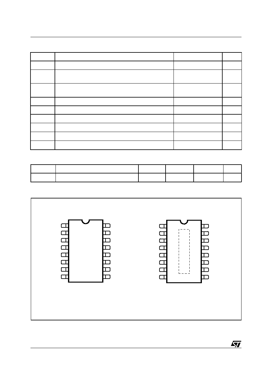
SO-16 (Narrow)
HTSSOP16 (Exposed Pad)
ORDERING NUMBERS:
L6910 (SO-16)
L6910A (HTSSOP16)
L6910TR (Tape & Reel) L6910ATR (Tape & Reel)
ADJUSTABLE STEP DOWN CONTROLLER
WITH SYNCHRONOUS RECTIFICATION
BLOCK DIAGRAM
L6910
PGND
PHASE
GND
VFB
LGATE
BOOT
UGATE
VCC
OCSET
Vin 5V to12V
Vo
PGOOD
COMP
SS
Monitor
Protection and Ref
OSC
+
-
+
-
E/A
PWM
EAREF
OSC
VREF
300k
R
T
L6910A L6910
2/21
ABSOLUTE MAXIMUM RATINGS
THERMAL DATA
(*) Device soldered on 1 S2P PC board
PINS CONNECTION (Top view)
Symbol
Parameter
Value
Unit
Vcc
Vcc to GND, PGND
15
V
V
BOOT
-
V
PHASE
Boot Voltage
15
V
V
HGATE
-
V
PHASE
15
V
OCSET, LGATE, PHASE
-0.3 to Vcc+0.3
V
SS, FB, PGOOD, VREF, EAREF, RT
7
V
COMP
6.5
V
T
j
Junction Temperature Range
-40 to 150
∞
C
T
stg
Storage temperature range
-40 to 150
∞
C
P
tot
Maximum power dissipation at Tamb = 25
∞
C
1
W
Symbol
Parameter
SO-16
HTSSOP16
HTSSOP16 (*)
Unit
R
th j-amb
Thermal Resistance Junction to Ambient
120
110
50
∞
C/W
VREF
OSC
OCSET
SS/INH
COMP
GND
FB
EAREF
PGOOD
PHASE
BOOT
HGATE
PGND
LGATE
VCC
N.C.
1
3
2
4
5
6
7
8
14
13
12
11
10
9
15
16
SO16
VREF
OSC
OCSET
SS/INH
N.C.
FB
COMP
GND
EAREF
PGOOD
HGATE
PHASE
BOOT
PGND
LGATE
VCC
1
3
2
4
5
6
7
8
14
13
12
11
10
9
15
16
HTSSOP-16

3/21
L6910A L6910
PINS FUNCTION
SO
HTSSOP
Name
Description
1
1
VREF
Internal 0.9V ±1.5% reference is available for external regulators or for the internal error
amplifier (connecting this pin to EAREF) if external reference is not available.
A minimum 1nF capacitor is required.
If the pin is forced to a voltage lower than 70%, the device enters the hiccup mode.
2
2
OSC
Oscillator switching frequency pin. Connecting an external resistor (R
T
) from this pin to
GND, the external frequency is increased according to the equation:
Connecting a resistor (R
T
) from this pin to Vcc (12V), the switching frequency is reduced
according to the equation:
If the pin is not connected, the switching frequency is 200KHz.
The voltage at this pin is fixed at 1.23V. Forcing a 50
µ
A current into this pin, the built in
oscillator stops to switch.
In Over Voltage condition this pin goes over 3V until that conditon is removed.
3
3
OCSET
A resistor connected from this pin and the upper Mos Drain sets the current limit
protection.
The internal 200
µ
A current generator sinks a constant current through the external
resistor. The Over-Current threshold is due to the following equation:
4
4
SS/INH
The soft start time is programmed connecting an external capacitor from this pin and
GND. The internal current generator forces through the capacitor 10
µ
A.
This pin can be used to disable the device forcing a voltage lower than 0.4V
5
6
COMP
This pin is connected to the error amplifier output and is used to compensate the voltage
control feedback loop.
6
7
FB
This pin is connected to the error amplifier inverting input and is used to compensate the
voltage control feedback loop.
Connected to the output resistor divider, if used, or directly to Vout, it manages also over-
voltage conditions and the PGOOD signal
7
8
GND
All the internal references are referred to this pin. Connect it to the PCB signal ground.
8
9
EAREF
Error amplifier non-inverting input. Connect to this pin an external reference (from 0.9V to
3V) for the PWM regulation or short it to VREF pin to use the internal reference.
If this pin goes under 650mV (typ), the device shuts down.
9
10
PGOOD This pin is an open collector output and it is pulled low if the output voltage is not within the
above specified thresholds. If not used it may be left floating.
10
11
PHASE
This pin is connected to the source of the upper mosfet and provides the return path for the
high side driver. This pin monitors the drop across the upper mosfet for the current limit
together with OCSET.
11
12
HGATE
High side gate driver output.
12
13
BOOT
Bootstrap capacitor pin. Through this pin is supplied the high side driver and the upper
mosfet. Connect through a capacitor to the PHASE pin and through a diode to Vcc
(cathode vs. boot).
13
14
PGND
Power ground pin. This pin has to be connected closely to the low side mosfet source in
order to reduce the noise injection into the device
14
`5
LGATE
This pin is the lower mosfet gate driver output
15
16
VCC
Device supply voltage. The operative supply voltage ranges is from 5V to 12V.
DO NOT CONNECT V
IN
TO A VOLTAGE GREATER THAN V
CC
.
16
5
N.C.
This pin is not internally bonded. It may be left floating or connected to GND.
f
O SC ,RT
200KHz
4.94 10
6
R
T
K
(
)
-------------------------
+
=
f
O SC ,RT
200KHz
4.306 10
7
R
T
K
(
)
-----------------------------
≠
=
I
P
I
OC SE T
R
O CS ET
R
DS on
----------------------------------------------
=
L6910A L6910
4/21
ELECTRICAL CHARACTERISTICS (V
cc
= 12V, T
J
=25∞C unless otherwise specified)
Symbol
Parameter
Test Condition
Min
Typ
Max
Unit
V
cc
SUPPLY CURRENT
Icc
Vcc Supply current
OSC = open; SS to GND
4
7
9
mA
POWER-ON
Turn-On Vcc threshold
VOCSET = 4V
4.0
4.3
4.6
V
Turn-Off Vcc threshold
VOCSET = 4V
3.8
4.1
4.4
V
Rising V
OCSET
threshold
1.24
1.4
V
Turn On EAREF threshold
VOCSET = 4V
650
750
mV
SOFT START AND INHIBIT
Iss
Soft start Current
S.S. current in INH condition
SS = 2V
SS = 0 to 0.4V
6
10
35
14
60
µ
A
µ
A
OSCILLATOR
f
OSC
Initial Accuracy
OSC = OPEN
OSC = OPEN; T
j
= 0
∞
to 125
∞
180
170
200
220
230
KHz
kHz
f
OSC,RT
Total Accuracy
16 K
< R
T
to GND < 200 K
-15
15
%
Vosc
Ramp amplitude
1.9
V
REFERENCE
V
OUT
Output Voltage Accuracy
V
OUT
= V
FB
; V
EAREF
= V
REF
0.886
0.900
0.913
V
V
REF
Reference Voltage
C
REF
= 1nF; I
REF
= 0 to 100
µ
A
0.886
0.900
0.913
V
V
REF
Reference Voltage
C
REF
= 1nF; T
J
= 0 to 125
∞
C
-2
+2
%
ERROR AMPLIFIER
I
EAREF
N.I. bias current
V
EAREF
= 3V
10
µ
A
EAREF Input Resistance
Vs. GND
300
k
I
FB
I.I. bias current
V
FB
= 0V to 3V
0.01
0.5
µ
A
V
CM
Common Mode Voltage
0.8
3
V
V
COMP
Output Voltage
0.5
4
V
G
V
Open Loop Voltage Gain
70
85
dB
GBWP
Gain-Bandwidth Product
10
MHz
SR
Slew-Rate
COMP = 10pF
10
V/
µ
s
GATE DRIVERS
I
HGATE
High Side
Source Current
V
BOOT
- V
PHASE
= 12V
V
HGATE
- V
PHASE
= 6V
1
1.3
A
R
HGATE
High Side
Sink Resistance
V
BOOT
- V
PHASE
= 12V
2
4
I
LGATE
Low Side Source Current
Vcc = 12V; V
LGATE
= 6V
0.9
1.1
A
R
LGATE
Low Side Sink Resistance
Vcc = 12V
1.5
3
Output Driver Dead Time
PHASE connected to GND
90
210
ns
PROTECTIONS
I
OCSET
OCSET Current Source
V
OCSET
= 4V
170
200
230
µ
A
Over Voltage Trip (V
FB
/ V
EAREF
)
V
FB
Rising
117
120
%
I
OSC
OSC Sourcing Current
V
FB
> OVP Trip
15
30
mA
POWER GOOD
Upper Threshold (V
FB
/ V
EAREF
)
V
FB
Rising
108
110
112
%
Lower Threshold (V
FB
/ V
EAREF
)
V
FB
Falling
88
90
92
%
Hysteresis (V
FB
/ V
EAREF
)
Upper and Lower threshold
2
%
V
PGOOD
PGOOD Voltage Low
I
PGOOD
= -4mA
0.4
V
I
PGOOD
Output Leakage Current
V
PGOOD
= 6V
0.2
1
µ
A

5/21
L6910A L6910
Device Description
The device is an integrated circuit realized in BCD technology. The controller provides complete control logic and
protection for a high performance step-down DC-DC converter. It is designed to drive N Channel Mosfets in a
synchronous-rectified buck topology. The output voltage of the converter can be precisely regulated down to
900mV with a maximum tolerance of ±1.5% when the internal reference is used (simply connecting together
EAREF and VREF pins). The device allows also using an external reference (0.9V to 3V) for the regulation. The
device provides voltage-mode control with fast transient response. It includes a 200kHz free-running oscillator that
is adjustable from 50kHz to 1MHz. The error amplifier features a 10MHz gain-bandwidth product and 10V/
µ
s slew
rate that permits to realize high converter bandwidth for fast transient performance. The PWM duty cycle can
range from 0% to 100%. The device protects against over-current conditions entering in HICCUP mode. The de-
vice monitors the current by using the r
DS(ON)
of the upper MOSFET(s) that eliminates the need for a current
sensing resistor. The device is available in SO16 narrow package.
Oscillator
The switching frequency is internally fixed to 200kHz. The internal oscillator generates the triangular waveform
for the PWM charging and discharging with a constant current an internal capacitor. The current delivered to the
oscillator is typically 50
µ
A (F
sw
= 200KHz) and may be varied using an external resistor (R
T
) connected between
OSC pin and GND or V
CC
. Since the OSC pin is maintained at fixed voltage (typ. 1.235V), the frequency is var-
ied proportionally to the current sunk (forced) from (into) the pin.
In particular connecting R
T
vs. GND the frequency is increased (current is sunk from the pin), according to the
following relationship:
Connecting R
T
to V
CC
= 12V or to V
CC
= 5V the frequency is reduced (current is forced into the pin), according
to the following relationships:
V
CC
= 12V
V
CC
= 5V
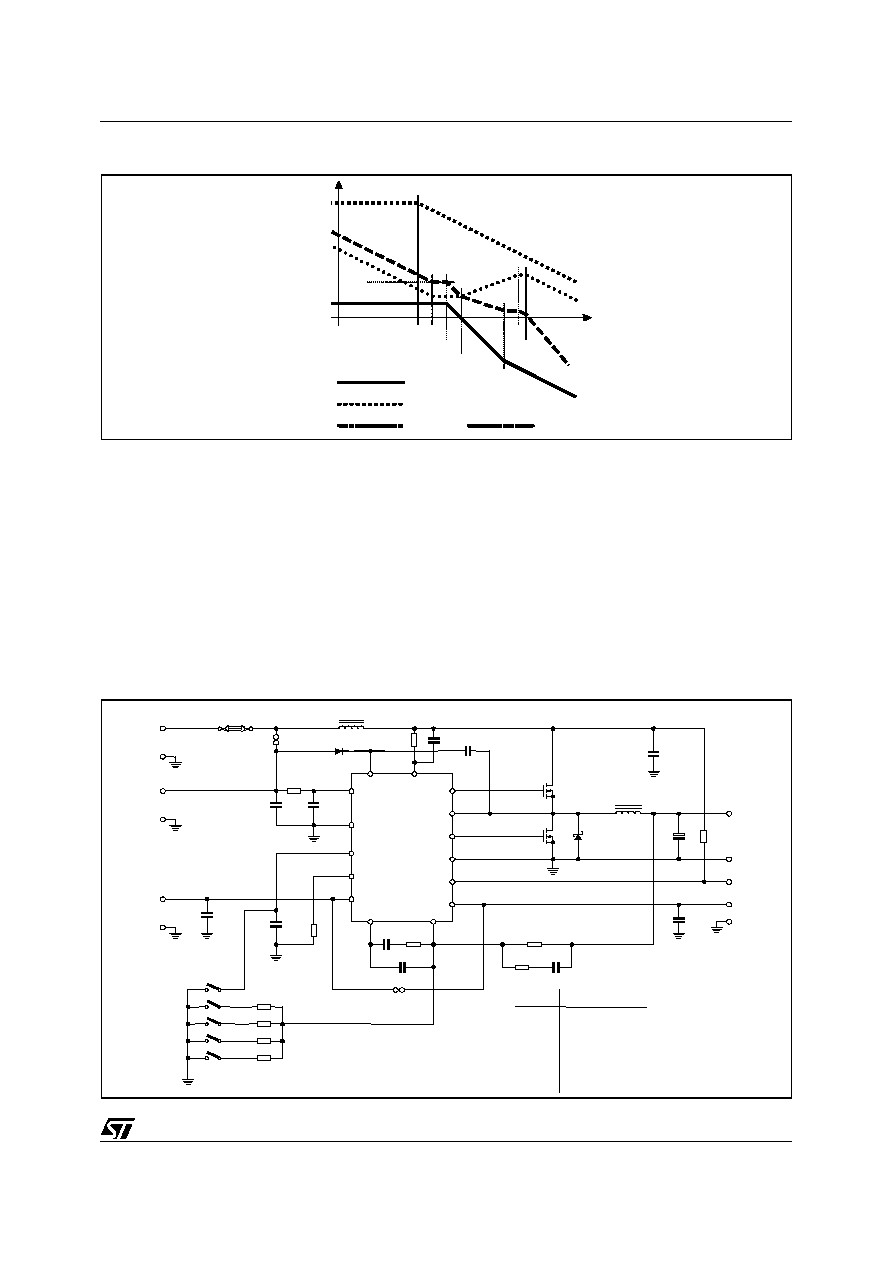
Switching frequency variation vs. RT are repeated in Fig. 1.
Note that forcing a 50
µ
A current into this pin, the device stops switching because no current is delivered to the
oscillator.
f
O SC ,RT
200KH z
4.94 10
6
R
T
K
(
)
-------------------------
+
=
f
O SC ,RT
200KH z
4.306 10
7
R
T
K
(
)
-----------------------------
≠
=
f
O SC ,RT
200KH z
15 10
6
R
T
K
(
)
---------------------
≠
=
Figure 1.
Reference
A precise ±1.5% 0.9V reference is available. This ref-
erence must be filtered with 1nF ceramic capacitor to
avoid instability in the internal linear regulator. It is
able to deliver up to 100
µ
A and may be used as ref-
erence for the device regulation and also for other de-
vices. If forced under 70% of its nominal value, the
device enters in Hiccup mode until this condition is
removed.
Through the EAREF pin the reference for the regula-
tion is taken. This pin directly connects the non-in-
verting input of the error amplifier. An external
reference (or the internal 0.9V ±1.5%) may be used.
The input for this pin can range from 0.9V to 3V. It
has an internal pull-down (300k
resistor) that forces
the device shutdown if no reference is connected (pin
floating). However the device is shut down if the volt-
age on the EAREF pin is lower than 650mV (typ).
10
100
1000
Frequency [kHz]
10
100
1000
10000
R
e
si
st
ance [
k
O
h
m
]
RT to GND
RT to VCC=12V
RT to VCC=5V

L6910A L6910
6/21
Soft Start
At start-up a ramp is generated charging the external capacitor C
SS
with an internal current generator. The initial
value for this current is of 35
µ
A and speeds-up the charge of the capacitor up to 0.5V. After that it becames
10
µ
A until the final charge value of approximatively 4V.
When the voltage across the soft start capacitor (V
SS
) reaches 0.5V the lower power MOS is turned on to dis-
charge the output capacitor. As V
SS
reaches 1.1V (i.e. the oscillator triangular wave inferior limit) also the upper
MOS begins to switch and the output voltage starts to increase.
No switching activity is observable if SS is kept lower than 0.5V and both mosfets are off.
If VCC and OCSET pins are not above their own turn-on thresholds and V
EAREF
is not above 650mV, the Soft-
Start will not take place, and the relative pin is internally shorted to GND. During normal operation, if any under-
voltage is detected on one of the two supplies, the SS pin is internally shorted to GND and so the SS capacitor
is rapidly discharged.
Figure 2. Soft Start (with Reference Present)
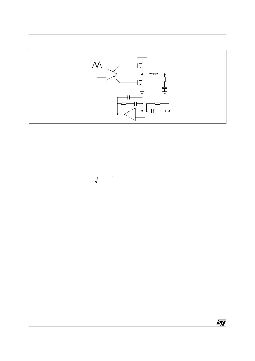
Driver Section
The driver capability on the high and low side drivers allows using different types of power MOS (also multiple
MOS to reduce the R
DSON
), maintaining fast switching transition.
The low-side mos driver is supplied directly by Vcc while the high-side driver is supplied by the BOOT pin.
Adaptative dead time control is implemented to prevent cross-conduction and allow to use several kinds of mos-
fets. The upper mos turn-on is avoided if the lower gate is over about 200mV while the lower mos turn-on is
avoided if the PHASE pin is over about 500mV. The lower mos is in any case turned-on after 200ns from the
high side turn-off.
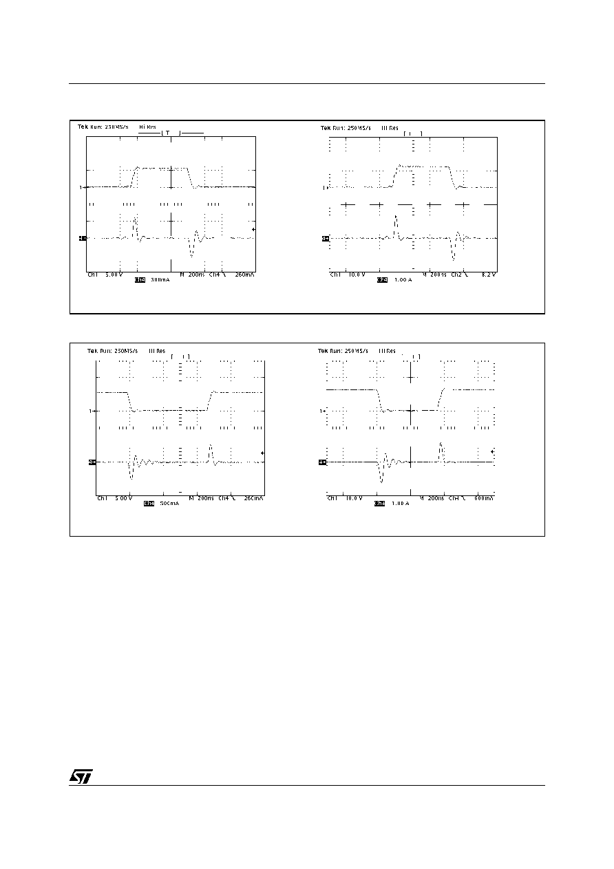
The peak current is shown for both the upper (fig. 3) and the lower (fig. 4) driver at 5V and 12V. A 3.3nF capac-
itive load has been used in these measurements.
For the lower driver, the source peak current is 1.1A @ V
CC
= 12V and 500mA @ V
CC
= 5V, and the sink peak
current is 1.3A @ V
CC
= 12V and 500mA @ V
CC
= 5V.
Similarly, for the upper driver, the source peak current is 1.3A @ Vboot-Vphase = 12V and 600mA @ Vboot-
Vphase = 5V, and the sink peak current is 1.3A @ Vboot-Vphase =12V and 550mA @ Vboot-Vphase = 5V.
Timing Diagram
Vcc Turn-on threshold
Vin Turn-on threshold
0.5V
1V
Vcc
Vin
Vss
LGATE
Vout
to GND
Acquisition: CH1 = PHASE; CH2 = V
out
;
CH3 = PGOOD; CH4 = V
ss
7/21
L6910A L6910
Figure 3. High Side driver peak current. Vboot-Vphase = 12V (right) Vboot-Vphase = 5V (left)
Figure 4. Low Side driver peak current. V
CC
= 12V (right) V
CC
= 5V (left)
Monitoring and Protections
The output voltage is monitored by means of pin FB. If it is not within ±10% (typ.) of the programmed value, the
powergood output is forced low.
The device provides overvoltage protection, when the voltage sensed on pin FB reaches a value 17% (typ.)
greater than the reference the OSC pin is forced high (3V typ.) and the lower driver is turned on as long as the
over-voltage is detected.
Overcurrent protection is performed by the device comparing the drop across the high side MOS, due to the
R
DSON
, with the voltage across the external resistor (R
OCS
) connected between the OCSET pin and drain of the
upper MOS. Thus the overcurrent threshold (I
P
) can be calculated with the following relationship:
Where the typical value of I
OCS
is 200
µ
A. To calculate the R
OCS
value it must be considered the maximum
R
dsON
(also the variation with temperature) and the minimum value of I
OCS
. To avoid undesirable trigger of
overcurrent protection this relationship must be satisfied:
CH1 = High Side Gate CH4 = Gate Current
CH1 = Low Side Gate CH4 = Gate Current
I
P
R
O C S
I
O C S
R
ds O N
---------------------------------
=

L6910A L6910
8/21
Where
I is the inductance ripple current and I
OUTMAX
is the maximum output current.
In case of over current detectionthe soft start capacitor is discharged with constant current (10
µ
A typ.) and when
the SS pin reaches 0.5V the soft start phase is restarted. During the soft start the over-current protection is al-
ways active and if such kind of event occurs, the device turns off both mosfets, and the SS capacitor is dis-
charged again (after reaching the upper threshold of about 4V). The system is now working in HICCUP mode,
as shown in figure 5. After removing the cause of the over-current, the device restart working normally without
power supplies turn off and on.
I
P
I
O U T MAX
I
2
-----
+
I
PE AK
=
Figure 5. Hiccup Mode
Figure 6. Inductor ripple current vs. Vout
CH1 = SS; CH4 = Inductor current
0
1
2
3
4
5
6
7
8
9
0 .5
1.5
2.5
3 .5
Output V oltage [V ]
Inductor Ripple [A]
L=3
µ
H,
Vin=12V
L=2
µ
H,
Vin=12V
L=1.5
µ
H, Vin=12V
L=2
µ
H,
Vin=5V
L=1.5
µ
H,
Vin=5V
L=3
µ
H, Vin=5V
Inductor design
The inductance value is defined by a compromise between the transient response time, the efficiency, the cost
and the size. The inductor has to be calculated to sustain the output and the input voltage variation to maintain
the ripple current
I
L
between 20% and 30% of the maximum output current. The inductance value can be cal-
culated with this relationship:
Where f
SW
is the switching frequency, V
IN
is the input voltage and V
OUT
is the output voltage. Figure 6 shows
the ripple current vs. the output voltage for different values of the inductor, with V
IN
= 5V and V
IN
= 12V.
Increasing the value of the inductance reduces the ripple current but, at the same time, reduces the converter
response time to a load transient. If the compensation network is well designed, the device is able to open or
close the duty cycle up to 100% or down to 0%. The response time is now the time required by the inductor to
change its current from initial to final value. Since the inductor has not finished its charging time, the output cur-
rent is supplied by the output capacitors. Minimizing the response time can minimize the output capacitance
required.
The response time to a load transient is different for the application or the removal of the load: if during the ap-
plication of the load the inductor is charged by a voltage equal to the difference between the input and the output
voltage, during the removal it is discharged only by the output voltage. The following expressions give approx-
imate response time for
I load transient in case of enough fast compensation network response:
The worst condition depends on the input voltage available and the output voltage selected. Anyway the worst
case is the response time after removal of the load with the minimum output voltage programmed and the max-
imum input voltage available.
L
V
IN
V
O U T
≠
f
s w
I
L
------------------------------
V
OU T
V
IN
---------------
=
t
a pplic atio n
L
I
V
IN
V
O U T
≠
------------------------------
t
rem ov al
L
I
V
O U T
---------------
=
=

9/21
L6910A L6910
Output Capacitor
The output capacitor is a basic component for the fast response of the power supply. In fact, during load tran-
sient, for first few microseconds they supply the current to the load. The controller recognizes immediately the
load transient and sets the duty cycle at 100%, but the current slope is limited by the inductor value. The output
voltage has a first drop due to the current variation inside the capacitor (neglecting the effect of the ESL):
A minimum capacitor value is required to sustain the current during the load transient without discharge it. The
voltage drop due to the output capacitor discharge is given by the following equation:
Where D
MAX
is the maximum duty cycle value that is 100%. The lower is the ESR, the lower is the output drop
during load transient and the lower is the output voltage static ripple.
Input Capacitor
The input capacitor has to sustain the ripple current produced during the on time of the upper MOS, so it must
have a low ESR to minimize the losses. The rms value of this ripple is:
Where D is the duty cycle. The equation reaches its maximum value with D = 0.5. The losses in worst case are:
Compensation network design
The control loop is a voltage mode (figure 7). The output voltage is regulated to the input Reference voltage
level (EAREF). The error amplifier output V
COMP
is then compared with the oscillator triangular wave to provide
a pulse-width modulated (PWM) wave with an amplitude of V
IN
at the PHASE node. This wave is filtered by the
output filter. The modulator transfer function is the small-signal transfer function of V
OUT
/V
COMP
. This function
has a double pole at frequency F
LC
depending on the L-C
out
resonance and a zero at F
ESR
depending on the
output capacitor ESR. The DC Gain of the modulator is simply the input voltage V
IN
divided by the peak-to-peak
oscillator voltage
V
OSC
.
V
O U T
I
O U T
ESR
=
V
O U T
I
O U T
2
L
2 C
O U T
V
IN M IN
D
M AX
V
O U T
≠
(
)
---------------------------------------------------------------------------------------------
=
I
rm s
I
O U T
D
1
D
≠
(
)
=
P
ESR I
rm s
2
=
L6910A L6910
10/21
Figure 7. Compensation Network
The compensation network consists in the internal error amplifier and the impedance networks Z
IN
(R3, R4 and
C20) and Z
FB
(R5, C18 and C19). The compensation network has to provide a closed loop transfer function with
the highest 0dB crossing frequency to have fast response (but always lower than fsw/10) and the highest gain
in DC conditions to minimize the load regulation.
A stable control loop has a gain crossing with -20dB/decade slope and a phase margin greater than 45∞. Include
worst-case component variations when determining phase margin.
To locate poles and zeroes of the compensation networks, the following suggestions may be used:
Modulator singularity frequencies:
Compensation network singularity frequency:
≠ Put the gain R5/R3 in order to obtain the desired converter bandwidth;
≠ Place
Z1
before the output filter resonance
LC
;
≠ Place
Z2
at the output filter resonance
LC
;
≠ Place
P1
at the output capacitor ESR zero
ESR
;
≠ Place
P2
at one half of the switching frequency;
≠ Check the loop gain considering the error amplifier open loop gain.
Vin
L
ESR
Cout
R3
R5
C19
EAREF
Vcomp
PWM
Comparator
Vout
Vosc
R4
C18
C20
+
-
LC
1
L C
O U T
---------------------------
ESR
1
ESR C
O U T
---------------------------------
=
=
P1
1
R5
C18 C19
C 18
C 19
+
-----------------------------
-----------------------------------------------
P2
1
R4 C 20
------------------------
=
=
Z1
1
R5 C19
------------------------
Z2
1
R3
R 4
+
(
)
C20
-------------------------------------------
=
=
11/21
L6910A L6910
Figure 8. Asymptotic Bode plot of Converter's gain
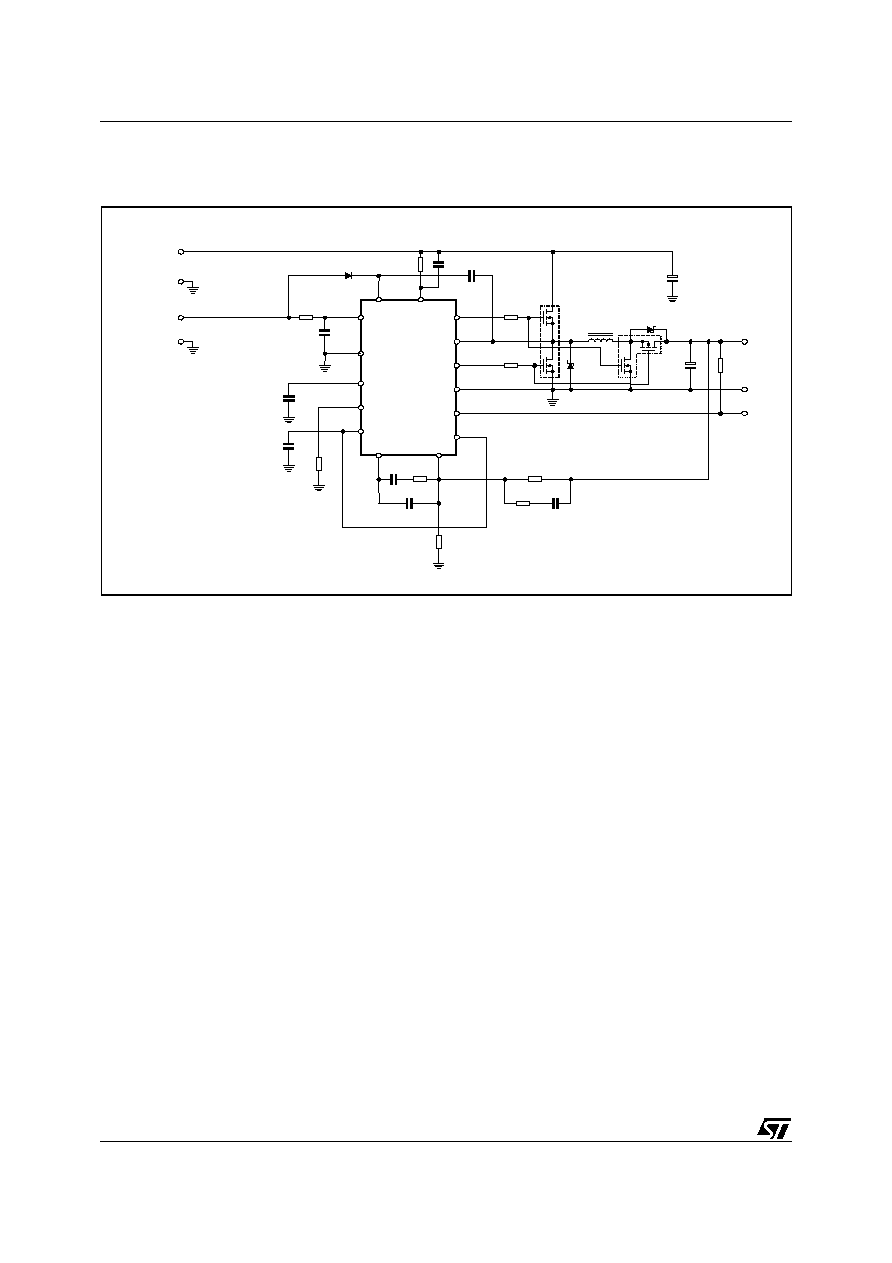
20A Demo Board Description
The demo board shows the operation of the device in a general purpose application. This evaluation board al-
lows voltage adjustability from 0.9V to 5V through the switches S2-S5 according to the reported table when the
internal 0.9V reference is used (G1 closed). Output current in excess of 20A can be reached dependently on
the kind of mosfet used: up to three SO8 mosfet may be used for both High side and Low side switches. External
reference may be used for the regulation simply leaving open G1 and the switches S2-S5. The device may also
be disabled with the switch S1. The 12V input rail supplies the device while the power conversion starts from
the 5V input rail. The device is also able to operate with a single supply voltage; in this case the jumper G2 has
to be closed and a 5V to 12V input can be directly connected to the V
IN
input. The four layers demo board's
copper thickness is of 70
µ
m in order to minimize conduction losses considering the high current that the circuit
is able to deliver. Figure 9 shows the demo board's schematic circuit
Figure 9. 20A Demo Board Schematic
Error Amplifier
1
2
P1
P2
ESR
R5/R3
Modulator Gain
Compensation Network Gain
Error Amplifier
Closed Loop Gain
LC
dB
L2
L1
R7
C1 -C3
C14
C4 -11
Q4 -6
Q1 -3
D2
C17
F1
13
14
10
11
3
1
U1
L6910
VIN
VOUT
PWRGD
6
12
5
4
2
15
7
9
VCC
GND
VREF
SS
OSC
OCSET
UGATE
PHASE
LGATE
PGND
PGOOD
V
F
B
CO
M
P
C19
R1
C21
C13
D1
GNDIN
GNDOU T
R2
GNDref
+Vref
C12
GNDRef
IN
Ref
IN
C16
G1
C15
R6
C18
8
GNDCC
VCC
R5
G2
R3
R4
C20
S1
S2
S3
S4
S5
R10
R11
R12
R13
EAREF
BOOT
Vout
S2
S3
S4
S5
0.9
1.2
1.5
1.8
2.5
3.3
5.0
Open
Open
ON
Ope n
Open
Open
Open
Open
Open
Open
Open
Open
Open
Open
Open
Open
Open
ON
ON
ON
Open
Open
ON
ON
ON
ON
Open
Open
L6910A L6910
12/21
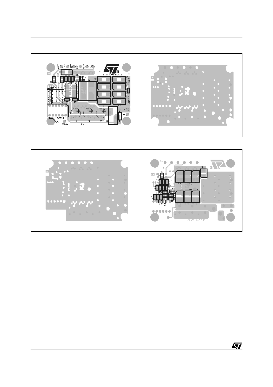
Figure 10. PCB and Components Layouts
Figure 11. PCB and Components Layouts
Figures 10 and 11 show the demo board layout.
Considering the flexibility in the power mosfet configuration (up to three mosfet for both high side and low side),
it is possible to obtain different application idea with the same board.
In the following paragraphs, it will be described the standard demo-board configuration (8A) and the high current
configuration.
APPLICATION IDEA: 5V TO 12V INPUT; 0.9V TO 5V / 8A OUTPUT
This is a typical bus termination application in which the output voltage is programmed by the switch to 1.2V typ
(it can range from 0.9V to 5V) and the maximum output current is of 8A DC. The power mosfet are configured
with one STS12NF30L (30V, 10m
typ @ Vgs=4.5V ) for both hgih side and low side.
Inductor selection
Since the maximum output current is 8A, to have a 15% ripple (1A) in worst case the inductor chosen is 4.1
µ
H.
SUMIDA CEE125 series inductor has been chosen with a 4.2
µ
A typical value.
Component Side
Internal Signal GND Layer
Internal Power GND Layer
Solder Side
13/21
L6910A L6910
Output Capacitor
In the demo 5 POSCAP capacitors, model 6TPB330M, are used, with a maximum ESR equal to 40m
each.
Therefore the resultant ESR is of 8m
. For load transient of 8A in the worst case the voltage drop is of:
V
out
= 8 ∑ 0.008 = 64mV
The voltage drop due to the capacitor discharge during load transient, considering that the maximum duty cycle
is equal to 100% results in 16.4mV with 1.2V of programmed output.
Input Capacitor
For I
OUT
= 8A and D=0.5 (worst case for input ripple current), Irms is equal to 4A. Three OSCON electrolytic
capacitors 20SA100M, with a maximum ESR equal to 30m
, are chosen to sustain the ripple. Therefore, the
resultant ESR is equal to 30m
/3 = 10m
. So the losses in worst case are:
P = ESR ∑
= 160mW
Over-Current Protection
The peak current is in this case equal to 12A, substituting the demo board parameters in the relationship report-
ed in the relative section, (I
OCSMIN
= 170
µ
A; I
P
= 12A; R
DSONMAX
= 9m
) it results that R
OCS
= 620
.
Efficiency
Figure 12 shows the measured efficiency versus load current for different values of output voltage. The measure
was done at V
in
= 5V for different values of the output voltage (0.9V, 1.2V, 1.5V, 1.8V, 2.5V and 3.3V). IC supply
voltage is of 12V.
In the application one mosfets STS12NF30L (30V, 10m
typ @ V
gs
= 4.5V) is used for both the low and the
high side.
Since the board has been layed out with the possibility to use up to three SO8 mosfets for both high and low
side switch, to increase efficiency at low output voltages, an additional mosfet on the low side can be considered
because of the duty cycle.
Table 1. Part List
R2
10k
SMD 0805
R3
4.7k
1%
SMD 0805
R5
47k
SMD 0805
R6
10
SMD 0805
R7
620
SMD 0805
R10
14k
E96 1%
SMD 0805
R11
6.98k
E96 1% (optional)
SMD 0805
R12
2.61k
E96 1% (optional)
SMD 0805
R13
1.74k
E96 1% (optional)
SMD 0805
C1
100
µ
OSCON - 20SA100M
Radial 10x10.5mm
C4...C11
330
µ
POSCAP - 6TPB330M
SMD 7343
C12, C13, C15, C21
100n
Ceramic
SMD 0805
C14
1n
Ceramic
SMD 0805
C19
56n
Ceramic
SMD 0805
L1
1.5
µ
T44-52 Core, 7T-18AWG
L2
4.2
µ
SUMIDA CEE125 series
U1
L6910
STMicroelectronics
SO16 NARROW
Q1, Q4
STS12NF30L
STMicroelectronics
SO8
D1
1N4148
STMicroelectronics
SOT23
D2
STPS3340U
STMicroelectronics
SMB
F1
251015A-15∞
Littlefuse
AXIAL
I
rm s
2

L6910A L6910
14/21
Figure 12. Demo Board Efficiency @ V
in
= 5V
APPLICATION IDEA: 5V TO 12V INPUT; 3.3V / 25A OUTPUT
This is a typical application to replace the mag-amp in the silver box. The output voltage is programmed by the
switch to 3.3V and the maximum output current is of 25A DC. The power mosfet are configured with three
STS11NF30L (30V, 9m
typ @ V
gs
= 10V ) for high side and two of them for the low side.
Inductor selection
Since the maximum output current is 25A, to have a 20% ripple (5A) in worst case the inductor chosen is 1.1
µ
H.
An iron powder core (TO50-52B) with 6 windings has been chosen.
Output Capacitor
4 POSCAP capacitors, model 6TPB330M, are used, with a maximum ESR equal to 40m
each. Therefore the
resultant ESR is of 10m
. For load transient of 20A in the worst case the voltage drop is lower than 5%:
V
out
= 20 ∑ 0.01 = 200mV
Input Capacitor
For I
OUT
= 25A and D = 0.5 (worst case for input ripple current), Irms is equal to 12.5A. Three OSCON electro-
lytic capacitors 6SP680M, with a maximum ESR equal to 13m
, are chosen to sustain the ripple. Therefore,
the resultant ESR is equal to 13m
/3 = 4.3m
. So the losses in worst case are:
P = ESR ∑
= 670mW
Over-Current Protection
The peak current is in this case equal to 30A, substituting the demo board parameters in the relationship report-
ed in the relative section, (I
OCSMIN
= 170
µ
A; I
P
= 30A; R
DSONMAX
= 3m
) it results that R
OCS
= 530
.
60
65
70
75
80
85
90
95
0
2
4
6
8
10
Output Current [A]
E
ffi
ci
en
cy [%
]
Vout = 0.9V
Vout = 1.2V
Vout = 1.5V
Vout = 1.8V
Vout = 2.5V
Vout = 3.3V
I
rm s
2

15/21
L6910A L6910
Efficiency
Figure 13 shows the measured efficiency versus load current at Vin=5V.
In the application three mosfets STS11NF30L (30V, 9m
typ @ V
gs
= 10V) are used for high side swith while
two of them are used for the low side..
Figure 13. Demo Board Efficiency @ V
in
= 5V & V
out
= 3.3V
Table 2. Part List
R2
10k
SMD 0805
R3
4.7k
1%
SMD 0805
R4
220
SMD 0805
R5
10k
SMD 0805
R6
10
SMD 0805
R7
620
SMD 0805
R9
0
SMD 0805
R10
1.74k
1%
SMD 0805
C1,C2, C3
680
µ
OSCON - 6SP680M
Radial 10x10.5mm
C4 to C8
330
µ
POSCAP - 6TPB330M
SMD 7343
C13, C15
100n
Ceramic
SMD 0805
C14, C16
1n
Ceramic
SMD 0805
C18
2.2n
Ceramic
SMD 0805
C19
3.3n
Ceramic
SMD 0805
C20
6.8n
Ceramic
SMD 0805
L1
1.5
µ
T44-52 Core, 7T-18AWG
L2
1.1
µ
T50-52B Core, 6T
U1
L6910
STMicroelectronics
SO16 NARROW
Q1 to Q5
STS11NF30L
STMicroelectronics
SO8
D1
1N4148
STMicroelectronics
SOT23
D2
STPS340U
STMicroelectronics
SMB
F1
251015A-15∞
Littlefuse
AXIAL
85
87
89
91
93
95
97
0
5
10
15
20
25
Output current
E
fficien
cy
L6910A L6910
16/21
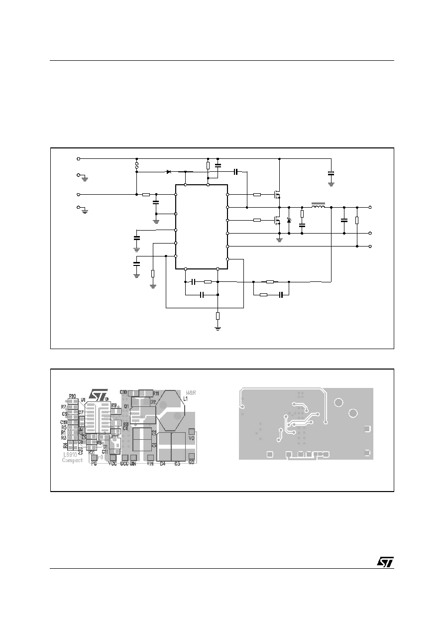
5A Demo Board Description
The demo board shows the operation of the device in a general purpose application. The interanl reference is
used for the regulation. The external power mosfets are included in one SO8 package to save space and in-
crease power density.The 12V input rail supplies the device while the power conversion starts from the 5V input
rail. The device is also able to operate with a single supply voltage; in this case the jumper J1on the board bot-
tom has to be closed and a 5V to 12V input can be directly connected to the V
IN
input.
Figure 14. 5A Demo Board Schematic
Figure 15. PCB and Components Layouts
Efficiency
Figure 16 shows the measured efficiency versus load current for different values of output voltage. The measure
was done at 5V and 12V input for different values of the output voltage (2.5V, 3.3V and 5V only when Vin=12V).
Output voltage has been changed modifying the value of R1 in the demo board as reported in the part list.
L1
R7
C1,C2
C7
C3, C4
Q1/2
Q1/1
13
14
10
11
3
1
U1
L6910
VIN (+5V)
VOUT
PWRGD
6
12
5
4
2
15
7
9
VCC
GND
VREF
SS
OSC
OCSET
UGATE
PHASE
LGATE
PGND
PGOOD
VFB
COMP
C19
R1
C9
C6
D1
GNDIN
GNDOUT
R2
C8
C5
R6
C18
8
R5
R3
R4
C20
EAREF
BOOT
R9
R8
R10
D2
C10
R11
GNDCC
J1
VCC (+12V)
Component Side
Solder Side

17/21
L6910A L6910
Figure 16. Demoboard efficiency with V
CC
= V
IN
= 5V (left), and with V
CC
= V
IN
= 12V (right).
Part List
Resistors
R1
560
375
220
1%; (Vout = 2.5V)
1%; (Vout = 3.3V)
1%; (Vout = 5V)
SMD 0805
R2
10K
SMD 0805
R3
1K
SMD 0805
R4
33
SMD 0805
R5
2.7K
SMD 0805
R6
10
SMD 0805
R7
680
SMD 0805
R8, R9
2.2
SMD 0805
Capacitors
C1,C2
10
µ
F
TOKIN C34Y5U1E106ZTE12
SMD 7343
C3, C4
100
µ
F ≠ 6.3V
POSCAP 6TPB100M
SMD 7343
C5,C6,C9
100nF
SMD 0805
C7, C8
1nF
SMD 0805
C18
1.5n
SMD 0805
C19
15n
SMD 0805
C20
47n
SMD 0805
Magnetics
L1
10µH
T50-52B Core, 12T
Transistors
Q1
STS7DNF30L
STMicroelectronics
SO8
Diodes
D1
1N4148
SOT23
D2
STPS125A
STMicroelectronics
SMA
Ics
U1
L6910
STMicroelectronics
SO16Narrow
85
86
87
88
89
90
91
92
93
94
95
0
1
2
3
4
5
Output Current [A]
Efficiency [%]
Vout=3.3V
Vout=2.5V
60
65
70
75
80
85
90
95
0
1
2
3
4
5
Output Current [A]
Efficiency [%]
Vout=2.5V
Vout=3.3V
Vout=5V
L6910A L6910
18/21
APPLICATION IDEA: BUCK-BOOST CONVERTER 3V TO 10V INPUT / 5V 2A OUTPUT
Figure 17. buck-boost converter 3V to 10V input / 5V 2A Output Circuit
L1
R7
C1,C2
C7
C3, C4
Q1/2
Q1/1
13
14
10
11
3
1
U1
L6910
VIN (+2.5V to +12V)
VOUT
PWRGD
6
12
5
4
2
15
7
9
VCC
GND
VREF
SS
OSC
OCSET
UGATE
PHASE
LGATE
PGND
PGOOD
VFB
COMP
C19
R1
C9
C6
D1
GNDIN
GNDOUT
R2
C8
C5
R6
C18
8
R5
R3
R4
C20
EAREF
BOOT
R9
R8
R10
D2
GNDCC
VCC (+12V)
Q2/1
Q2/2
D3

19/21
L6910A L6910
SO16 Narrow
DIM.
mm
inch
MIN.
TYP.
MAX.
MIN.
TYP.
MAX.
A
1.75
0.069
a1
0.1
0.25
0.004
0.009
a2
1.6
0.063
b
0.35
0.46
0.014
0.018
b1
0.19
0.25
0.007
0.010
C
0.5
0.020
c1
45∞ (typ.)
D (1)
9.8
10
0.386
0.394
E
5.8
6.2
0.228
0.244
e
1.27
0.050
e3
8.89
0.350
F (1)
3.8
4
0.150
0.157
G
4.6
5.3
0.181
0.209
L
0.4
1.27
0.016
0.050
M
0.62
0.024
S
(1) D and F do not include mold flash or protrusions. Mold flash or potrusions shall not exceed 0.15mm (.006inch).
OUTLINE AND
MECHANICAL DATA
8∞(max.)
0016020
Weight: 0.20gr

L6910A L6910
20/21
OUTLINE AND
MECHANICAL DATA
DIM.
mm
inch
MIN.
TYP.
MAX.
MIN.
TYP.
MAX.
A
1.2
0.047
A1
0.15
0.006
A2
0.8
1.0
1.05
0.031
0.039
0.041
b
0.19
0.3
0.007
0.012
c
0.09
0.2
0.003
0.008
D (*)
4.9
5.0
5.1
0.192
0.197
0.200
D1
1.7
0.067
E
6.2
6.4
6.6
0.244
0.252
0.260
E1 (*)
4.3
4.4
4.5
0.169
0.173
0.177
E2
1.5
0.059
e
0.65
0.026
L
0.45
0.6
0.75
0.018
0.024
0.029
L1
1.0
0.039
k
0∞ (min), 8∞ (max)
aaa
0.10
0.004
(*) Dimensions D and E1 does not include mold flash or
protusions. Mold flash or protusions shall not exeed
0.15mm per side.
HTSSOP16
7419276
(Exposed Pad)
3.0
3.0
0.118
0.118

Information furnished is believed to be accurate and reliable. However, STMicroelectronics assumes no responsibility for the consequences
of use of such information nor for any infringement of patents or other rights of third parties which may result from its use. No license is granted
by implication or otherwise under any patent or patent rights of STMicroelectronics. Specifications mentioned in this publication are subject
to change without notice. This publication supersedes and replaces all information previously supplied. STMicroelectronics products are not
authorized for use as critical components in life support devices or systems without express written approval of STMicroelectronics.
The ST logo is a registered trademark of STMicroelectronics
Æ
2003 STMicroelectronics - All Rights Reserved
STMicroelectronics GROUP OF COMPANIES
Australia - Brazil - Canada - China - Finland - France - Germany - Hong Kong - India - Israel - Italy - Japan -Malaysia - Malta - Morocco -
Singapore - Spain - Sweden - Switzerland - United Kingdom - United States.
http://www.st.com
21/21
L6910A L6910