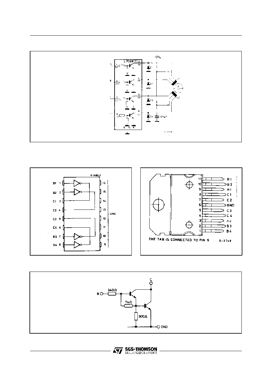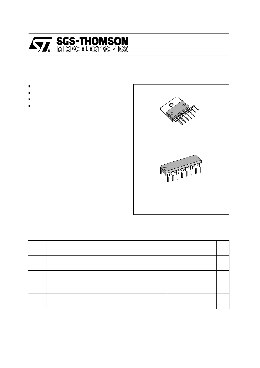
L702
2A QUAD DARLINGTON SWITCH
SUSTAINING VOLTAGE: 70 V
2 A OUTPUT
HIGH CURRENT GAIN
IDE AL FOR DRI VING SOLENOIDS, DC
MOTORS, STEPPER MOTORS, RELAYS,
DISPLAYS, ETC.
DESCRIPTION
The L702 is a monolithic integrated circuit for high
current and high voltage switching applications. It
comprises four darlington transistors with common
emitter and open collector suitable for current sink-
ing applications mounted on the new POWERDIP
and MultiwattÆ packages.
This circuit reduces components, sizes and costs;
it can provide direct interface between low level
logic and a variety of high current applications.
October 1991
Multiwatt-11
ORDER CODES : L702B - Powerdip
L702N - Multiwatt
Powerdip 8 + 8
Symbol
Parameter
Value
Unit
V
CEX
Collector-emitter Voltage (input open)
90
V
V
i
Input Voltage
30
V
I
C
Collector Current
3
A
P
tot
Total Power Dissipation at T
pin
9 to 16
90
∞
C
Powerdip
4
W
Total Power Dissipation at T
amb
70
∞
C
1.1
W
Total Power Dissipationa t T
case
90
∞
C
Multiwatt
20 W
T
stg
Storage Temperature
-55 to 150
∞
C
T
j
Operating Junction Temperature
-25 to 150
∞
C
ABSOLUTE MAXIMUM RATINGS
}
1/7

Symbol
Parameter
Value
Unit
R
th j-amb
Thermal Resistance Junction Ambient
Powerdip
Max
70
∞
C/W
R
th j-pins 9/16
Thermal Resistance Junction Pins 9 to 16
Max
14
∞
C/W
R
th j-case
Thermal Resistance Junction-case
Multiwatt
Max
3
∞
C/W
THERMAL DATA
}
Symbol
Parameter
Test conditions
Min.
Typ.
Max.
Unit
I
CEX
Output Leakage Current
V
CE
= 90 V
10
50
µ
A
V
CE(sust)
Collector Emitter (
∞
) Sustaining
Voltage
I
C
= 100 mA
70
V
V
CE(sat)
Collector Emitter Saturation
Voltage
I
C
= 1.25 A
I
i
= 2 mA
1.3
1.9
V
h
FE
DC Forward Current Gain
I
C
= 1 A
V
CE
= 3 V
1.000
4.000
I
i
Input Current
V
i
= 3.75 V
V
i
= 2.4 V
Open Collector
7
3
11
6
mA
mA
V
i
Input Voltage
Off Condition
V
CE
= 70 V
I
C
0.1 mA
0.4
V
On
Condition
V
CE
= 3 V
I
C
1 A
2.4
V
T
on
Turn On Time
V
s
= 12 V
0.3
µ
s
T
off
Turn Off Time
R
L
= 10
1
µ
s
ELECTRICAL CHARACTERISTICS (T
case
= 25
∞
C unless otherwise specified)
Figure 1. Switching Time.
Figure 2. t
on
and t
off
Test Circuit.
3/7
L702

Figure 3. Peak Collector Current
vs. Duty Cycle and Number of
Outputs (L702B only)
Fi g ure 4 . C ol l ect or E mi t t er
Saturation Voltage vs. Collector
Current.
Figure 5. Collector Current vs.
Input Voltage.
Figure 6. Input Current vs. Input
Voltage.
Figure 7. Safe Operating Areas
(L702B).
Figure 8. Safe Operating Areas
(L702N).
4/7
L702