1/34
November 2004
s
OUTPUT CURRENT TO 1.5A
s
OUTPUT VOLTAGES OF 5; 5.2; 6; 8; 8.5; 9;
10; 12; 15; 18; 24V
s
THERMAL OVERLOAD PROTECTION
s
SHORT CIRCUIT PROTECTION
s
OUTPUT TRANSITION SOA PROTECTION
DESCRIPTION
The L7800 series of three-terminal positive
regulators is available in TO-220, TO-220FP,
TO-220FM, TO-3 and D
2
PAK packages and
several fixed output voltages, making it useful in a
wide range of applications. These regulators can
provide local on-card regulation, eliminating the
distribution problems associated with single point
regulation. Each type employs internal current
limiting, thermal shut-down and safe area
protection, making it essentially indestructible. If
adequate heat sinking is provided, they can
deliver over 1A output current. Although designed
primarily as fixed voltage regulators, these
devices can be used with external components to
obtain adjustable voltage and currents.
L7800
SERIES
POSITIVE VOLTAGE REGULATORS
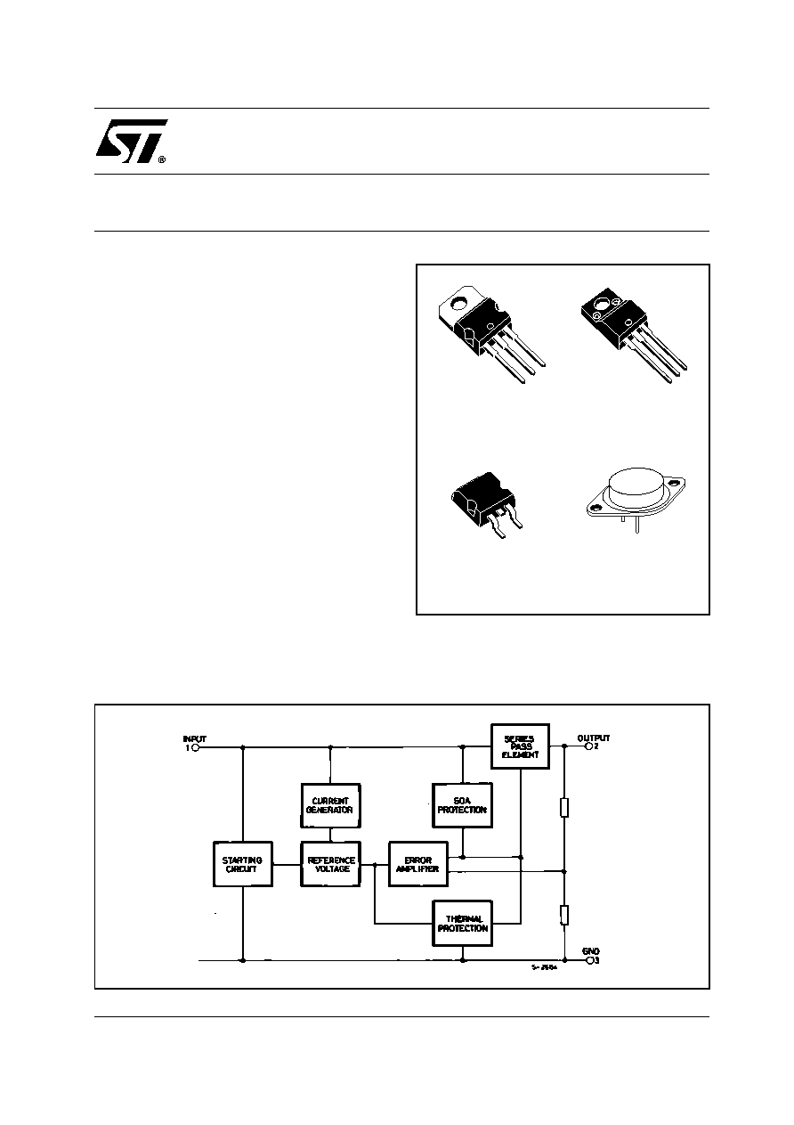
Figure 1: Schematic Diagram
TO-220
D
2
PAK
TO-3
TO-220FP
TO-220FM
Rev. 12
L7800 SERIES
2/34
Table 1: Absolute Maximum Ratings
Absolute Maximum Ratings are those values beyond which damage to the device may occur. Functional operation under these condition is
not implied.
Table 2: Thermal Data
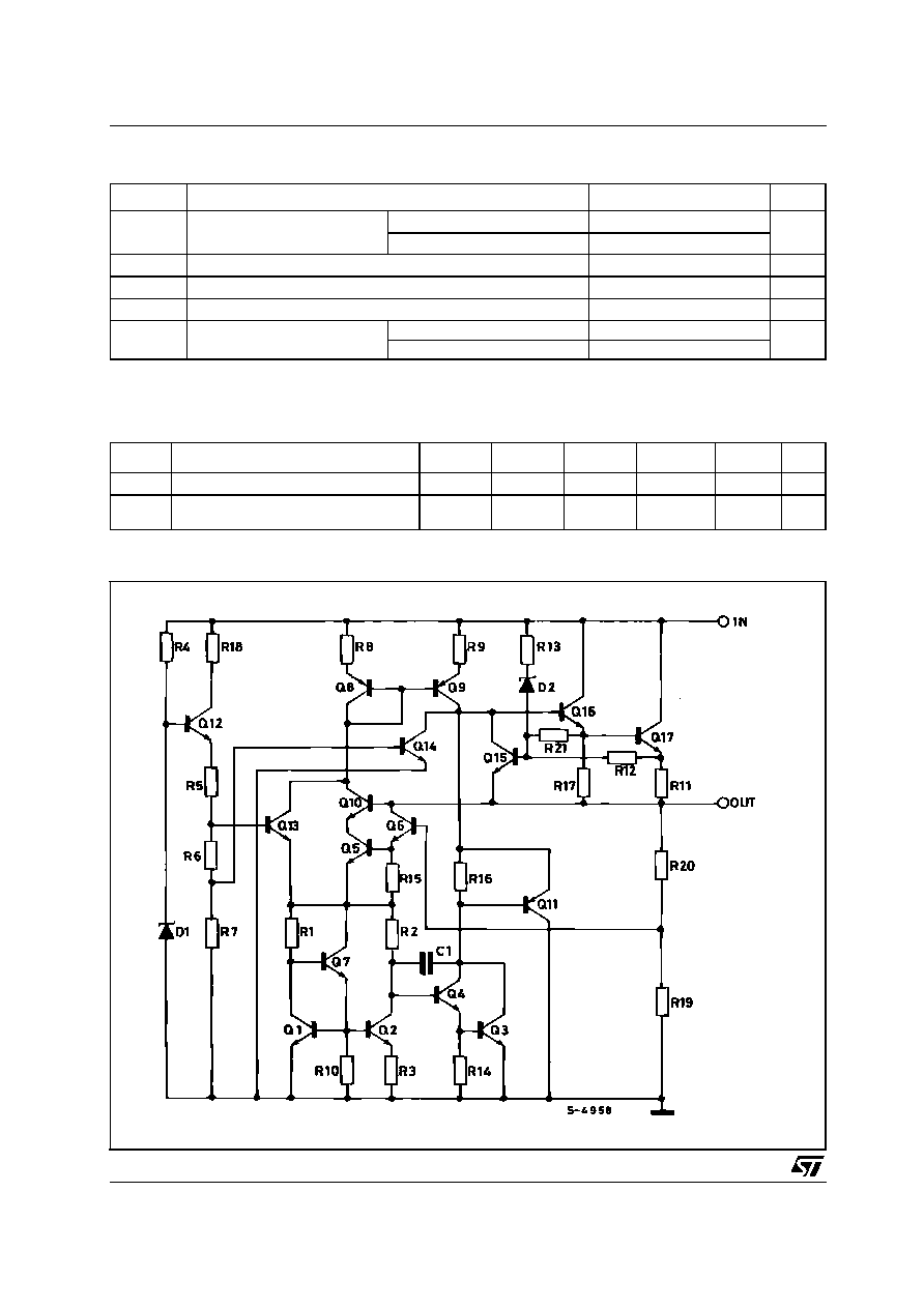
Figure 2: Schematic Diagram
Symbol
Parameter
Value
Unit
V
I
DC Input Voltage
for V
O
= 5 to 18V
35
V
for V
O
= 20, 24V
40
I
O
Output Current
Internally Limited
P
tot
Power Dissipation
Internally Limited
T
stg
Storage Temperature Range
-65 to 150
∞C
T
op
Operating Junction Temperature
Range
for L7800
-55 to 150
∞C
for L7800C
0 to 150
Symbol
Parameter
D
2
PAK
TO-220
TO-220FP TO-220FM
TO-3
Unit
R
thj-case
Thermal Resistance Junction-case Max
3
5
5
5
4
∞C/W
R
thj-amb
Thermal Resistance Junction-ambient
Max
62.5
50
60
60
35
∞C/W
L7800 SERIES
3/34
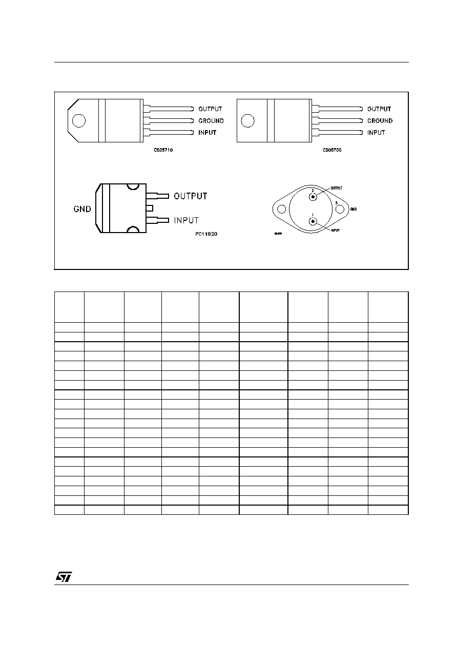
Figure 3: Connection Diagram (top view)
Table 3: Order Codes
(*) Available in Tape & Reel with the suffix "-TR".
TYPE
TO-220
(A Type)
TO-220
(C Type)
TO-220
(E Type)
D
2
PAK
(A Type) (*)
D
2
PAK
(C Type)
(T & R)
TO-220FP
TO-220FM
TO-3
L7805
L7805T
L7805C
L7805CV
L7805C-V
L7805CV1 L7805CD2T L7805C-D2TR
L7805CP
L7805CF
L7805CT
L7852C
L7852CV
L7852CD2T
L7852CP
L7852CF
L7852CT
L7806
L7806T
L7806C
L7806CV
L7806C-V
L7806CD2T
L7806CP
L7806CF
L7806CT
L7808
L7808T
L7808C
L7808CV
L7808C-V
L7808CD2T
L7808CP
L7808CF
L7808CT
L7885C
L7885CV
L7885CD2T
L7885CP
L7885CF
L7885CT
L7809C
L7809CV
L7809C-V
L7809CD2T
L7809CP
L7809CF
L7809CT
L7810C
L7810CV
L7810CD2T
L7810CP
L7812
L7812T
L7812C
L7812CV
L7812C-V
L7812CD2T
L7812CP
L7812CF
L7812CT
L7815
L7815T
L7815C
L7815CV
L7815C-V
L7815CD2T
L7815CP
L7815CF
L7815CT
L7818
L7818T
L7818C
L7818CV
L7818CD2T
L7818CP
L7818CF
L7818CT
L7820
L7820T
L7820C
L7820CV
L7820CD2T
L7820CP
L7820CF
L7820CT
L7824
L7824T
L7824C
L7824CV
L7824CD2T
L7824CP
L7824CF
L7824CT
TO-220 (Any Type)
TO-3
D
2
PAK (Any Type)
TO-220FP/TO-220FM
L7800 SERIES
5/34
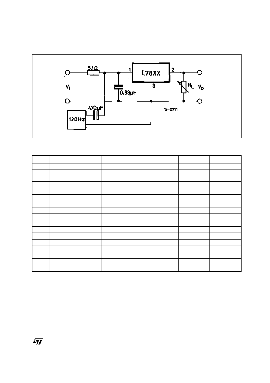
Figure 7: Ripple Rejection
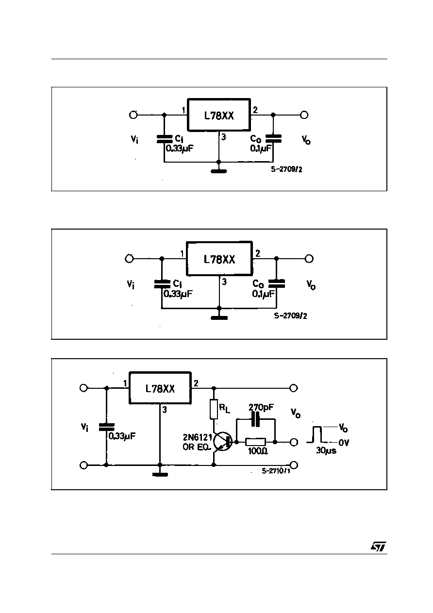
Table 4: Electrical Characteristics Of L7805 (refer to the test circuits, T
J
= -55 to 150∞C, V
I
= 10V,
I
O
= 500 mA, C
I
= 0.33 µF, C
O
= 0.1 µF unless otherwise specified).
(*) Load and line regulation are specified at constant junction temperature. Changes in V
O
due to heating effects must be taken into account
separately. Pulse testing with low duty cycle is used.
Symbol
Parameter
Test Conditions
Min.
Typ.
Max.
Unit
V
O
Output Voltage
T
J
= 25∞C
4.8
5
5.2
V
V
O
Output Voltage
I
O
= 5 mA to 1 A
P
O
15W
V
I
= 8 to 20 V
4.65
5
5.35
V
V
O
(*)
Line Regulation
V
I
= 7 to 25 V
T
J
= 25∞C
3
50
mV
V
I
= 8 to 12 V
T
J
= 25∞C
1
25
V
O
(*)
Load Regulation
I
O
= 5 mA to 1.5 A
T
J
= 25∞C
100
mV
I
O
= 250 to 750 mA
T
J
= 25∞C
25
I
d
Quiescent Current
T
J
= 25∞C
6
mA
I
d
Quiescent Current Change
I
O
= 5 mA to 1 A
0.5
mA
V
I
= 8 to 25 V
0.8
V
O
/
T Output Voltage Drift
I
O
= 5 mA
0.6
mV/∞C
eN
Output Noise Voltage
B =10Hz to 100KHz
T
J
= 25∞C
40
µ
V/V
O
SVR
Supply Voltage Rejection
V
I
= 8 to 18 V
f = 120Hz
68
dB
V
d
Dropout Voltage
I
O
= 1 A
T
J
= 25∞C
2
2.5
V
R
O
Output Resistance
f = 1 KHz
17
m
I
sc
Short Circuit Current
V
I
= 35 V
T
J
= 25∞C
0.75
1.2
A
I
scp
Short Circuit Peak Current
T
J
= 25∞C
1.3
2.2
3.3
A