 | –≠–ª–µ–∫—Ç—Ä–æ–Ω–Ω—ã–π –∫–æ–º–ø–æ–Ω–µ–Ω—Ç: L9230 | –°–∫–∞—á–∞—Ç—å:  PDF PDF  ZIP ZIP |

1/25
L9230
March 2003
This is preliminary information on a new product now in development or undergoing evaluation. Details are subject to change without notice.
s
OPERATING SUPPLY VOLTAGE 5V TO 28V
s
TYPICAL R
DSon
= 150 m
FOR EACH
OUTPUT TRANSISTOR (AT 25∞C)
s
CONTINOUS DC LOAD CURRENT 5A
(T
case
< 100 ∞C)
s
OUTPUT CURRENT LIMITATION AT TYP. 6A
s
SHORT CIRCUIT SHUT DOWN FOR OUTPUT
CURRENTS OVER 8A
s
LOGIC- INPUTS TTL/CMOS-COMPATIBLE
s
OPERATING-FREQUENCY UP TO 30 kHz
s
OVER TEMPERATURE PROTECTION
s
SHORT CIRCUIT PROTECTION
s
UNDERVOLTAGE DISABLE FUNCTION
s
DIAGNOSTIC BY SPI OR STATUS-FLAG
(CONFIGURABLE)
s
ENABLE AND DISABLE INPUT
s
SO20 POWER PACKAGE
DESCRIPTION
The L9230 is an SPI controlled H-Bridge, designed
for the control of DC and stepper motors in safety crit-
ical applications and under extreme environmental
conditions.
The H-Bridge is protected against over temperature
and short circuits and has an under voltage lockout
for all the supply voltages "V
S
" (Main DC power sup-
ply). All malfunctions cause the output stages to go
tristate.
The H-Bridge contains integrated free-wheel diodes.
In case of free-wheeling condition, the lowside tran-
sistor is switched on in parallel of its diode to reduce
the current injected into the substrate.
Switching in parallel is only allowed, if the voltage-
level of the according output-stage is below the
ground-level.In this case it must be ensured, that the
upper transistor is switched off.
PowerSO20
BARE-DIE
ORDERING NUMBERS:
L9230
L9230-DIE1
PRELIMINARY DATA
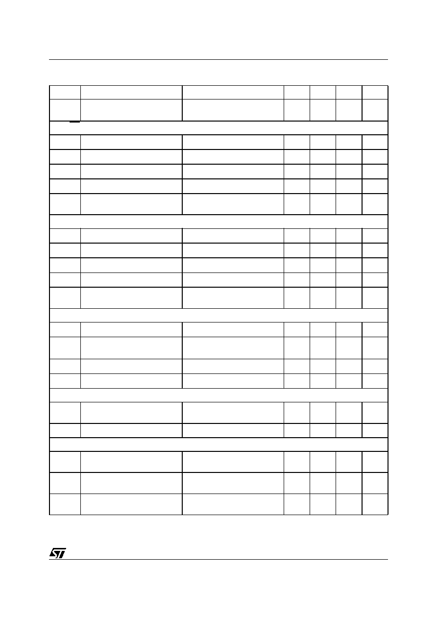
SPI CONTROLLED H-BRIDGE
BLOCK DIAGRAM
IN1
V
S
GND
OUT1
OUT2
IN2
DI
EN
DMS
SF/SCK
SS
SI
SO
LOGIC
UNDERVOLTAGE
V
S
INTERNAL 5V
SUPPLY
OVERCURRENT
HIGH-SIDE
OVERCURRENT
LOW-SIDE
GATE CONTROL
1
GATE CONTROL
2
OVER
TEMPERATURE
MAXIMUM
CURRENT
LIMITATION
D01AT470A
L9230
2/25
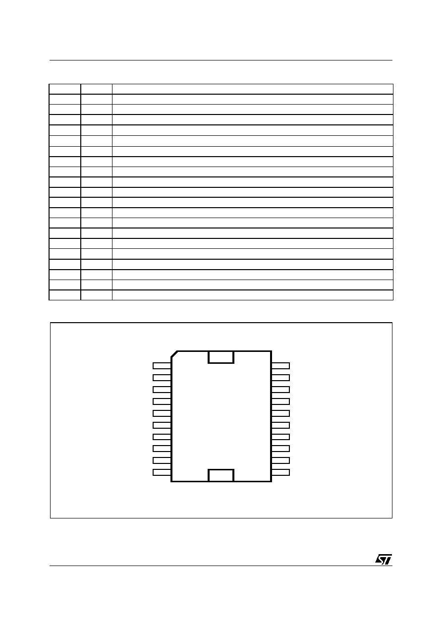
PIN FUNCTION
PIN CONNECTION (Top view)
N∞
Pin
Description
1 GND
Ground
2 SCK/SF
SPI-Clock/Status-flag
3 IN1
Input
1
4
V
S
Supply
voltage
5 V
S
Supply
voltage
6 OU1
Output
1
7
OU1
Output 1
8
SO
serial out
9 SI
serial
in
10
GND
Ground
11
GND Ground
12
DMS
Diagnostic-Mode selection (+ Supply Voltage for SPI-Interface)
13 EN
Enable
14 OU2
Output
2
15 OU2
Output
2
16 V
S
Supply
voltage
17 SS
Slave
select
18 DI
Disable
19 IN2
Input
2
20
GND
Ground
GND
SI
DMS
IN1
V
S
OU1
V
S
OU1
SO
SCK
GND
10
8
9
7
6
5
4
3
2
13
14
15
16
17
19
18
20
12
1
11
GND
D01AT471
EN
OU2
V
S
OU2
SS
DI
IN2
GND
3/25
L9230
ABSOLUTE MAXIMUM RATINGS
The integrated circuit must not be destroyed by use at the limit values.
Each limit value can be used, as long as no other limit is violated.
Voltage reference point:
All values are, if not otherwise stated, relative to ground.
Direction of current flow:
Current flow into a pin is positive.
Rise-, fall- and delaytimes:
If not otherwise stated, all rise times are between 10% and 90%, fall times
between 90% and 10% and delay times at 50% of the relevant steps.
THERMAL DATA
Symbol
Parameter
Test Condition
Min.
Typ.
Max.
Unit
V
S
Supply voltage
static destruction proof
-1
40
V
dynamic destruction proof t <0.5s
(single pulse, Tj < 85∞C)
-2
40
V
V
LI
Logic inputs
IN1, IN2, DI, EN, SS, SI, SCK,DMS
-0.5
7
V
I
LI
Logic inputs
IN1, IN2, DI, EN, SS, SI, SCK,DMS
-20
mA
V
LO
Logic outputs SF, SO
R
10k
-0.5
7
V
Symbol
Parameter
Test Condition
Min.
Typ.
Max.
Unit
T
j
Junction temperature
dynamic t < 1 s
-40
+150
+175
∞C
∞C
T
stg
Storage temperature
-55
+125
∞C
T
amb
Ambient temperature
-40
+125
∞C
R
th j-case
Thermal resistance junction to
case
(2)
3
∞C/W
T
j_sd
Thermal Shutdown Junction
Temperature Threshold
165
175
∞C
ELECTRICAL CHARACTERISTCS ( T
j
= -40 to +150∞C; V
S
= 5 to 28V)
Symbol
Parameter
Test Condition
Min.
Typ.
Max.
Unit
Power Supply
V
S
Supply Voltage
Static Condition
5
28
V
Dynamic Condition (t < 500ms)
40
V
Undervoltage Shutdown
(at least down to 2.5V)
(1)
4.7
5
V
Switch OFF voltage
4.5
5
V
Switch ON voltage
4.7
5
V
Hysteresis
200
mV
I
S
Supply current
f = 0 kHz, I
O
= 0 A
f = 20kHz, I
O
= 0 A
13
30
mA
mA
Note:
1. For supply voltages down to 2.5V the output stages are in tristate condition and the status flag is set to low. Below 2.5V the
device operates in undefined condition
2. Guaranteed by design and package characterization
L9230
4/25
Logic inputs
V
I
Logic Input Voltage
IN1, IN2, DI, EN
1
1.5
2
V
I
I
Logic Input Current
IN1, IN2, DI
V
I
1V
-200
-125
µ
A
I
EN
Input Current EN
V
IEN
2V
75
100
µ
A
t
dt
Detection Time EN, DI
3
4
µ
s
Power Outputs (OUT1, OUT2)
R
S
Switch on Resistance LS
R
OUT-Vs
, V
S
> 5 V
150
250
m
Switch on Resistance HS
R
OUT-GND,
V
S
> 5 V
150
250
m
Current Limitation
Peak value controlled
inductive load L = 0,8 to 5 mH
resistive load R = 0,8 to 1.8
|I
OU
|
max
|I
OU
|
max
Switch-off Current
-40 ∞C < T
j
< 165 ∞C
T
j
< 175 ∞C
5.5
6
2.5
7.7
A
A
t
a
Switch-off time
(2)
12
17
22
µ
s
t
b
Blanking time
(2)
8
11.5
15
µ
s
t
a
/t
b
Tracking
(2)
1.4
1.5
1.6
|I
OUK
|
Short circuit detection current
(1)
see figure 1
5.5
11
A
|I
OUK
|
Short Circuit Current Trecking
(1)
1600
mA
t
Reactivation time after internal
shut down
(2)
Overcurrent- or overtemperature
shut down to reactivation of the
output stage
1
ms
I
L
Leakage Current
Output stage switched off
1
mA
V
FD
Free-wheel diode forward voltage
I
O
= 3A, V
S
= 0V
2
V
t
rr
Free-wheel diode reverse
recovery time
(2)
100
ns
V
SFHigh
Output,,high" (SF not set)
(*)
V
S
= 5V, R
Pull_up
= 27K
4.1
V
|I
ou
|
max
Switch OFF Current
Tj = -40 to 165∞C
6
A
Tj = < 175∞C
2.5
A
I
SF
Output,,high" (SF not set)
(2)
V
SF
= 5V
20
µ
A
I
SF
Output,,low" (SF set)
(3 )
V
SF
= 1V
300
µ
A
V
SF
= 0.5V
100
µ
A
V
SF
= 0.8V
500
µ
A
ELECTRICAL CHARACTERISTCS ( T
j
= -40 to +150∞C; V
S
= 5 to 28V) (continued)
Symbol
Parameter
Test Condition
Min.
Typ.
Max.
Unit

5/25
L9230
(*) For lower pull up resistances than 27k
the specified value of xxxV (minimum) is guaranteed by design
Note: 1. In case of SC OUTx to Vs the switch off current is always higher than the start value of current regulation (
|I
OUK
| = |I
OUK
| - |I
OUmax
|
2. Guaranteed by design
3. Value is tested down to 6V. For supply voltage below 6V on increased current can be fed back in the device via a protection path
Timing
f
PWM Frequency
min. operating time 10
µ
s
2
30
kHz
f
S
Switching Frequency during
current limitation
5
30
kHz
t
don
Output ON-delay
IN1 --> OUT1 or IN2 --> OUT2
3
5
µ
s
t
doff
Output OFF-delay
3
5
µ
s
t
r
, t
f
Output rise-, fall Time
OUT1H--> OUT1L, OUT2H--> OUT2L,
IOUT = 3 A
OUT1L--> OUT1H, OUT2L--> OUT2H
0.2
0.4
1
µ
s
t
ddis
Disable Delay Time
DIn --> OUTn, En --> OUTn
3
4
µ
s
t
dp
Power on Delay Time
V
S
= on --> output stage active
15
ms
Delay time for fault detection
5
15
µ
s
|
I|
Effect of reverse current at power
supply
4,5V < V
DMS
< 5,5V
- I
Vs
< 3A
I for I
SI
, I
SO
, I
SS
, I
SCK
, I
IN1
, I
IN2
, I
EN
,I
DI
100
µ
A
ELECTRICAL CHARACTERISTCS ( T
j
= -40 to +150∞C; V
S
= 5 to 28V) (continued)
Symbol
Parameter
Test Condition
Min.
Typ.
Max.
Unit
L9230
6/25
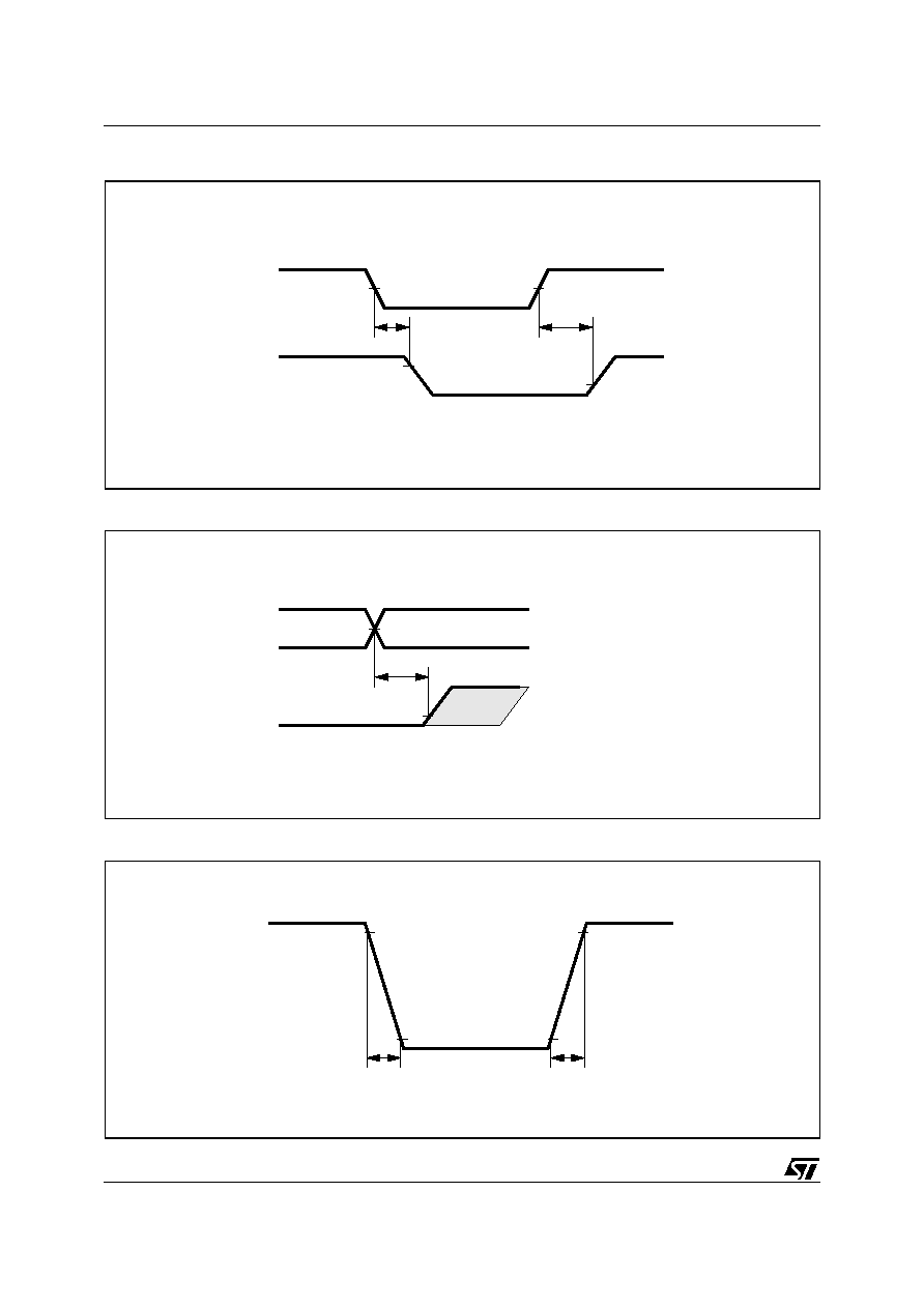
Figure 1. Output delay time
Figure 2. Disable delay time
Figure 3. Output switching time
50%
10%
90%
50%
t
don
t
doff
IN
n
OUT
n
D01AT472
50%
10%
Z
t
ddis
DI
n
OUT
n
D01AT473
10%
90%
90%
t
f
t
r
OUT
n
D01AT474

7/25
L9230
Figure 4.
Figure 5.
typ 6.6A
6.6A
>8A
CURRENT LIMITATION
OVERCURRENT
LOAD
CURRENT
DETAIL A
OVERCURRENT
DETECTION
ta = SWITCH_OFF TIME IN CURRENT LIMITATION
tb = CURRENT LIMITATION BLANKING TIME
ta
tb
CONTROL
SIGNAL
A
STATUS
FLAG
D01AT475
Range of
Overtemperature
switch-off
Tj
Tolerance-range
of temperature-dependent
current-reduction
165∞C
6.6A
2.5A
Imax
175∞C
Temperature-depending current-limitation
Maximum rating for junction temperature
for < 1s 175∞C
Overtemperature switch-off
> 175∞C
Switch-off current in case of current limitation
6,6A ± 1,1A Tj < 165∞C
For 165∞C < Tj < 175∞C the maximum current decreases from
Imax. = 6,6A ± 1,1A to Imax. = 2,5A ± 1,1A.

L9230
8/25
SPI INTERFACE
The timing of L9230 is defined as follows:
- The change at output (SO) is forced by the rising edge of the SCK signal.
- The input signal (SI) is taken over on the falling edge of the SCK signal.
- SS = active without any clocks at SCK is not allowed
- The data received during a writing access is taken over into the internal registers on the rising edge of the SS
signal, if exactly 16 SPI clocks have been counted during SS = active.
Figure 6.
ELECTRICAL CHARACTERISTCS ( continued)
Symbol
Parameter
Test Condition
Min.
Typ.
Max.
Unit
Input SCK (SPI clock input 4.5V < DMS < 5.5V)
V
SCKL
Low Level
1
V
V
SCKH
High Level
2
V
V
SCK
Hysteresis
0.1
0.4
V
C
SCK
Input Capacity
10
pF
SO
SI
MSB IN
Bit (n-4)...1
LSB IN
Bit (n-4)...1
1
4
5
6
SCK
SS
7
8
n = 16
9
10
3
2
Bit (n-3)
Bit 0; LSB
tristate
Bit (n-3)
Bit (n-2)
11
12
ELECTRICAL CHARACTERISTICS (continued)
9/25
L9230
-I
SCK
Input Current
Pull up current source connected
to V
S
20
50
µ
A
Input SS
(Slave select signal)
V
SSL
Low Level
L9230 is selected
1
V
V
SSH
High Level
2
V
V
SS
Hysteresis
0.1
0.4
V
C
SS
Input Capacity
10
pF
-I
SS
Input Current
Pull up current source connected
to VDD
20
50
µ
A
Input SI
(SPI data input)
V
SIL
Low Level
1
V
V
SIH
High Level
2
V
V
SI
Hysteresis
0.1
0.4
V
C
SI
Input Capacity
10
pF
-I
SI
Input Current
Pull up current source connected
to VDD
20
50
µ
A
Output SO
(Tristate output of the L9230 (SPI output); On active reset (DI) output SO is in tristate.)
V
SOL
Low Level
I
SO
= 2mA
0.4
V
V
SOH
High Level
I
SO
= -2mA
V
VDD
- 0.75
V
C
SO
Capacity
Capacity of the pin in tristate
10
pF
I
SO
Leakage Current
In tristate
-10
10
µ
A
Input DMS
(Supply-Input for the SPI-Inteface and Selection Pin for SPI- or SF-Mode)
V
i
Input Voltage
SPI-Mode
Status-Flag-Mode
3.5
0.8
V
V
I
c
Input Current
SPI-Mode
10
mA
Timing
t
cyc
Cycle-Time
(referred to master)
200
ns
t
lead
Enable Lead Time
(referred to master)
100
ns
t
lag
Enable Lag Time
(referred to master)
150
ns
Symbol
Parameter
Test Condition
Min.
Typ.
Max.
Unit
ELECTRICAL CHARACTERISTICS (continued)

L9230
10/25
t
v
Data Valid CL = 40pF
Data Valid CL = 200pF
(referred to L9230)
40
150
ns
ns
t
su
Data Setup Time
(referred to master)
50
ns
t
h
Data Hold Time
(referred to master)
20
ns
t
dis
Disable Time
(referred to L9230)
100
ns
t
dt
Transfer Delay
(referred to master)
150
ns
t
SCKH
Serial clock high time
(referred to master)
50
µ
s
t
SCKL
Access time
(referred to master)
8.35
ns
Clock inactive before
chipselect becomes valid
200
ns
Clock inactive after
chipselect becomes valid
200
ns
t
rs
rise-, fall time
Load on SO 50pF
20
ns
DIAGNOSTIC
Diagnostic Threshold
(Open Load Detection DMS > 4,5V, EN < 0,8V)
V
OUT1
V
OUT2
Load is available
0.8
0.8
V
V
V
OUT1
V
OUT2
Load is missing
1
V
S
0.8
V
V
I
OUT2
-I
OUT1
Diagnostic Current
DMS > 4.5V, EN < 0.8V
DMS > 4.5V, EN < 0.8V
700
1000
1000
1500
1300
2000
µ
A
µ
A
Tracking Diagnostic Current
I
OUT1
/ I
OUT2
1.4
1.5
1.6
t
D
Delay Time
30
100
ms
Symbol
Parameter
Test Condition
Min.
Typ.
Max.
Unit

11/25
L9230
TRUTH TABLE
1.)
In case of undervoltage tristate and status-flag are reset automatically.
2.)
Whenever overcurrent or overtemperature is detected, the fault is stored (i.e. status-flag remains low).
The tristate conditions and the status-flag
3)
are reset via DI or EN.
L
=
Low
H
=
High
X = High or Low
Z = High impedance
(all output stage transistors are switched off in static state. For more inform. see next page )
Overcurrent:
I
OUT1,2
>8,0 A
Overtemperature:
T
j
>175
∞
C
Undervoltage:
V
Vs-GND
<5.0 V (at least down to 2,5V)
3.)
If Mode ,,Status-Flag" is selected (see 1.5)
4.) If Mode ,,SPI-Diagnosis is selected (see 1.5)
Pos.
DI
EN
IN1
IN2
OUT1
OUT2
SF
3)
SPI
4)
DIA_REG
1. forward
L
H
H
L
H
L
H
See
Page
17
2. reverse
L
H
L
H
L
H
H
3. Free-wheeling low
L
H
L
L
L
L
H
4. Free-wheeling high
L
H
H
H
H
H
H
5. Disable
H
X
X
X
Z
Z
L
6. Enable
X
L
X
X
Z
Z
L
7. IN1 disconnected
L
H
Z
X
H
X
H
8. IN2 disconnected
L
H
X
Z
X
H
H
9. DI disconnected
Z
X
X
X
Z
Z
L
10. EN disconnected
X
Z
X
X
Z
Z
L
11. Current limit. active
L
H
X
X
Z
Z
H
12. Undervoltage
1.)
X
X
X
X
Z
Z
L
13. Overtemperature
2.)
X
X
X
X
Z
Z
L
14. Overcurrent
2.)
X
X
X
X
Z
Z
L

L9230
12/25
Description of the state ,,Z"
The state ,,Z" has, depending on the previous operating condition different meaning.
1. dynamical
I. e. the inductive load is current carrying and is switched off according to Pos. 5, 6, 9, 10, 11, 12, 13, or
14 of the truth table
a.) All output stage transistors are switched off.
b.) The current flow is continued via the free wheeling diodes.
c.) Free wheeling is detected by a negative voltage-level at OUn.
d.) Switch on of the parallel-transistor of the current carrying diode.
f.) Free wheeling is finshed, if the voltage-level on OUn is positive again.
2. statical
g.) all output-stages switched off.
Figure 7.
Z∫
CURRENT
CARRYNG
I
VS
-I
GND
V
S
-
V
S
-VD
S
-V
S
I
LOAD
V
OUn
FREE WHEELING
HIGH IMPEDANCE
D01AT478
Z

13/25
L9230
DIAGNOSTIC
The Diagnosis-Mode can be selected between SPI-Diagnosis and Status-Flag Diagnosis.
The choise of the Diagnosis-Mode is selected by the voltage-level on pin 12 (DMS Diagnosis Mode Selection).
DMS = GND Status-Flag
DMS = Vcc SPI-Diagnostic
For the connection of pins SI, SO, SS and SCK/SF see Fig. 10 respectively Fig. 11.
Status-Flag
The Status-Flag showes the condition ,,tristate".
At the following fault-cases the output-stages switches in tristate and set the status-flag from high to low.
- Short circuit of OUT1 or OUT2 against V
S
or GND
- Short circuit between OUT1 and OUT2
- Overcurrent
- Overtemperature
- Undervoltage on V
S
In cause of short circuit or overcurrent, the fault will be stored.
The output stage switches in tristate and the status-flag is set from high level to low-level if the specified value
is exceeded.
If the voltage level changes from high to low on DI or from low to high on EN, the output stage switches on again
and the status-flag is reset to high-level.
In cause of overtemperature the fault will be stored.
The output stage switches in tristate and the status-flag is set from high level to low-level if the specified value
is exceeded.
the voltage level changes from high to low on DI or from low to high on EN, the output stage switches on again
and the status-flag is reset to high-level.
In cause of undervoltage on V
Batt
the output stage switches in tristate and the status-flag is set from high level
to low-level if the specified value is fallen. If the voltage has risen about the specified value again, the output
stage switches on again and the status-flag is reset to high-level.
The maximum current which can flow under normal operating conditions is limited to typical I
max.
= 6,6A .
When the maximum current value is reached, the output stages are switched tristate for a fixed time.
According to the time-constant the current decreases exponentially until the next switch-on occurs.
At the end if the fixed time the output stage switches on again and the status-flag is reset to high-level.
L9230
14/25
SPI-INTERFACE
General Discription
The serial SPI interface establishes a communication link between L9230 and the systems microcontroller.
L9230 always operates in slave mode whereas the controller provides the master function.
The maximum baud rate is 2 MBaud (200pF).
Applying an active slave select signal at SS L9230 is selected by the SPI master. SI is the data input (Slave In),
SO the data output (Slave Out). Via SCK (Serial Clock Input) the SPI clock is provided by the master.
In case of inactive slave select signal (High) the data output SO goes into tristate.
Figure 8.
Depending on the application the first two bits of an instruction may be used to estabish an extended
device-addressing. This gives the opportunity to operate up to 4 Slave-devices sharing one common SS signal
from the Master-Unit
Power Supply of the SPI-Interface
SPI-Logic and I/O-Pins are alternativ supplied from DMS or Vcc internal, depending on which voltage is higher.
That is why diagnosis of the EN-/DI-Pins is always possible, even in case of missing H-Bridge-power supply e.g.
during ,,Vorlauf/Nauchlauf".
SPI Control:
SI
SS
State Machine
Shift Register
Clock Counter
Control Bits
Parity Generator
DMS
SPI Power Supply
DIA_REG

15/25
L9230
Characteristics of the SPI Interface
1)
When DMS is > 3,5V, the SPI is active, independent of the state of EN or DI and the voltage on V
S
.
During active reset conditions (DMS < 3,5V) the SPI is driven into its default state.
When reset becomes inactive, the state machine enters into a waitstate for the next instruction.
2)
If the slave select signal at SS is inactive (high), the state machine is forced to enter the
waitstate, i.e. the state machine waits for the following instruction.
3)
During active (low) state of the select signal SS the falling edge of the serial clock signal
SCK will be used to latch the input data at SI. Output data at SO are driven with the rising
edge of SCK. Further processing of the data according to the instruction ( i.e. modification
of internal registers) will be triggered by the rising edge of the SS signal. (-> See Note)
3 ) Chipaddress:
In order to establish the option of extended addressing the uppermost two bits of the
instruction-byte ( i.e the first two SI-bits of a Frame ) are reserved to send a chipaddress.
To avoid a busconflict the output SO must stay high impedant during the addressing
phase of a frame (i.e. until the addressbits are recognised as valid chipaddress).
This tristate behavior should be realised in any case, regardless wether the extended
addressoption is used or not.
If the chipaddress does not match, the according access will be ignored and SO remains high
impedant for the complete frame regardless which frametype is applied.
5)
Check byte:
Simultaneously to the receipt of an SPI instruction L9230 transmitts a check byte via the
output SO to the controller. This byte indicates regular or irregular operation of the SPI.
It contains an initial bitpattern and a flag indicating an invalid instruction of the previous access.
6)
On the read access the databits at the SPI input SI are rejected.
7)
Invalid instruction/access:
An instruction is invalid, if one of the following conditions is fulfilled:
- an unused instruction code is detected (see tables with SPI instructions).
- in case the previous transmission is not completed in terms of internal data processing.
( Violation of the minimum Access-Time. )
If an invalid instruction is detected, any modifications on registers of L9230 are not allowed.
In case an unused instruction code occured the databyte "ff
hex
" will be transmitted after
having sent the check byte.
In addition any access is invalid if the number of SPI clock pulses (falling edge) counted
during active SS differs from exactly 16 clock pulses (-> See Note).

L9230
16/25
SPI Communication
Figure 9. Reading access / 8 bit
SPI Instruction
The uppermost 2 bit of the instruction byte contains the chipadress. The individual chipadress is a mask-option
and must be defined in accordance to the SPI-Members sharing on SS line.
SPI Instruction-Format
SPI Instruction-Bytes
MSB
7
6
5
4
3
2
1
0
0
0
INSTR4
INSTR3
INSTR2
INSTR1
INSR0
INSW
Bit
Name
Description
7,6
CPAD1,0
Chip Adress (has to be `0', `0')
5-1
INSTR (4-0)
SPI instruction (encoding)
0
INSW
Don`t care
SPI Instruction
Encoding
Description
bit 7,6
CPAD1,0
bit 5,4,3,2,1
INSTR(4...0)
Bit 0
RD_IDENT
00
00000
0
read identifier
RD_VERSION
00
00001
1
read version
RD_DIA
00
00100
1
read DIA_REG
all others
no function
SPI INSTRUCTION
MSB
XXXX XXXX
SS
SI
VERIFICATION BYTE
MSB
DATA/8 BIT
MSB
SO
D01AT480
17/25
L9230
Reset of the Diagnostic Register DIA_REG
On the following conditions DIA_REG is reset:
- DI high
- EN low
- With the rising edge of the SS-signal after the SPI-Instruction RD_DIA.
- When the voltage on DMS exceeds the threshold for detecting SPI-Mode.
(after undervoltage condition)
- Undervoltage on V
S
(< 5,0V) sets Bit 0 .... Bit 3 of DIA_REG to 0000.
- If UB rises over about the undervoltage level, the Bits of DIA_REG are restored
(when V
S
internal or DMS > 3,5V)
Verification byte:
MSB
7
6
5
4
3
2
1
0
Z
Z
1
0
1
0
1
TRANS_F
Bit
Name
Description
0
TRANS_F
Bit = 1: error detected during previous transfer
Bit = 0: previous transfer was recognised as valid
1
Fixed to High
2
Fixed to Low
3
Fixed to High
4
Fixed to Low
5
Fixed to High
6
send as high impedance
7
send as high impedance

L9230
18/25
Diagnostics/Encoding of Failures
Description of the SPI Registers (SPI Instructions: RD_DIA)
Description of DIA_REG Bit7
Register: DIA_REG
7
6
5
4
3
2
1
0
DI
OT
CurrRed
CurrLim
DIA21
DIA20
Dia11
DIA10
State of Reset: FFH
Access by Controller: Read only
Bit
Name
Description
0
DIA 10
Diagnosis-Bit1 of OUT1
1
DIA 11
Diagnosis-Bit2 of OUT1
2
DIA 20
Diagnosis-Bit1 of OUT2
3
DIA 21
Diagnosis-Bit2 of OUT2
4
CurrLim
is set to ,,0" in case of current limitation
5
CurrRed
is set to ,,0" in case of temperature dependet current limitation
6
OT
is set to ,,0" in case of overtemperature
7
DI
shows the wired-or state of the Pins EN and DI
Encoding of the Diagnostic Bits of the Output-Stages OUT1 and OUT2
DIA21
DIA20
DIA11
DIA10
-
-
0
0
Short circuit over load (SCOL)
-
-
0
1
Short circuit to battery on OUT1 (SCB1)
-
-
1
0
Short circuit to ground on OUT1 (SCG1)
-
-
1
1
No error detected on OUT1
0
0
-
-
Open load (OL)
0
1
-
-
Short circuit to battery on OUT2 (SCB2)
1
0
-
-
Short circuit to ground on OUT2 (SCG2)
1
1
-
-
No error detected on OUT2
0
0
0
0
Undervoltage on Pin UB
EN
DI
DIA_REG Bit7
0
0
0
0
1
0
1
0
1
1
1
0

19/25
L9230
Device Identifier
The IC`s identifier is used for production test purposes and features plug & play functionality depending on the
systems software release. It is made up on a device-number and a revision number each one read-only acces-
sible via standardised instructions.
The Device number is defines once to allow indentification of different IC-Types by software.
The Revision number may be utilised to distinguish different states of hardware. The contents is divided into an
upper 4 bit field reserved to define revisions correspondending to specific software releases.
The lower 4 bit field is utilised to indentify the actual maskset.
Both (SWR and MSR) will start with 0000
b
and are increased by 1 every time an according modification of the
hardware is introduced.
Reading the IC Identifier (SPI Instruction: RD_IDENT):
Reading the IC revision number (SPI Instruction: RD_VERSION):
IC Identifier1 (Device ID)
7
6
5
4
3
2
1
0
ID7
ID6
ID5
ID4
ID3
ID2
ID1
ID0
Bit
Name
Description
7...0
ID(7...0)
ID-No.: 10100001
L9230
IC's revision number
7
6
5
4
3
2
1
0
SWR3
SWR2
SWR1
SWR0
MSR3
MSR2
MSR1
MSR0
Bit
Name
Description
7...4
SWR(3...0)
Revision corresponding to Software release: 0Hex
3...0
MSR(3...0)
Revision corresponding to Maskset: 0Hex

L9230
20/25
Figure 10. Application example with SPI-Interface
Figure 11. Application example with Status-Flag
µ
C
VOLTAGE
REGULATOR
POWER-ON
RESET
IN1
DMS
GND
D01AT481
UB
V
CC
V
BATT
RESET
IN2
DI
SCK
SS
SO
SI
EN
I.E. WATCH
DOG
µ
P
M
OUT1
OUT2
µ
C
VOLTAGE
REGULATOR
POWER-ON
RESET
IN1
DMS
47K
GND
D01AT482
UB
V
CC
V
BATT
RESET
IN2
DI
SF
SS
SO
SI
EN
I.E. WATCH
DOG
µ
P
M
OUT1
OUT2
21/25
L9230
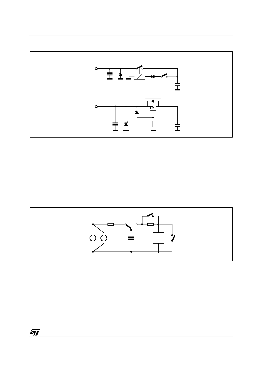
Figure 12. Application examples for Overvoltage- and Reverse-Voltage Protection
ESD-SOLIDITY
The connection pins of the IC have to be protected against Electrostatic Discharge ESD) by suitable integrated
protection structures.
The integrated circuit has to meet the demand of the ,,Human-Body-Model" with V
C
= ± 4kV
C = 100pF and R2 = 1,5k
(330
for OUT1 and OUT2).
Thereby any defect or destruction of the integrated circuit must not occur.
The protection structures realized to reach the ESD-strength have to be coordinated.
The ESD-strength has to be verified by the test circuit given as below.
Figure 13.
For the Pins 4, 5, 6, 7, 14 and 15
U
C
= + 4kV
R
1
= 100k
R
2
= 330
C = 100pF
Number of pulses each pin: 18
Frequency: 1Hz
Arrangement and performance:
The requirements of MIL883D Methode 3015 have to be fulfilled.
H-BRIDGE
H-BRIDGE
Version 1 REVERSE POLARITY PROTECTION VIA MAIN RELAIS
Version 2 REVERSE POLARITY PROTECTION VIA ACTIVE DIODE
MAIN
RELAIS
IGNITION
SWITCH
BATTERY
BATTERY
V
S
V
S
V
S
< 40V
V
S
< 40V
D01AT483
=
V
R1
R2
S2
S1
C
OUT
U
S
S3
(1)
DC-
VOLTMETER
(2)
D01AT484

L9230
22/25
ISO-PULSES
In the main-power-supply-system disturbance transients according to ISO 7637-1 First Edition 1990-06-01
may occur.
By means of external components (see Fig. 12) the following maximum ratings of the IC will not be exceeded.
statical
-1V ...... +40V
dynamical for t < 500 ms
-2V ...... +40V
APPENDIX A
Figure 14.
OUT1
OUT2
Load available
1
1
Open Load
1
0
SC -> GND on OUT1 with Load
0
0
SC detected on normal operation
SC -> GND on OUT2 with Load
0
0
SC detected on normal operation
SC -> UB on OUT1 with Load
1
1
SC detected on normal operation
SC -> UB on OUT2 with Load
1
1
SC detected on normal operation
SC -> GND on OUT1 Open Load
0
0
OL not detected Double Fault
SC -> GND on OUT2 Open Load
1
0
OL detected
SC -> UB on OUT1 Open Load
1
0
OL detected
SC -> UB on OUT2 Open Load
1
1
OL not detected Double Fault
1.5 mA
1 mA
OUT1
OUT2
IN2
IN1
VBatt
int 5V

23/25
L9230
APPENDIX B
Figure 15. Voltage Supply of SPI-Logic and EN/DI-Logic
SPI-
Logic
EN/DI-
Logic
Undervoltage
on VBatt
DMS
SO
SI
SCK
SS
EN
DI
VBatt
DMS = GND EN/DI-Logic is supplied from internal VCC
DMS = VCC EN/DI-Logic is supplied from DMS (OR int. VCC)
Output-
Stage
Failure and Status
Output Stage
Status
EN/DI
internal
Vcc

L9230
24/25
OUTLINE AND
MECHANICAL DATA
e
a2
A
E
a1
PSO20MEC
DETAIL A
T
D
1
10
11
20
E1
E2
h x 45
DETAIL A
lead
slug
a3
S
Gage Plane
0.35
L
DETAIL B
R
DETAIL B
(COPLANARITY)
G
C
- C -
SEATING PLANE
e3
b
c
N
N
H
BOTTOM VIEW
E3
D1
DIM.
mm
inch
MIN.
TYP.
MAX.
MIN.
TYP.
MAX.
A
3.6
0.142
a1
0.1
0.3
0.004
0.012
a2
3.3
0.130
a3
0
0.1
0.000
0.004
b
0.4
0.53
0.016
0.021
c
0.23
0.32
0.009
0.013
D (1)
15.8
16
0.622
0.630
D1
9.4
9.8
0.370
0.386
E
13.9
14.5
0.547
0.570
e
1.27
0.050
e3
11.43
0.450
E1 (1)
10.9
11.1
0.429
0.437
E2
2.9
0.114
E3
5.8
6.2
0.228
0.244
G
0
0.1
0.000
0.004
H
15.5
15.9
0.610
0.626
h
1.1
0.043
L
0.8
1.1
0.031
0.043
N
8∞ (typ.)
S
8∞ (max.)
T
10
0.394
(1) "D and E1" do not include mold flash or protusions.
- Mold flash or protusions shall not exceed 0.15mm (0.006")
- Critical dimensions: "E", "G" and "a3".
PowerSO20
0056635
JEDEC MO-166
Weight:
1.9gr

Information furnished is believed to be accurate and reliable. However, STMicroelectronics assumes no responsibility for the consequences
of use of such information nor for any infringement of patents or other rights of third parties which may result from its use. No license is granted
by implication or otherwise under any patent or patent rights of STMicroelectronics. Specifications mentioned in this publication are subject
to change without notice. This publication supersedes and replaces all information previously supplied. STMicroelectronics products are not
authorized for use as critical components in life support devices or systems without express written approval of STMicroelectronics.
The ST logo is a registered trademark of STMicroelectronics
Æ
2003 STMicroelectronics - All Rights Reserved
STMicroelectronics GROUP OF COMPANIES
Australia - Brazil - Canada - China - Finland - France - Germany - Hong Kong - India - Israel - Italy - Japan -Malaysia - Malta - Morocco -
Singapore - Spain - Sweden - Switzerland - United Kingdom - United States.
http://www.st.com
25/25
L9230