 | –≠–ª–µ–∫—Ç—Ä–æ–Ω–Ω—ã–π –∫–æ–º–ø–æ–Ω–µ–Ω—Ç: L9341V | –°–∫–∞—á–∞—Ç—å:  PDF PDF  ZIP ZIP |
L9341
QUAD LOW SIDE DRIVER
AVANCE DATA
DU/DT AND DI/DT CONTROL
PWM CONTROLLED OUTPUT CURRENT
SHORT CURRENT PROTECTION AND DI-
AGNOSTIC
INTEGRATED FLYBACK DIODE
UNDERVOLTAGE SHUTDOWN
OVERVOLTAGE AND UNDERVOLTAGE DI-
AGNOSTIC
OVERTEMPERATURE DIAGNOSTIC
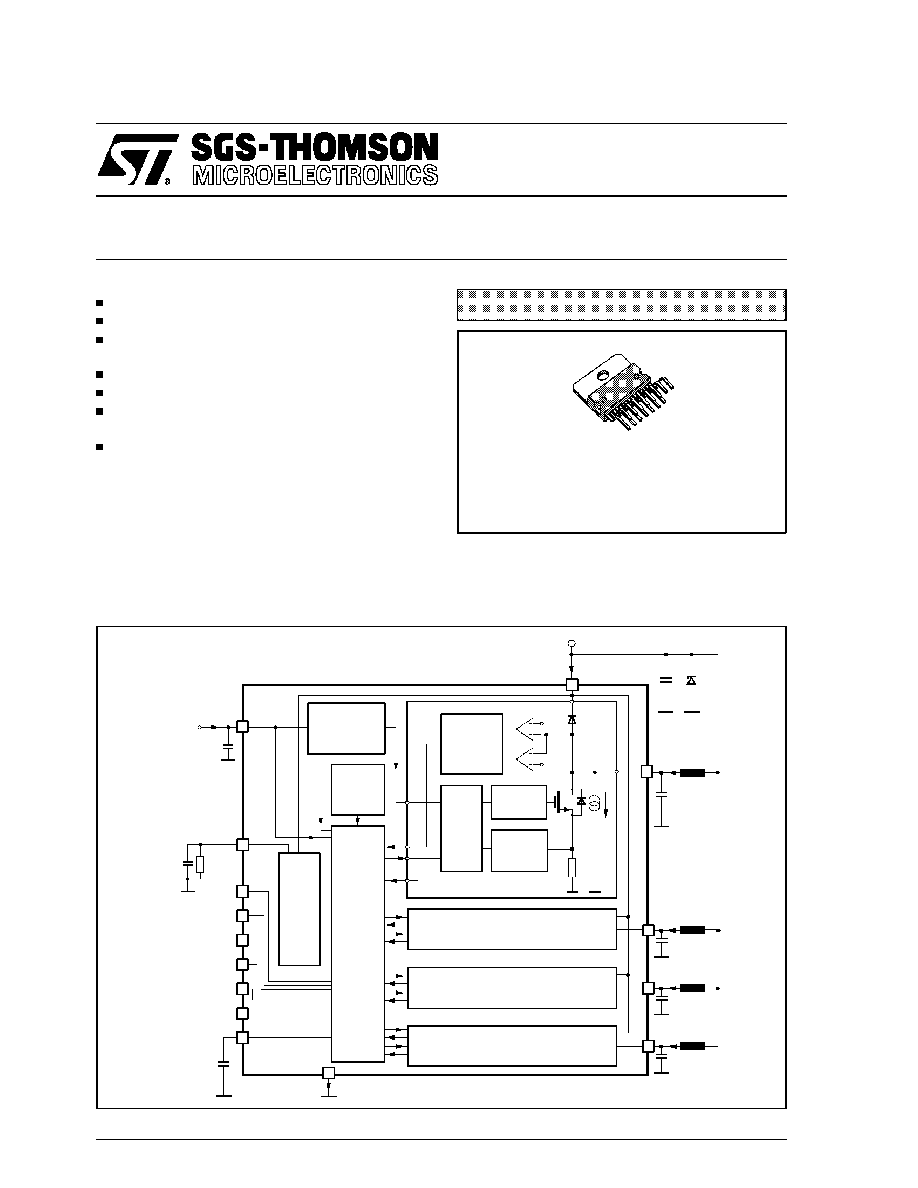
DESCRIPTION
The L9341 is a monolithic integrated circuit real-
ized in Multipower BCD-II mixed technology. The
driver is intended for inductive loads in synchro-
nous PWM applications, especially for valve driv-
ers. The output voltage and current rise and fall
slopes du/dt and di/dt are controlled.
This is advanced information on a new product now in development or undergoing evaluation. Details are subject to change without notice.
March 1994
UNDERVOLTAGE
SHUTDOWN
DIAGNOSTIC
DRIVER
SHORT
CURRENT
PROTECTION
CHANNEL 1
CHANNEL 4
CHANNEL 3
CHANNEL 2
V
flyth
V
offth
COMP1
COMP2
I
OSC
SDO
SDI
SCLK
RES1
SERIAL
INTERFACE
&
PWM
CONTROLL
BIAS
7
1
15
14
8
6
13
5
11
RES2
3
10
9
12
REXT
CS
4
OUT3
OUT4
GND
VS
V
s
I
Is
cc
I
OUT1
I
I
OUT2
OUT3
IOUT4
OSC
C
I
GND
C
BAT
D
BAT
Vcc
C
O1
C
O2
C
C
O3
O4
OUT2
VCC
2
outs
OUT1
di / dt & du / dt
CONTROL
THERMAL
FLAG
220nF
10nF
10nF
10nF
10nF
10uF
R ext
12.4k
10nF
BLOCK & APPLICATION DIAGRAM
Multiwatt 15
ORDERING NUMBERS: L9341V
L9341H
MULTIPOWER BCD TECHNOLOGY
1/10
ABSOLUTE MAXIMUM RATINGS
Symbol
Parameter
Value
Unit
V
CC
V
CC
Voltage Range
-0.3 to 6
V
V
S
V
S
Voltage Range
-0.3 to 24
V
V
spmax
VS Voltage Range for t
400ms
-2 to 40
V
V
st
Schaffner Transient Pulses on V
S
see note 1
V
Vin
Input Voltage Range for SDI; SCLK;CS;RES1;RES2
-0.3to V
CC
+0.3
V
out
Output Voltage Range for all Outputs:
Negative
Positive
≠ 0.3
intern. clamped to V
S
V
V
I
out
Output Current for all Outputs:
Negative
Positive
≠ 2
+ 2
A
A
for Transient with t < 10ms
Negative
Positive
≠ 5
5
A
A
Schaffner Transient Pulses on Output
see note 2
V
ESD
ESD Voltage Capability (MIL 883 C)
1500
V
THERMAL DATA
Symbol
Parameter
Value
Unit
R
th j-case
Thermal Resistance Junction to Case
3
∞
C/W
R
th j-amb
Thermal Resistance Junction to Ambient mounted on PC Board
35
∞
C/W
T
sdh
Thermal Hysteresis
20
∞
C
T
sd
Thermal Diagnostic
T
j
> 150
∞
C
Notes:
1. Schaffner transient specification: DIN 40839 test waveforms of the following type: 1, 2, 3a, 3b, 5 and 6.
The pulses are applied to the application circuit according to fig. 3.
2. The maximum output current results from the Schaffner pulses specified in note 1.
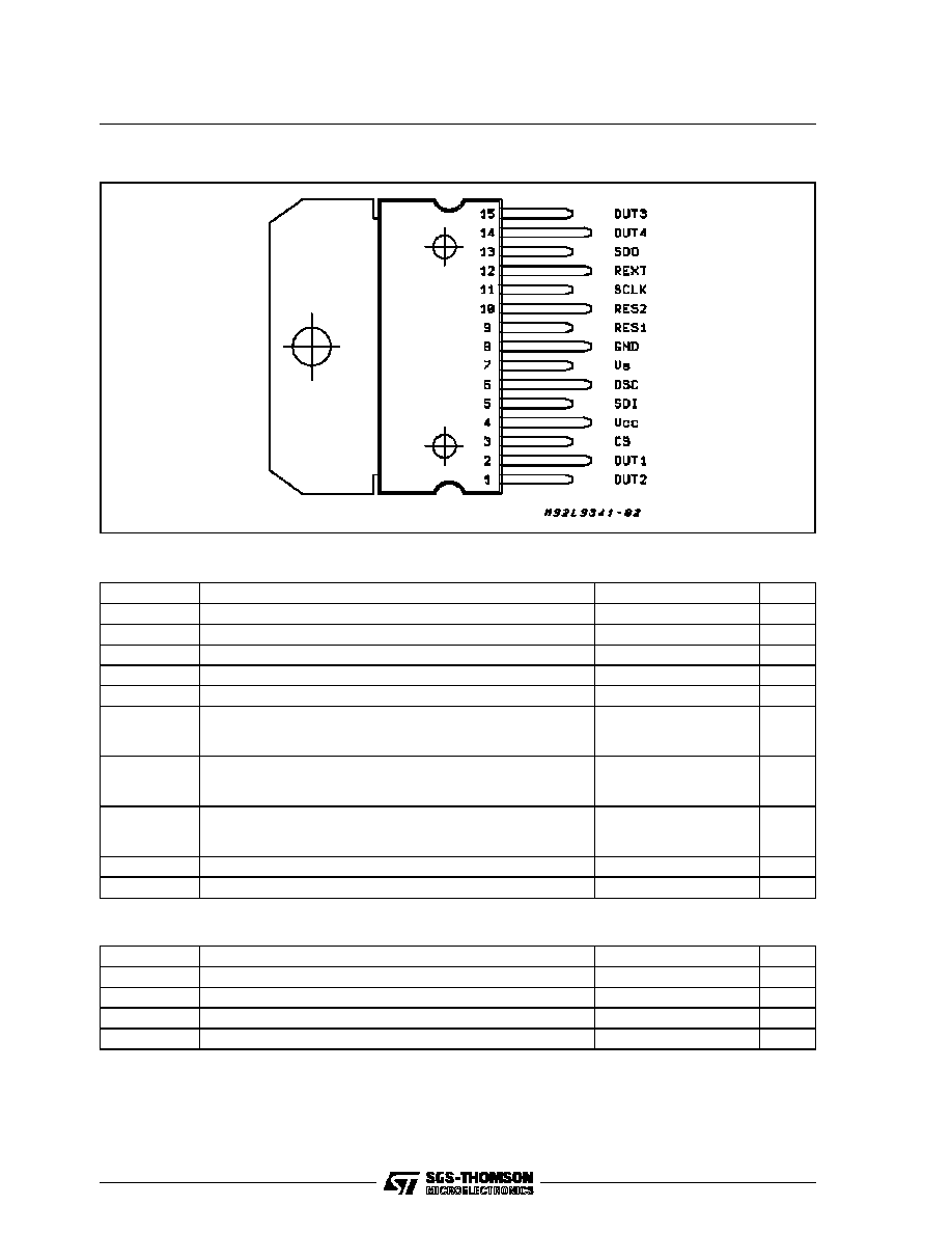
PIN CONNECTION (Top view)
L9341
2/10

ELECTRICAL CHARACTERISTICS (Unless otherwise specified: 8V
V
S
24V; 4.7V
V
CC
5.3V; ≠
40
∞
C
Tj
150
∞
C; I
O
1A (note 3); I
O
1.5A; V
sp
= V
S
for t
400ms; V
OUTP
= V
OUT
for t
400ms;
R
ext
= 12.4K
±
1%).
Symbol
Parameter
Test Condition
Min.
Typ.
Max.
Unit
I
ccq
V
cc
Quiescent Current
All Outputs Off
1
3
mA
I
sq
V
s
Quiescent Current
All Outputs Off
14
25
mA
V
ccu
V
cc
Undervoltage Threshold
See Note 4
3
4
4.7
V
V
cc r
V
cc
Range for RES1 and RES2
Operation
3
V
R
on
On Resistance
I
o
= 1A
T
j
= 125
∞
C
T
j
= 25
∞
C
750
450
m
m
I
o off
Off State Output Current
Outputs Off
1.4V
V
o
V
s
V
outp
= V
sp
= 40V
1
1
2.5
4
10
mA
mA
V
outf
Output Voltage During Flyback
I
o
= 1A Output Off
T
j
= 25
∞
C
T
j
= 125
∞
C
V
s
+1.3
V
s
+1.1
V
V
I
gndf
Current to GND during Flyback
(see note 5)
I
o
= 1A Output Off
V
s
= 24V
V
sp
= 40V
17
20
44
52
mA
mA
I
out r
Reverse Leakage Current
V
sp
- V
o
= 40V
500
µ
A
V
inH
High Input Level of SCLK,
SDI, CS, RES1, RES2
0.7*V
cc
V
cc
+0.3
V
V
inL
Low Input Level of SCLK,
SDI, CS, RES1, RES2
≠ 0.3
0.3*Vcc
V
V
REShys
Hysteresis of Reset Inputs
RES1, RES2
0.3
1
V
I
inRESH
Input Current on RES1,RES2
RES
i
= H; -2V
V
sp
8V
RES
i
= H; 8V
V
sp
40V
≠ 10
5
10
10
µ
A
µ
A
I
in
Input Current on SCLK,SDI,CS
≠ 2V
Vsp
40V
≠ 10
10
µ
A
V
SDOH
High Level SDO Output Voltage
I
SDO
= -1mA -2V
V
sp
40V
0.9*V
cc
V
cc
V
V
SDOL
Low Level SDO Output Voltage
I
SDO
= 1mA -2V
V
sp
40V
0
0.4
V
I
SDOZ
SDO Tristate High-Z Leakage
Current
0
V
SDO
V
cc
≠ 2V
V
sp
40V
≠ 10
10
µ
A
PWM
duty
PWM Duty Cycle
1/16
15/16
K
f
Frequency Accuracy Constant
See Note 6
0.93*K
fn
K
fn
1.07*K
fn
V
flyth
Flyback Diagnostic Comparator
Threshold
40
V
sp
8V
V
s
8V
V
s
≠ 1
1.5
V
s
≠ 0.4
V
V
V
offth
Off State Diagnostic
Comparator Threshold
1.5
2
V
I
outl
Output Current Limitation Threshold
see Note 7
1.5
2.5
A
t
dpo
Delay Time PWM Signal to Out.
5
15
µ
s
S
ov
Output Voltage Rise and Fall
Slope | du/dt |
(from 10 to 90% of V
o
) Fig. 2
1.0
10
V/
µ
s
S
oc
Output Current Rise and Fall
Slope |di/dt|
0.1
Io
1.5A
(from 10 to 90% of I
o
)
25
125
mA/
µ
s
Notes:
3. The mean value is I
o
=
1
T
I
o
(
t
)
dt
0
T
;
4. The outputs are switced off for Vcc
Vccu. The logic is not reseted. For a reset, RES1 or RES2 must be used.
5. This current is measured in the GND - terminal when one single output is in flyback and consists of the supply current added to the value
of the output current source and the leakage current of the flyback diode. This leakage current is less than 1% of the nominal flyback current.
6. The PWM frequency is defined by an external capacitor. The PWM oscillator frequency is: f
pwm
=
f
osc
32
with f
osc
=
K
f
C
osc
1A/V and k
in
= 15
10
- 6
;
the range is: 300Hz
f
pwm
3000Hz. The OSC Pin can be alternatively driven by an external TTL / CMOS signal.
7. For I
out
I
outl
an internal comparator switches the corresponding output off for the current PWM cycle.
L9341
3/10
15
CLK
PWM3
PWM4
PWM1
PWM2
14
13
12
11
10
9
8
7
6
5
4
3
2
1
0
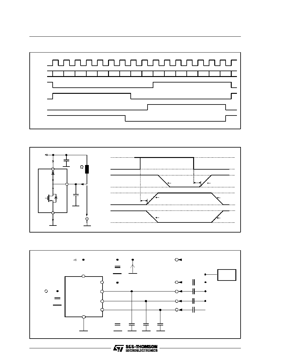
Figure 1: Logic Diagram of PWM Generation.
+12V
I s
I s
12V
0
1A
1A
0
0
du/dt
du/dt
di/dt
di/dt
di/dt
di/dt
5%
5%
Internal PWM Signal
I
I
Current through
Flyback Diode
Current through
Low Side Switch
I
GND
out
V out
t
dpo
out
t
dpo
f
I
f
D
DMOS
D
OUT
Vs
D
I
f
Output Voltage V
20 mH
5
10 nF
220 nF
Figure 2: Output Switching Diagram.
220 nF
D1
Schaffner
Generator
4 x 10 nF
-2V to 40 V
Vs
GND
OUT1
OUT2
OUT3
OUT4
4 x 1 nF
+12V
10 uF
VCC
+5V
Figure 3: Test Circuit for Schaffner Pulses.
INTERNAL
CLOCK
L9341
4/10

MSB
14
13
12
11
3
2
1
LSB
MSB
14
13
12
11
3
2
1
LSB
SCLK
SDI
SDO
CS
SCLK
SDI
SDO
tclcl
tchcl
tch
tcl
tclch
tchch
t su
th
t d
t clz
t oh
t zch
15
14
0
0
15
CS
Figure 4: Synchronous Serial Interface Protocol.
f
clock
Clock Frequency
min. DC
max. 2MHz
t
ch
Width of Clock Input High Puls
min. 200ns
t
cl
Widh of Clock Input Low Puls
min. 200ns
t
cicl
Clock Low Before CS Low
min. 200ns
t
chcl
Clock High After CS Low
min. 200ns
t
clch
Clock Low Before CS High
min. 200ns
t
chch
Clock High After CS High
min. 200ns
t
ciz
SDO Low-Z CS Low
min. 0ns
max. 400ns
t
zch
SDO High-Z CS High
max. 400ns
t
su
SDI Input Setup Time
min. 80ns
t
h
SDI Input Hold Time
min. 80ns
t
d
SDO Output Delay Time (C
L
= 50pF)
max. 100ns
t
oh
SDO Output Hold Time
min. 0ns
L9341
5/10

Bit 3 - 0
PWM1
PWM2
PWM3
PWM4
OUTPUT
0000
15/16
15/16
15/16
15/16
OFF
0001
1/16
15/16
1/16
15/16
ON
0010
2/16
14/16
2/16
14/16
ON
0011
3/16
13/16
3/16
13/16
ON
0100
4/16
12/16
4/16
12/16
ON
0101
5/16
11/16
5/16
11/16
ON
0110
6/16
10/16
6/16
10/16
ON
0111
7/16
9/16
7/16
9/16
ON
1000
8/16
8/16
8/16
8/16
ON
1001
9/16
7/16
9/16
7/16
ON
1010
10/16
6/16
10/16
6/16
ON
1011
11/16
5/16
11/16
5/16
ON
1100
12/16
4/16
12/16
4/16
ON
1101
13/16
3/16
13/16
3/16
ON
1110
14/16
2/16
14/16
2/16
ON
1111
15/16
1/16
15/16
1/16
ON
Figure 5: PWM Generation Function Table.
Bit. Nr.
Name
Contents
0
P10
PWM Duty Cycle for Channel 1 / Bit 0: LSB
1
P11
PWM Duty Cycle for Channel 1 / Bit 1
2
P12
PWM Duty Cycle for Channel 1 / Bit 2
3
P13
PWM Duty Cycle for Channel 1 / Bit 3 : MSB
4
P20
PWM Duty Cycle for Channel 2 / Bit 0 : LSB
5
P21
PWM Duty Cycle for Channel 2 / Bit 1 :
6
P22
PWM Duty Cycle for Channel 2 / Bit 2 :
7
P23
PWM Duty Cycle for Channel 2 / Bit 3 : MSB
8
P30
PWM Duty Cycle for Channel 3 / Bit 0 : LSB
9
P31
PWM Duty Cycle for Channel 3 / Bit 1 :
10
P32
PWM Duty Cycle for Channel 3 / Bit 2 :
11
P33
PWM Duty Cycle for Channel 3 / Bit 3 : MSB
12
P40
PWM Duty Cycle for Channel 4 / Bit 0 : LSB
13
P41
PWM Duty Cycle for Channel 4 / Bit 1:
14
P42
PWM Duty Cycle for Channel 4 / Bit 2 :
15
P43
PWM Duty Cycle for Channel 4 / Bit 3 : MSB
Figure 6: PWM Information From Microcontroller to QLSD.
L9341
6/10

Bit Nr.
Name
Contents
0
F11
COMP1 State at Positive Edge of PWM1 (0: V
out1
> V
flyth
; 1: V
out1
< V
flyth
)
1
F12
COMP2 State at Negative Edge of PWM1 (1: V
out1
> V
off th
; 0 : V
out1
< V
ofth
)
2
F21
COMP1 State at Positive Edge of PWM2 (0: V
out2
> V
flyth
; 1: V
out2
< V
flyth
)
3
F22
COMP2 State at Negative Edge of PWM2 (1: V
out2
> V
oft h
; 0 : V
out2
< V
ofth
)
4
F31
COMP1 State at Positive Edge of PWM3 (0: V
out3
> V
flyth
; 1: V
out3
< V
flyth
)
5
F32
COMP2 State at Negative Edge of PWM3 (1: V
out3
> V
off th
; 0 : V
out3
< V
ofth
)
6
F41
COMP1 State at Positive Edge of PWM4 (0: V
out4
> V
flyth
; 1: V
out4
< V
flyth
)
7
F42
COMP2 State at Negative Edge of PWM4 (1: V
out4 > Voffth
; 0 : V
out4
< V
ofth
)
8
RES1
Logic State of RES1 Input (0: RES1 = L ; 1: RES1 = H)
9
RES2
Logic State of RES2 Input (0: RES2 = L ; 1: RES2 = H)
10
TSDF
Thermal Diagnostic Flag ( 0: Overtemperature ; 1:Normal )
11
C1
Current at Negative Edge of PWM1 ( 0: I
out
> I
outl
; 1: I
out
< I
outl
)
12
C2
Current at Negative Edge of PWM2 ( 0: I
out
> I
outl
; 1: I
out
< I
outl
)
13
C3
Current at Negative Edge of PWM3 ( 0: I
out
> I
outl
; 1: I
out
< I
outl
)
14
C4
Current at Negative Edge of PWM4 ( 0: I
out
> I
outl
; 1: I
out
< I
outl
)
15
1
Framing Information (always 1)
Figure 7: Diagnostic Information from QLSD to Microcontroller.
PWM
V OUT
PWM
V
OUT
I D
t
C
tV
dPO
PWMON
t
t
min
Sample point COMP2
Sample point COMP1
dPO
t
tV
PWMOFF
t
min
Sample point COMP2
Sample point COMP1
Fig.1
Fig.2
Figure 8.
Fig. A
Fig. B
Note:
For safty diagnostic take notice of the following conditions:
t
PWMON
t
dPOMAX
+ t
C
+ t
V
(see Fig. A)
t
C
=
I
D
S
OCMIN
t
V
=
V
outfmax
S
OVMIN
t
PWMOFF
t
dPOMAX
+ t
V
(see Fig. B)
L9341
7/10

FUNCTIONAL DESCRIPTION
The U511 is a PWM quad low side driver for in-
ductive loads. The duty cycle of the internal gen-
erated PWM signal is set by a microcontroller via
a serial interface for each output. An output slope
limitation for both dv/dt and di /dt is implemented
to reduce RFI. The PWM generation is realized
avoiding a simultaneous output switching. As a
result, di/dt becomes smaller. Integrated flyback
diodes clamp the output voltage during the fly-
back phase of the low side switches.
The driver is protected against short circuit. An
undervoltage shutdown circuit switches off all out-
puts if V
cc
is less then V
ccu
. Below the shutdown
voltage all outputs remain in off state regardless
of the input state. After each malfunction which
resets the driver, only the serial link interface can
reactivate the normal function. In case of overcur-
rent (I
out
= I
out1
), an internal comparator switches
the output off. The overcurrent information can be
read via the serial link for each driver separately
at the negative edge of the corresponding PWM
signal.
The interface to the microcontroller is realized
with a 16 bit synchronous serial peripheral inter-
face (SPI). If CS is switched low, the serial link
becomes active and SDO goes to low impedance.
At the rising edge of the SCLK signal, one of the
16 bit of data stored in a shift register appear se-
quencely at SDO. These data contain the 8 error
flags, the status of thermal diagnostic flag and the
external reset sources RES1, RES2 and the over-
current flgs c1...c4. The last bit is framing infor-
mation (see fig. 7). At each falling edge of SCLK,
one of the 16 bits of data sent by the microcon-
troller is transferred via the SDI input to the driver.
These data contain the duty-cycle information for
the internal PWM generation (4 times 4 bit).
On the rising edge of CS the previously stored in-
formation is transferred to the circuits. SDO be-
come now high impedance and SDI is inactive.
The serial interface of the QLSD is cascadable
with the serial link interface of another QLSD,
thus obtaining a 32 bit serial link information wich
can control eight inductive loads. For a safety
data transfer the takeover of data bits is only real-
ized when the number of SCLK - clocks is n x 16
(n
1).
The PWM duty cycle is set by 4 bit for each out-
put independently via the serial link. If all four bits
for an output are zero, the output is turned off, but
the error diagnosis will work correctly (see fig. 5
and 6). The PWM frequency is defined by an ex-
ternal capacitor on the OSC pin. Rext defines
through the reference current the output current
slope, the diagnostic current sink and the internal
oscillator frequency (together with C
osc
).
For error diagnosis the voltage on the output is
measured during the on and off state of the par-
ticular output driver. Upon the rising edge of the
PWM signal (at this moment the power output is
off and will be switched on) the status of COMP1
is stored into an internal latch. On the falling edge
of the PWM signal ( the power output is on and
will be switched off) the status of COMP2 is
stored into another internal latch. This information
can be read via the serial link for each output
driver separately (see fig. 7).
The thermal diagnostic switch the thermal flag to
0 in case of overtemperature T
T
sd
. It will be
switched to 1 with the hysteresis T
sdth
in case of
T < T
sd
- T
sdh
.
To avoid male functions due to extensive noise or
spikes at the supply pins V
CC
, V
S
and R
ext
must
be blocked externally via capacitors.
L9341
8/10
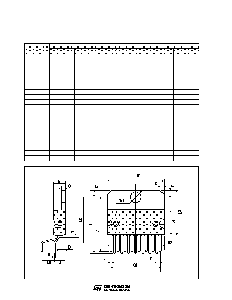
MULTIWATT15 PACKAGE MECHANICAL DATA
DIM.
mm
inch
MIN.
TYP.
MAX.
MIN.
TYP.
MAX.
A
5
0.197
B
2.65
0.104
C
1.6
0.063
D
1
0.039
E
0.49
0.55
0.019
0.022
F
0.66
0.75
0.026
0.030
G
1.02
1.27
1.52
0.040
0.050
0.060
G1
17.53
17.78
18.03
0.690
0.700
0.710
H1
19.6
0.772
H2
20.2
0.795
L
21.9
22.2
22.5
0.862
0.874
0.886
L1
21.7
22.1
22.5
0.854
0.870
0.886
L2
17.65
18.1
0.695
0.713
L3
17.25
17.5
17.75
0.679
0.689
0.699
L4
10.3
10.7
10.9
0.406
0.421
0.429
L7
2.65
2.9
0.104
0.114
M
4.25
4.55
4.85
0.167
0.179
0.191
M1
4.63
5.08
5.53
0.182
0.200
0.218
S
1.9
2.6
0.075
0.102
S1
1.9
2.6
0.075
0.102
Dia1
3.65
3.85
0.144
0.152
L9341
9/10

Information furnished is believed to be accurate and reliable. However, SGS-THOMSON Microelectronics assumes no responsibility for the
consequences of use of such information nor for any infringement of patents or other rights of third parties which may result from its use. No
license is granted by implication or otherwise under any patent or patent rights of SGS-THOMSON Microelectronics. Specifications men-
tioned in this publication are subject to change without notice. This publication supersedes and replaces all information previously supplied.
SGS-THOMSON Microelectronics products are not authorized for use as critical components in life support devices or systems without ex-
press written approval of SGS-THOMSON Microelectronics.
©
1994 SGS-THOMSON Microelectronics - All Rights Reserved
SGS-THOMSON Microelectronics GROUP OF COMPANIES
Australia - Brazil - France - Germany - Hong Kong - Italy - Japan - Korea - Malaysia - Malta - Morocco - The Netherlands - Singapore -
Spain - Sweden - Switzerland - Taiwan - Thaliand - United Kingdom - U.S.A.
L9341
10/10