 | –≠–ª–µ–∫—Ç—Ä–æ–Ω–Ω—ã–π –∫–æ–º–ø–æ–Ω–µ–Ω—Ç: L93PI | –°–∫–∞—á–∞—Ç—å:  PDF PDF  ZIP ZIP |
74LVQ14
HEX SCHMITT INVERTER
Æ
February 1999
s
HIGH SPEED: t
PD
= 6 ns (TYP.) at V
CC
= 3.3V
s
COMPATIBLE WITH TTL OUTPUTS
s
LOW POWER DISSIPATION:
I
CC
= 2
µ
A (MAX.) at T
A
= 25
o
C
s
LOW NOISE:
V
OLP
= 0.3 V (TYP.) at V
CC
= 3.3V
s
75
TRANSMISSION LINE DRIVING
CAPABILITY
s
SYMMETRICAL OUTPUT IMPEDANCE:
|I
OH
| = I
OL
= 12 mA (MIN)
s
PCI BUS LEVELS GUARANTEED AT 24mA
s
BALANCED PROPAGATION DELAYS:
t
PLH
t
PHL
s
OPERATING VOLTAGE RANGE:
V
CC
(OPR) = 2V to 3.6V
s
PIN AND FUNCTION COMPATIBLE WITH
74 SERIES 14
s
IMPROVED LATCH-UP IMMUNITY
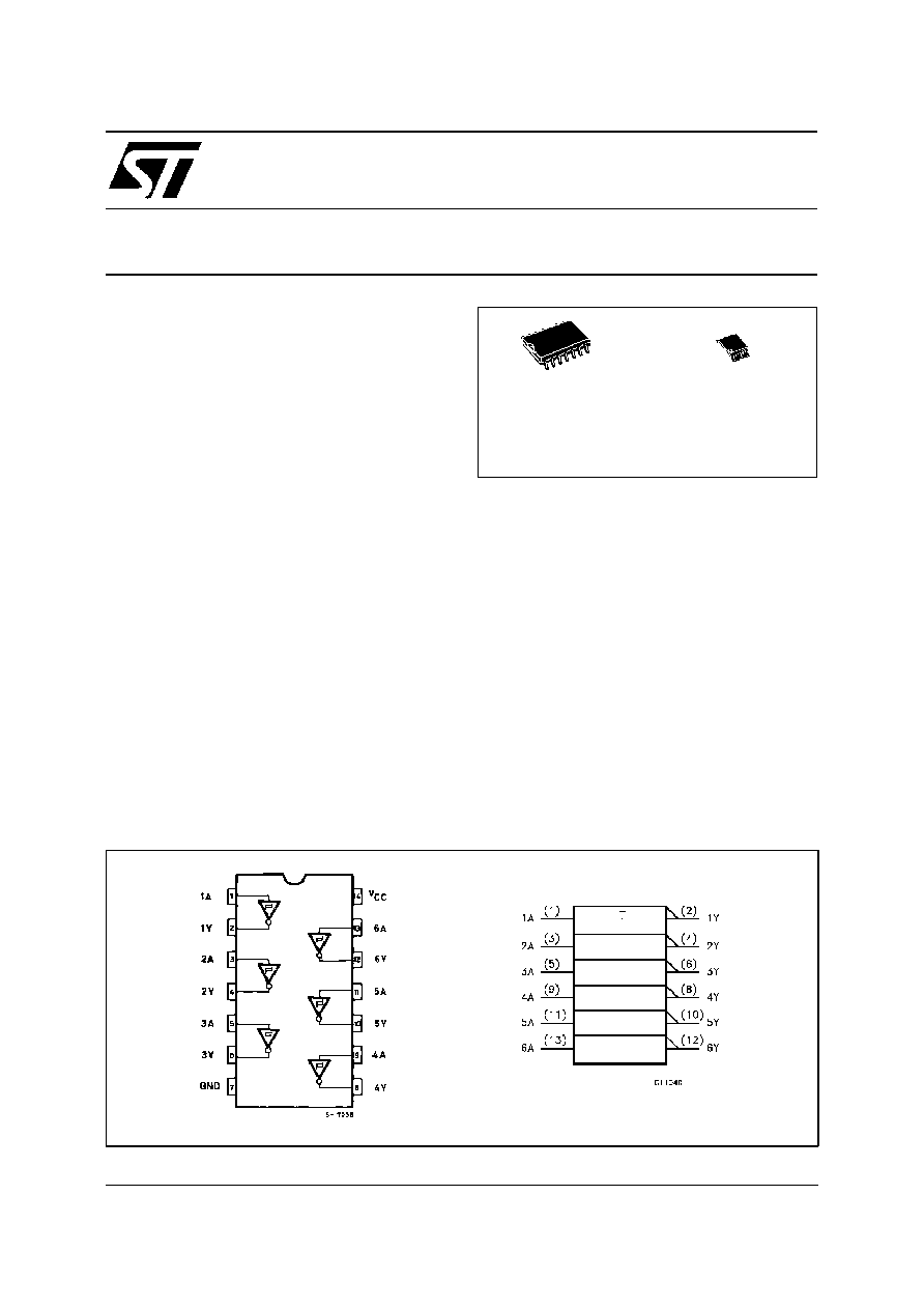
DESCRIPTION
The LVQ14 is a low voltage CMOS HEX
SCHMITT INVERTER fabricated with sub-micron
silicon gate and double-layer metal wiring C
2
MOS
technology. It is ideal for low power and low noise
3.3V applications.
The internal circuit is composed of 3 stages
including buffer output, which enables high noise
immunity and stable output.
It has better speed performance at 3.3V than 5V
lsttl family combined with the true CMOS low
power consumption.
Pin configuration and function are the same as
those of the LVQ04 but the LVQ14 has hysteresis
between the positive and negative input threshold
typically of 1V.
This together with its schmitt trigger function
allows it to be used on line receivers with slow
rise/fall input signals.
All inputs
and
outputs are
equipped with
protection circuits against static discharge, giving
them 2KV ESD immunity and transient excess
voltage.
PIN CONNECTION AND IEC LOGIC SYMBOLS
ORDER CODES :
74LVQ14M
74LVQ14T
M
(Micro Package)
T
(TSSOP Package)
1/8
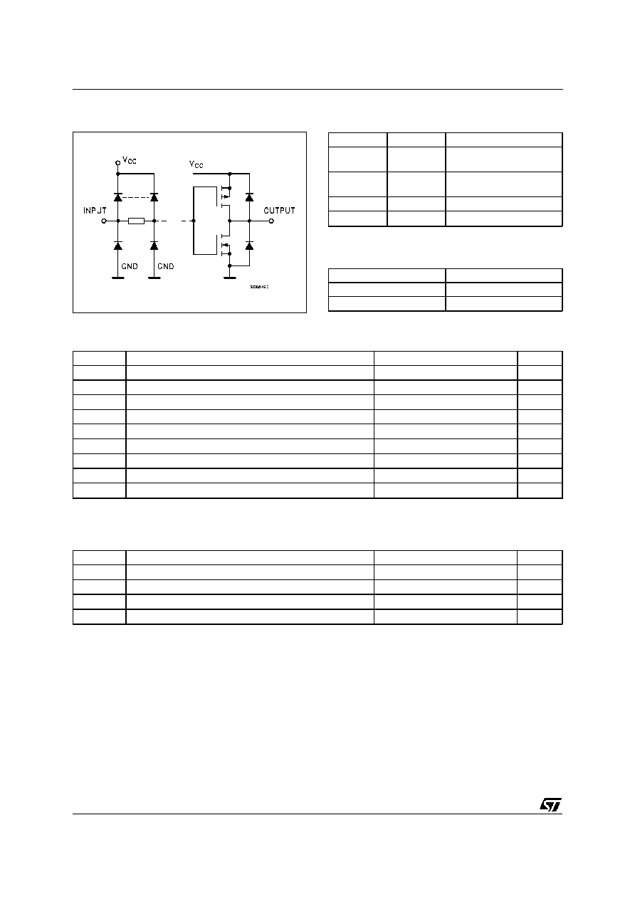
INPUT AND OUTPUT EQUIVALENT CIRCUIT
ABSOLUTE MAXIMUM RATINGS
Symbol
Parameter
Val ue
Unit
V
CC
Supply Voltage
-0.5 to +7
V
V
I
DC Input Voltage
-0.5 to V
CC
+ 0.5
V
V
O
DC Output Voltage
-0.5 to V
CC
+ 0.5
V
I
IK
DC Input Diode Current
±
20
mA
I
OK
DC Output Diode Current
±
20
mA
I
O
DC Output Current
±
50
mA
I
CC
or I
GND
DC V
CC
or Ground Current
±
300
mA
T
stg
Storage Temperature
-65 to +150
o
C
T
L
Lead Temperature (10 sec)
300
o
C
Absolute Maximum Ratings are those values beyond which damage to the device may occur. Functional operation under these condition is not implied.
TRUTH TABLE
A
Y
L
H
H
L
PIN DESCRIPTION
PI N No
SYMBOL
NAME AND FUNCT ION
1, 3, 5, 9,
11, 13
1A to 6A
Data Inputs
2, 4, 6, 8,
10, 12
1Y to 6Y
Data Outputs
7
GND
Ground (0V)
14
V
CC
Positive Supply Voltage
RECOMMENDED OPERATING CONDITIONS
Symbol
Parameter
Valu e
Uni t
V
CC
Supply Voltage (note 1)
2 to 3.6
V
V
I
Input Voltage
0 to V
CC
V
V
O
Output Voltage
0 to V
CC
V
T
op
Operating Temperature:
-40 to +85
o
C
1) Truth Table guaranteed: 1.5V to 3.6V
74LVQ14
2/8
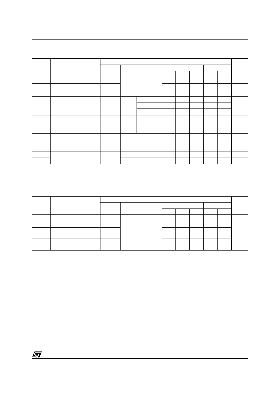
DC SPECIFICATIONS
Symb ol
Parameter
Test Co nditi ons
Valu e
Un it
V
CC
(V)
T
A
= 25
o
C
-40 to 85
o
C
Min.
T yp.
Max.
Mi n.
Max.
V
t+
Positive Input Threshold
3.0
2.2
2.2
V
V
t-
Negative Input Threshold
3.0
0.9
0.9
V
V
H
Hysteresis Voltage
3.0
0.3
1.2
0.3
1.2
V
V
OH
High Level Output
Voltage
3.0
V
I
(* )
=
V
IL
I
O
=-50
µ
A
2.9
2.99
2.9
V
I
O
=-12 mA
2.58
2.48
I
O
=-24 mA
2.2
V
OL
Low Level Output
Voltage
3.0
V
I
(* )
=
V
IH
I
O
=50
µ
A
0.002
0.1
0.1
V
I
O
=12 mA
0
0.36
0.44
I
O
=24 mA
0.55
I
I
Input Leakage Current
3.6
V
I
= V
CC
or GND
±
0.1
±
1
µ
A
I
CC
Quiescent Supply
Current
3.6
V
I
= V
CC
or GND
2
20
µ
A
I
OLD
Dynamic Output Current
(note 1, 2)
3.6
V
OLD
= 0.8 V max
36
mA
I
OHD
V
OHD
= 2 V min
-25
mA
1) Maximum test duration 2ms, one output loaded attime
2) Incident wave switching is guaranteed on transmission lines with impedances as low as 50
.
(*) All outputs loaded.
DYNAMIC SWITCHING CHARACTERISTICS
Symb ol
Parameter
Test Co nditi ons
Valu e
Un it
V
CC
(V)
T
A
= 25
o
C
-40 to 85
o
C
Min.
T yp.
Max.
Mi n.
Max.
V
OLP
Dynamic Low Voltage
Quiet Output (note 1, 2)
3.3
C
L
= 50 pF
0.3
0.8
V
V
OLV
-0.8
-0.3
V
IHD
Dynamic High Voltage
Input (note 1, 3)
3.3
2
V
IL D
Dynamic Low Voltage
Input (note 1, 3)
3.3
0.8
1) Worst case package.
2) Max number of outputs defined as (n). Data inputs are driven 0V to 3.3V, (n -1) outputs switching and one output at GND.
3) Max number of data inputs (n) switching. (n-1) switching 0V to3.3V. Inputs under test switching: 3.3V to threshold (V
ILD
), 0V to threshold (V
IHD
).,f=1MHz.
74LVQ14
3/8
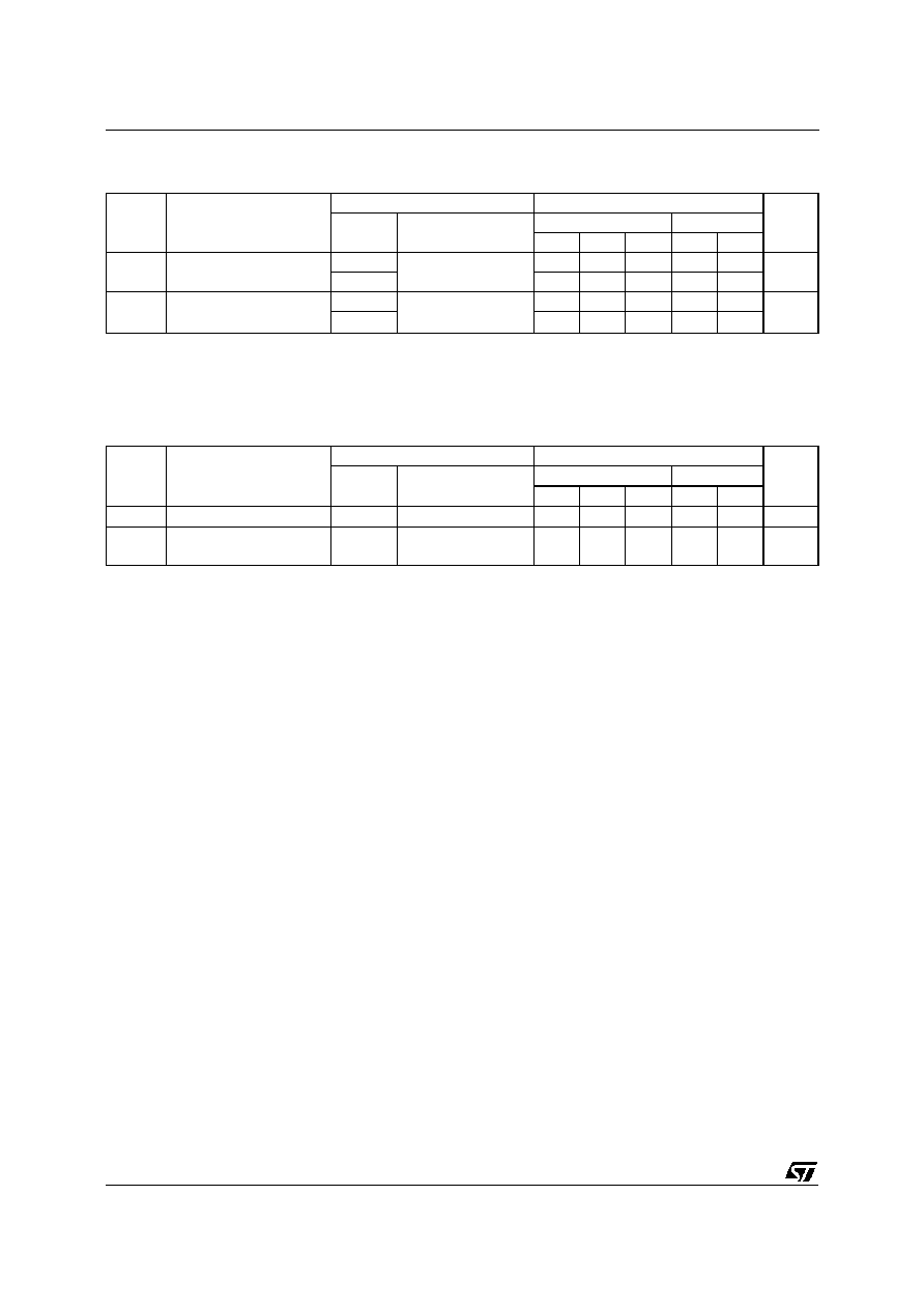
CAPACITIVE CHARACTERISTICS
Symb ol
Parameter
Test Co nditi ons
Valu e
Un it
V
CC
(V)
T
A
= 25
o
C
-40 to 85
o
C
Min.
T yp.
Max.
Mi n.
Max.
C
IN
Input Capacitance
3.3
4
pF
C
PD
Power Dissipation
Capacitance (note 1)
3.3
f
IN
= 10 MHz
29
pF
1) C
PD
isdefined as the value of the IC'sinternal equivalent capacitance which is calculated fromthe operating current consumption without load. (Referto
Test Circuit).Average operting current can be obtained by the following equation. I
CC
(opr) = C
PD
∑
V
CC
∑
f
IN
+ I
CC
/6(per gate)
AC ELECTRICAL CHARACTERISTICS (C
L
= 50 pF, R
L
= 500
, Input t
r
= t
f
=3 ns)
Symb ol
Parameter
T est Con ditio n
Valu e
Un it
V
CC
(V)
T
A
= 25
o
C
-40 to 85
o
C
Min.
T yp.
Max.
Mi n.
Max.
t
PLH
t
PHL
Propagation Delay Time
2.7
7.0
16.0
19.0
ns
3.3
(*)
6.0
11.5
13.0
t
OSLH
t
OSHL
Output to Output Skew
Time (note 1, 2)
2.7
0.5
1.0
1.5
ns
3.3
(*)
0.5
1.0
1.5
1) Skew is defined as the absolute value of the difference between the actual propagation delay for any twooutputs of the same device switching in the
same direction, either HIGH or LOW
2) Parameter guaranteed by design
(*) Voltage range is 3.3V
±
0.3V
74LVQ14
4/8
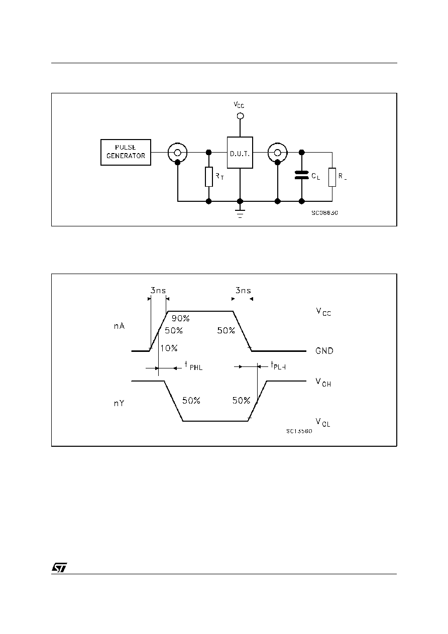
TEST CIRCUIT
C
L
= 50 pF or equivalent (includes jigand probe capacitance)
R
L
= R
1
= 500
orequivalent
R
T
= Z
OUT
of pulse generator (typically 50
)
WAVEFORM: PROPAGATION DELAYS (f=1MHz; 50% duty cycle)
74LVQ14
5/8