 | –≠–ª–µ–∫—Ç—Ä–æ–Ω–Ω—ã–π –∫–æ–º–ø–æ–Ω–µ–Ω—Ç: L9638 | –°–∫–∞—á–∞—Ç—å:  PDF PDF  ZIP ZIP |

1/14
L9638
October 2004
1
FEATURES
Single-wire transceiver for LIN-protocol
Transmission rate up to 20 kbaud
Operating power supply voltage range 6V
Vs
26V (40V for transients)
Low quiescent current in sleep mode (typ.10
µA)
Wake-up through LIN-bus, Enable input (from
µC CMOS compatible) or Wake-up input (edge
driven)
Wide input and output range -24V
V
LIN
Vs
Integrated pull/down/up resistors for LIN, TxD,
RxD, EN, INH
Inhibit output with low resistance (<40
) versus
Vs and short circuit protection
CMOS compatible TxD, RxD Interface
EMI robustness optimised
Thermal shutdown and LIN short circuit
protection
2
DESCRIPTION
The L9638 is a monolithic integrated circuit for
LIN-bus interface function between the protocol
handler in the controller and the physical bus in
automotive applications.
As well as it can be used in standard ISO 9141
systems.
SO-8
LIN BUS TRANSCEIVER
Figure 1. Block Diagram
VS
TxD
WUP
RxD
LIN
INH
EN
Internal
Voltage
Regulator
Int.5V
GND
Glitch
Filter
Glitch
Filter
VS_D
Control
Logic
Protection
VS_D
VS
TxD
WUP
RxD
LIN
INH
EN
Internal
Voltage
Regulator
Int.5V
GND
Glitch
Filter
VS
TxD
WUP
RxD
LIN
INH
EN
Internal
Voltage
Regulator
Int.5V
GND
Glitch
Filter
Glitch
Filter
VS_D
Control
Logic
Protection
VS_D
Table 1. Order Codes
Part Number
Package
L9638D
SO-8
L9638D013TR
Tape & Reel
Rev. 4

L9638
2/14
Table 2. Pin Description
Figure 2. Pin Connection
Table 3. Absolute Maximum Ratings
Table 4. Thermal Data
Pin No.
Pin Name
Function
1
RxD
Receive data Output
2
EN
Enable Input
Digital control signal for low power modes
3
WUP
Wake-Up Input
Local wake-up from sleep mode sensitive to positive and negative edges
4
TxD
Transmit data Input
5
GND
Ground
6
LIN
Bidirectional I/O
7
Vs
Supply voltage
8
INH
Inhibit Output, battery related high side switch for controlling external Voltage
Regulator
Symbol
Parameter
Value
Unit
V
S
Supply Voltage
-0.3 to 40
V
V
LIM
Pin Voltage
-24 to 40
V
V
INH ,
W
UP
Pin Voltage
-0.3 to 40
V
V
RxD ,
T
xD
, EN Pin Voltage
-0.3 to 6
V
V
ESD
HBM: all pins withstand ±2KV; pin 6 (LIN) is able to withstand
±8kV versus GND and +8/-5kV versus V
S
Symbol
Parameter
Value
Unit
T
J_OP
Operating junction temperature
-40 to150
∞C
R
th j-amb
Thermal steady state junction to ambient resistance
145
K/W
T
J_SD
Thermal shutdown temperature
170 ±20
∞C
T
stg
Storage temperature
-55 to 150
∞C
RxD
EN
WUP
TxD
GND
LIN
Vs
INH
1
3
2
4
6
5
7
8
D04AT514

3/14
L9638
Table 5. Electrical Characteristics
(V
S
= 6V to 26V; T
J
= -40 to 150 ∞C unless otherwise specified)
Item
Symbol
Parameter
Test Condition
Min.
Typ.
Max.
Unit
1
Supplies
1.1
V
S
Supply Voltage
6
26
V
1.2
I
Sleep
Supply Vs Curent in sleep
mode
V
EN
= V
EN low
10
30
µA
1.3
I
Short
Supply Vs Curent with bus
short circuit
V
EN
= V
EN low
150
500
1700
µA
1.4
I
DStand-by
Supply Vs Current in Stand-
by Mode with bus recessive
V
LIN
= V
LINHigh
V
EN
= V
ENLow
V
TxD
= V
TxDHigh
30
100
200
µA
1.5
I
DStand-by
Supply Vs Current in Stand-
by Mode with bus dominant
(Receive only Mode)
V
LIN
= V
LINLow
V
EN
= V
ENLow
0.5
1.1
2.5
mA
1.6
Is
Normal
Supply Vs Current in
Normal Mode with bus
recessive
V
EN
= V
ENHigh
V
LIN
= V
LINHigh
V
TxD
= V
TxDHigh
300
500
700
µA
1.7
Is
Normal
Supply Vs Current in
Normal Mode with bus
dominant
V
EN
= V
ENHigh
V
LIN
= V
LINLow
V
TxD
= V
TxDLow
0.9
1.8
3.5
mA
2
LIN Bus Interface
2.1
V
BUSDom
Receive Threshold Voltage
recessive to dominant state
V
LIN
<18V
0.4
0.45
0.5
Vs
2.2
V
BUSRec
Receive Threshold Voltage
dominant to recessive state
V
LIN
8V
0.5
0.55
0.6
Vs
2.3
V
HYS
Receive Threshold
Hysteresis
V
BUSRec
-V
BUSDom
0.05
0.1
0.17
Vs
2.4
V
BUScnt
Tolerance centre value of
Receiver
(VBUS
Rec
+VBUS
Dom
)/2
0.475
0.5
0.525
Vs
2.5
I
LINON
Input Current dominant
state
V
TxD
= V
TxDLow
V
LIN
= V
S
40
100
160
mA
2.5.1
I
LINOff
Input Current recessive
state
V
TxD
= V
TxDHigh
V
LIN
= V
s
-10
10
µA
2.5.2
I
LINOff
Input Current recessive
state
V
TxD
= V
TxDHigh
;
V
S
= 12V;
V
LIN
= 0V
(Bus dominant )
-1
mA
2.6
V
LINDom
Drive Voltage dominant
state
V
TxD
= V
TxDLow
I
LIN
= 40mA
1.2
V
2.7
R
LIN
Output pull up resistor
20
30
47
k
2.8
f
LIN-RxD
Transmission Frequency
R
Vs-LIN
=1100
C
LIN-GND
=10nF
20
kHz
2.9
d
VLIN/dt
Slew rate rising edge
From 10% to 90% of V
LIN
1
2
3
V/
µs

L9638
4/14
2.10
d
VLIN/dt
Slew rate falling edge
From 90% to 10% of V
LIN
-3
-2
-1
V/
µs
2.11
t
sym
Rising/ Falling edge
symmetry
t
sym
= t
slope_fall
- t
slope_rise
-5
-5
µs
2.12
t
trans_pd
Propagation delay of
transmitter
See Fig.2
t
trans_pd
= max (t
trans_pdr,
trans_pdf
)
4
µs
2.13
t
rec_pd
Propagation delay of
receiver
See Fig.2
t
rec_pd
= max (t
rec_pdr, trec_pdf
)
6
µs
2.14
t
rec_sym
Symmetry of receiver
propagation delay rising
edge w.r.t. falling edge
See Fig.2
t
rec_sym
= (t
rec_pdf -trec_pdr
)
-2
2
µs
2.15
t
trans_sym
Symmetry of transmitter
propagation delay rising
edge w.r.t. falling edge
See Fig.2
t
trans_sym
= (t
trans_pdf -ttrans_pdr
)
-2
2
µs
2.16
t
LINgs
Bus wake-up glitch
suppression time
See Fig.3 V
LIN
= V
LINLow
40
100
µs
3
Transmission Input TxD
3.1
VT
xDLow
Input Voltage dominant
state
1.5
V
3.2
VT
xDHigh
Input Voltage recessive
state
3.5
V
3.3
RT
xD
TxD pull up resistor
5
10
25
K
4
Receive Output RxD
4.1
VR
xDLow
Output Voltage dominant
state
I
RxD
= 2mA
1.5
V
4.2
VR
xDHigh
Output Voltage recessive
state
I
RxD
10µA
4.5
V
4.3
R
RxD
RxD pull up resistor
5
10
25
k
5
Inhibit Output INH
5.1
R
ON(INH)
Switch on resistance
between Vs and INH
I
INH
=-15mA; Vs=13.5V
20
40
5.2
I
ON(INH)
INH output current
Normal or stand-by mode
15
30
50
mA
5.3
R
OFF(INH)
Switch off INH pull down
resistor
5
10
25
k
6
Wake Up Input WUP
6.1
V
WUPLow
Low level input voltage
1.5
V
6.2
V
WUPHigh
High level input voltage
3.5
Vs+0.
3
V
Table 5. Electrical Characteristics (continued)
(V
S
= 6V to 26V; T
J
= -40 to 150 ∞C unless otherwise specified)
Item
Symbol
Parameter
Test Condition
Min.
Typ.
Max.
Unit

5/14
L9638
Note:
1. Room temperature evaluated - no 100% tested
6.3
t
WUPgs
Remote wake-up delay time
Transitioning on WUP
40
100
µs
7
Enable Input EN
7.1
VEN
Low
Low level input voltage
1.5
V
7.2
VEN
High
High level input voltage
3.5
V
7.3
R
EN
EN pull down resistor
5
10
25
K
7.4
tgts
Go to sleep delay time
V
EN
= V
ENlow
40
100
µs
7.5
t
ENgs
EN wake-up glitch
suppression time
V
EN
= V
ENhigh
40
100
µs
8
AC Timing Parameters
8.1
D1
Duty Cycle 1
TH
Rec(max)
= 0.744 x V
SUP
;
TH
Dom(max)
= 0.581 x V
SUP
;
Vsup = 7.0 to 18V; t
bit
= 50
µs;
D1 = t
Bus_rec(min)
/2 x t
Bit
(C
BUS
; R
BUS
) 1nF; 1k
/6.8nF;
660
/10nF; 500
0.396
8.2
D2
Duty Cycle 2
TH
Rec(min)
= 0.284 x V
SUP
;
TH
Dom(min)
= 0.422 x V
SUP
;
Vsup = 7.6 to 18V; t
bit
= 50
µs;
D2 = t
Bus_rec(min)
/2 x t
Bit
(C
BUS
; R
BUS
) 1nF; 1k
/6.8nF;
660
/10nF; 500
0.581
8.3
D3
Duty Cycle 3
TH
Rec(max)
= 0.778 x V
SUP
;
TH
Dom(max)
= 0.616 x V
SUP
;
Vsup = 7.0 to 18V; t
bit
= 96
µs;
D3 = t
Bus_rec(min)
/2 x t
Bit
(C
BUS
; R
BUS
) 1nF; 1k
/6.8nF;
660
/10nF; 500
0.417
8.4
D4
Duty Cycle 4
TH
Rec(min)
= 0.251 x V
SUP
;
TH
Dom(min)
= 0.389 x V
SUP
;
Vsup = 7.6 to 18V; t
bit
= 96
µs;
D4 = t
Bus_rec(min)
/2 x t
Bit
(C
BUS
; R
BUS
) 1nF; 1k
/6.8nF;
660
/10nF; 500
0.591
9
Fault Conditions
9.1
I
LIN_NO_GND
LIN current with GND
disconnected
GND = Vs = 12V
0V< V
LIM
< 18V
(1)
-1
1
mA
9.2
I
LIN_NO_Vs
LIN current with V
S
grounded
V = GND, 0V < V
LIN
< 18V
(1)
100
µA
Table 5. Electrical Characteristics (continued)
(V
S
= 6V to 26V; T
J
= -40 to 150 ∞C unless otherwise specified)
Item
Symbol
Parameter
Test Condition
Min.
Typ.
Max.
Unit

L9638
6/14
3
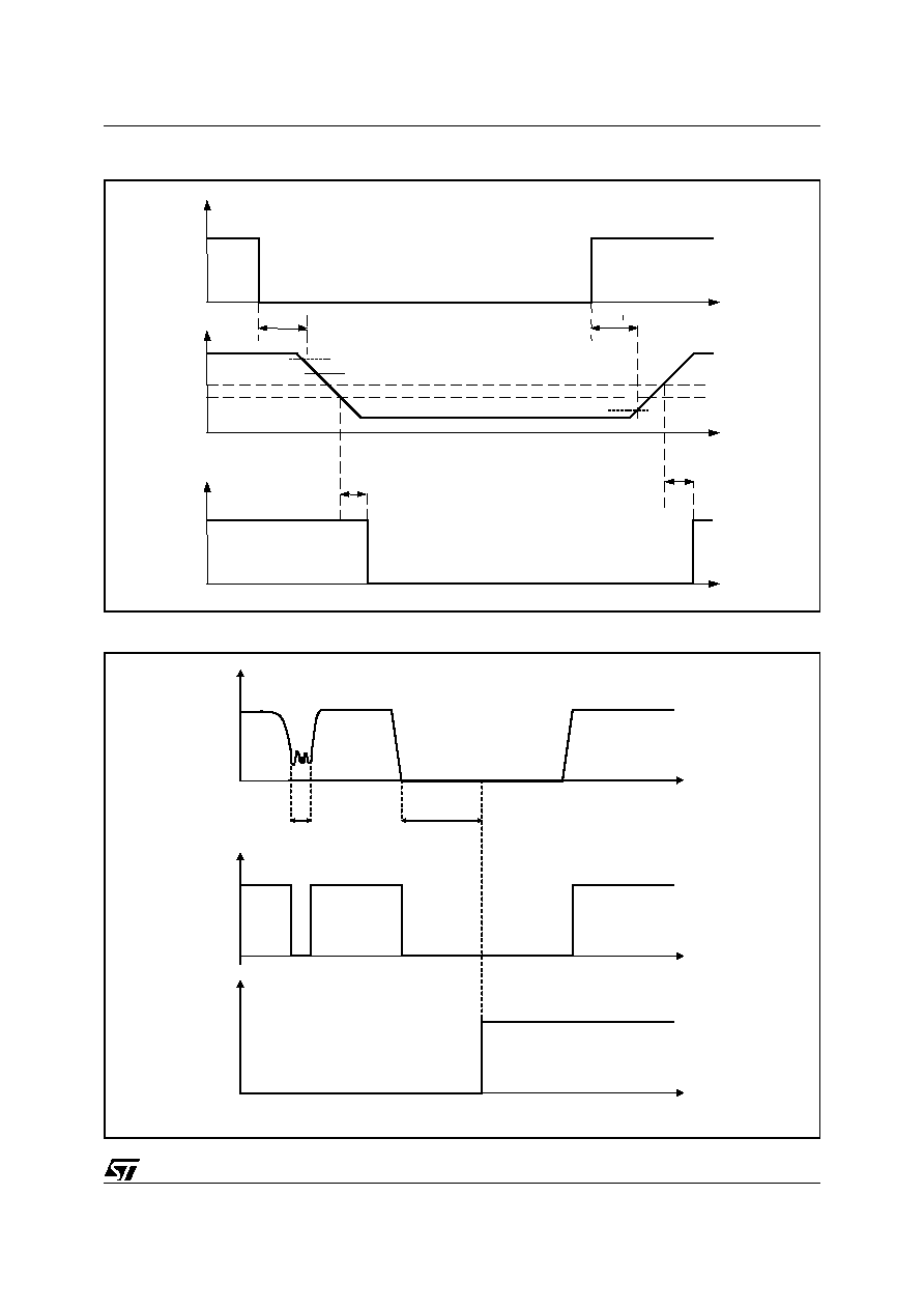
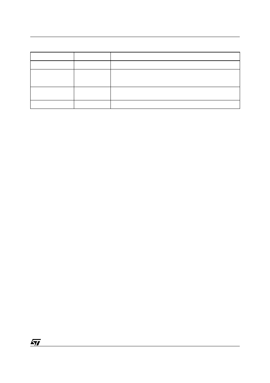
TIMING DIAGRAM
Figure 3. Definition of Bus Timing Parameters
7/14
L9638
Figure 4. Typical Bus Timing
Figure 5. Typical Wake-up Timing
t
V
TxD
t
V
LIN
t
V
RxD
t
trans_pdf
t
trans_pdr
Receive Dominant Threshold
Receive Recessive Threshold
t
rec_pdr
t
rec_pdf
90%
10%
t
V
TxD
t
V
LIN
t
V
RxD
t
trans_pdf
t
trans_pdr
Receive Dominant Threshold
Receive Recessive Threshold
t
rec_pdr
t
rec_pdf
90%
10%
V
LIN
t
t<t
LINgs
gs
t
LIN
V
RxD
t
V
INH
t

L9638
8/14
4
FUNCTIONAL DESCRIPTION
The L9638 is a monolithic bus driver designed to provide bidirectional serial communication in Local In-
terconnect Network (LIN).
In addition to the integrated physical layer (specified in LIN specification rev. 2.0), further control in- and
output functions simplify various system requirements like controlled power saving modes or additional
external wake up capability.
4.1 Operating modes
There are four possible modes of operation: normal, standby, sleep and short circuit. The transitions be-
tween the various operation modes are described in the diagram.
4.2 Standby mode
This mode is reached after power up the system or due to a received wake-up condition from sleep mode.
The device is able to receive at RxD, but could not transmit any data. This prevents the disturbance of the
LIN bus line due to a not correctly working
µC. Entering the standby mode, the INH output will set to HIGH
by simultaneous switching off the internal pull down resistor to reduce the current consumption. This al-
lows the control of connected power supply devices.
Therefore for systems, that will be controlled only by the LIN bus line (particular ECUs, that works as slave
node) a power management can easy build up on that function. It is recommended to power up the sys-
tem before the communication will start, otherwise additional delay times have to be regarded.
Because of integrated filtering of external WUP input, the INH output can alternatively be used to simplify
a software filtering procedure to detect an external edge sensitive signal by connecting INH versus a se-
ries resistor to an interrupt capable input of the
µC.
4.3 Normal mode
This mode can only be reached from standby or sleep mode by setting the EN input to HIGH. Transmis-
sion and receiving of data stream via the LIN line is possible. An integrated pull up resistor in series with
a diode at LIN provides either required recessive state (HIGH) as well as a protection against reverse pow-
er supply. In master node application, a LOW ohmic resistor in series with a diode has to be connected
externally between LIN and battery to allow the maximum transmission rate.
The receiver converts the battery supply related signal at LIN to a logic supply compatible output at RxD.
Integrated filter in addition with the supply voltage related threshold and hysteresis provide optimal noise
suppression.
The transmitter shifts the logic supply related data stream at TxD to battery level at LIN. A read back func-
tion is possible by evaluating the mirrored state from the LIN line at the output RxD.
4.4 Short circuit mode
The L9638 provides a special operation mode for shorted LIN bus lines to ground. In that case, the whole
LIN network is blocked. If the protocol handler in the
µC detects a "time out" condition, that could be un-
ambiguously identified as a short to ground condition in the bus line, the whole LIN node could be discon-
nected from the network by setting EN input to LOW.
This will switch INH output from active HIGH to LOW. Additionally RxD output, that remains in the domi-
nant state and maybe block the
µC will set to HIGH ohmic state.
The L9638 won't accept any transition at TxD. This short circuit mode will be stable until the dominant state
on LIN will be cleared. In that case, the device will switch to the sleep mode. According to that, the current
consumption of a blocked LIN network will be reduced to the resulting short circuit current in the LIN line.
Especially for sporadically happening shorts due to damaged cable isolation, the LIN network will be au-
tomatically reset. Therefore no special power up procedure is required.

9/14
L9638
4.5 Sleep mode
This mode allows the lowest current consumption of the transceiver. It'll be reached either by setting the
EN input to LOW (assuming no occurring wake-up event) while being in the normal mode or in case of a
removed short to ground at LIN while being in the short circuit mode.
The INH output will be switched from HIGH to LOW. A further transmission via TxD is prevented. The de-
vice is waiting on any wake-up requests either by LIN (dominant level) or WUP (rising or falling edge). This
will set the device from sleep mode to standby mode. An implemented filter prevents unwished wake-ups
due to occurring glitches or EMI at LIN or WUP.
4.6 Wake-up
The L9638 provides several wake-up conditions from sleep mode:
≠ Remote wake-up by a dominant level at LIN
≠ Local wake-up by a falling or rising edge at WUP
≠ Mode change by setting EN to HIGH
The INH output will be set from LOW to HIGH after each kind of valid wake-up conditions. For remote
wake-up via LIN, RxD will be activated and set as well to a dominant state.
This allows fast reaction for powered
µC with connected interrupt capable receive inputs.
4.7 Fail-safe features
To prevent possible states, that will block the communication line in case of a failed
µC operation, the
L9638 has implemented some special fail-safe features:
≠ After detected a clear short to ground state at the LIN pin by the protocol handler in the
µC, the trans-
ceiver or the complete power supply of the ECU control logic could be switched off by setting the EN
input from HIGH to LOW. The device will stay in that special short circuit mode until the state of the
LIN bus will switch back from dominant to recessive. No power up or special reset procedures are
required to clear that fail-safe state. L9638 could be reactivated with the usual wake-up signals.
≠ The TxD and EN inputs support default recessive bus states by internal pull up or down sources
≠ The output stage of the transmitter is current limited to protect against a shorten LIN to battery
≠ A thermal shutdown protects the device against over temperature caused destruction. In case of a
permanent overload condition, the output stage will be switched off after reaching the shut down tem-
perature and reactivated after cooling down to the switch on temperature.
≠ Defined output status in under voltage, loss of Vs or GND condition with no impact to the bus line or
the connected
µC

L9638
10/14
Figure 6. State Diagram
0 0 float 0 1 Vs
NORMAL
EN
W UP
W UP
EN
LIN
Power -up
1 1 float 1 1 Vs
TX
mode
RX
mode
1 0 float 0 1 Vs
1 1 float 1 1 Vs
HiZ HiZ
X 0 0 0
SHORT CIRCUIT
TxD RxD WUP LIN EN INH
HiZ HiZ
X 1 0 0
SLEEP
float 0 float 0 0 Vs
STANDBY
(with LIN=1)
if t
(EN=0 after 1
->0)
>t
gts
and no wake up event
EN
EN
TxD RxD WUP LIN EN INH
TxD RxD WUP LIN EN INH
TxD RxD WUP LIN EN INH
float 1 float 1 0 Vs
X
don't care, input signal is stable high or low
HiZ
internal pull up is switched off;
TxD input signal may be high or low or transitioning
RxD output signal is high impedance.
float
input signal may be high or low or transitioning
if t
(EN=1 after 0
->1)
>t
ENgs
(with LIN=0)
if t
(EN=0 after 1
->0)
>t
gts
if t
(LIN=0 after 1
->0)
>t
LINgs
t
delay
=t
W UPgs
if (LIN=1)

11/14
L9638
Figure 7. Typical Application Circuit
W
UP
T
XD
I
NH
V
S
E
N
R
XD
GND
LIN
L9
63
8
D
V
CR
V
o
W
D
V
S
E
N
R
ES
GND
L4
97
9
D
V
CW
µC
E
N
T
XD
R
XD
GND
W
D
R
ES
V
CC
V
BAT
V
S
C
O
C
TW
C
S
C
TR
C
LIN
EXTERNAL
SWITCH
R
S
R
LIN
LIN
BUS
1
2
3
4
5
6
7
8
1
2
3
4
5
6
7
8
Suggested Values
C
S
=100 nF
C
TW
= 47 nF
C
LIN_MASTER
= 1 nF
R
S
= 100 k
C
TR
= 1 nF
C
O
= 10 µF
C
LIN_SLAVE
= 220 pF
R
LIN
= 1 k

L9638
12/14
OUTLINE AND
MECHANICAL DATA
DIM.
mm
inch
MIN.
TYP.
MAX.
MIN.
TYP.
MAX.
A
1.35
1.75
0.053
0.069
A1
0.10
0.25
0.004
0.010
A2
1.10
1.65
0.043
0.065
B
0.33
0.51
0.013
0.020
C
0.19
0.25
0.007
0.010
D
(1)
4.80
5.00
0.189
0.197
E
3.80
4.00
0.15
0.157
e
1.27
0.050
H
5.80
6.20
0.228
0.244
h
0.25
0.50
0.010
0.020
L
0.40
1.27
0.016
0.050
k
0∞ (min.), 8∞ (max.)
ddd
0.10
0.004
Note:
(1) Dimensions D does not include mold flash, protru-
sions or gate burrs.
Mold flash, potrusions or gate burrs shall not exceed
0.15mm (.006inch) in total (both side).
SO-8
0016023 C
13/14
L9638
Table 6. Revision History
Date
Revision
Description of Changes
April 2004
1
First Issue
April 2004
2
Changed maturity from Product Preview in Final;
Corrected Order Codes;
Changed min. value of the item 1.4 of the Table 4 in the page 3.
October 2004
3
Add V
ESD
in table 3;
Changed numbers item of the table 5 and add item 9
October 2004
4
Updated figure 7 on page11/14.

Information furnished is believed to be accurate and reliable. However, STMicroelectronics assumes no responsibility for the consequences
of use of such information nor for any infringement of patents or other rights of third parties which may result from its use. No license is granted
by implication or otherwise under any patent or patent rights of STMicroelectronics. Specifications mentioned in this publication are subject
to change without notice. This publication supersedes and replaces all information previously supplied. STMicroelectronics products are not
authorized for use as critical components in life support devices or systems without express written approval of STMicroelectronics.
The ST logo is a registered trademark of STMicroelectronics.
All other names are the property of their respective owners
© 2004 STMicroelectronics - All rights reserved
STMicroelectronics group of companies
Australia - Belgium - Brazil - Canada - China - Czech Republic - Finland - France - Germany - Hong Kong - India - Israel - Italy - Japan -
Malaysia - Malta - Morocco - Singapore - Spain - Sweden - Switzerland - United Kingdom - United States of America
www.st.com
14/14
L9638