 | –≠–ª–µ–∫—Ç—Ä–æ–Ω–Ω—ã–π –∫–æ–º–ø–æ–Ω–µ–Ω—Ç: L9700D | –°–∫–∞—á–∞—Ç—å:  PDF PDF  ZIP ZIP |

L9700
September 2000
HEX PRECISION LIMITER
.
HIGH PERFORMANCE CLAMPING AT
GROUND AND POSITIVE REFERENCE
VOLTAGE
.
FAST ACTIVE CLAMPING
.
OPERATING RANGE 4.75 - 5.25 V
.
SINGLE VOLTAGE FOR SUPPLY AND POSITI-
VE REFERENCE
.
LOW QUIESCENT CURRENT
.
LOW INPUT LEAKAGE CURRENT
DESCRIPTION
The L9700 is a monolithic circuit which is suited for
input protection and voltage clamping purpose.
The limiting function is referred to ground and the
positive supply voltage.
One single element contains six independent chan-
nels.
Very fast speed is achieved by internal feedback
and the application of a new vertical PNP-transistor
with isolated collector.
ORDERING NUMBERS: L9700 (DIP)
L9700D (SO8)
MINIDIP SO8
BLOCK DIAGRAM
1
This is advanced information on a new product now in development or undergoing evaluation. Details are subject to change without notice.
Æ
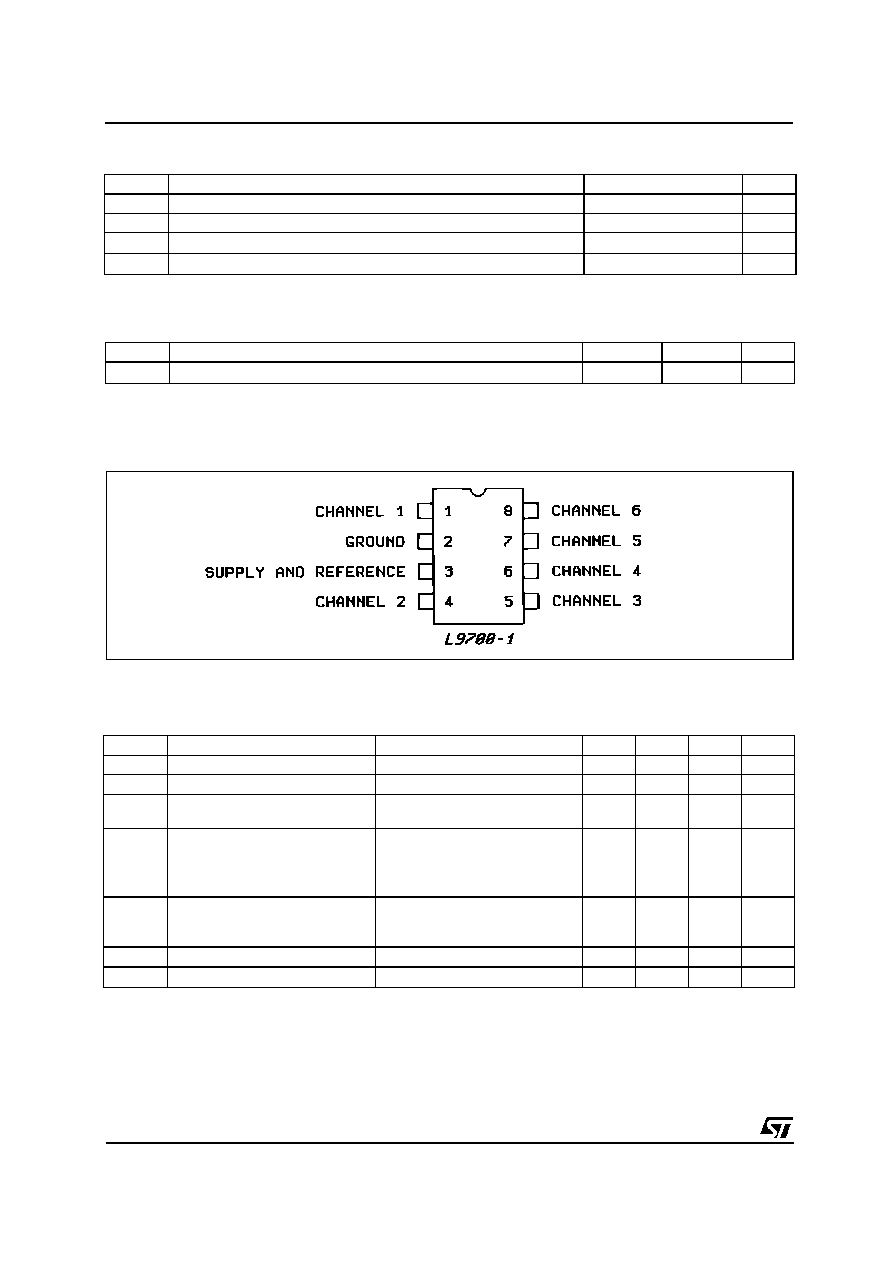
PIN CONNECTION
ABSOLUTE MAXIMUM RATINGS
Symbol
Parameter
Value
Unit
V
CC
Supply Voltage
20
V
I
IN
Input Current per Channel
30
mA
T
j
, T
stg
Junction and Storage Temperature
≠55 to 150
∞
C
P
tot
Total Power Dissipation (T
amb
= 85
∞
C)
650
mW
THERMAL DATA
Symbol
Parameter
MINIDIP
SO8
Unit
R
th j-amb
Thermal Resistance Junction to Ambient Max.
100
200
∞
C/W
ELECTRICAL CHARACTERISTICS (V
CC
= 5V, T
J
= ≠40 to 125
∞
C unless otherwise specified)
Symbol
Parameter
Test condition
Min.
Typ.
Max.
Unit
V
CC
Supply Voltage
4.75
5.25
V
I
CC
Supply Current
1.5
3
mA
V
cis
Static Input Clamping Voltage
Negative I
IN
= ≠10mA
Positive I
IN
= +10mA
≠250
V
CC
0
V
CC
+250
mV
I
IN
Input Current (static)
V
IN
= 0
V
IN
= V
CC
V
IN
= 50mV
V
IN
= V
CC
≠50mV
15
15
5
5
µ
A
µ
A
µ
A
µ
A
V
cld
(*)
Dynamic Input Clamping Voltage
I
IN
=
±
10mA, t
R
= 5ns
Positive Overshoot
Negative Overshoot
400
400
mV
mV
t
S
(*)
Setting Time
See fig. 2
20
ns
R
IN
(*)
Dynamic Input Resistance
5
(*) Design limits are guaranteed by statistical control on production samples over the indicated temperature and supply voltage
ranges. These limits are not used to calculate outgoing quality levels.
Note: The circuit is ESD protected according to MIL-STD-883C
L9700
2/8

Figure 1 : DC INPUT CHARACTERISTIC Limit Points of the Characteristic Approximation.
Figure 2 : Dynamical Input Characteristics.
2a
L9700
3/8

Figure 2 : Dynamical Input Characteristics (continued) .
2b
APPLICATION INFORMATION
Most integrated circuits, both HNMOS and bipolar,
are very sensitive to positive and negative overvol-
tages on the supply and at the inputs.
These transients occur in large numbers and with
different magnitudes in the automotive environment,
making adequate protection for devices ai-med at it
indispensible.
Overvoltages on the supply line are faced through
high voltage integration technologies or through ex-
ternal protection (transil, varistor).
Signal inputs are generally protected using clamp
diodes to the supply and ground, and a current limi-
ter resistor. However, such solutions do not always
completely satisfy the protection specifications in
terms of intervention speed, negative clamping and
current leakage high enough to change analog si-
gnals.
The L9700 device combines a high intervention
speed with a high precision positive and negative
clamp and a low current leakage providing the opti-
mal solution to the problems of the automotive en-
vironment.
The high intervention speed, due to the pre-bias of
the limiter stage and internal feedback, limits the
voltage overshoot and avoid the use of external ca-
pacitors for the limitation of the transient rise times.
Figure 3 illustrates a typical automotive application
scheme. The resistor R
S
limits the input current of
the device and is therefore dimensioned considering
the characteristics of the transients to be eliminated.
Consequently :
V
transient Peak
R
S
=
I
IN MAX
The C
IN
capacitors must be used only on analog in-
puts because they present a low impedance during
the sampling period.
L9700
4/8
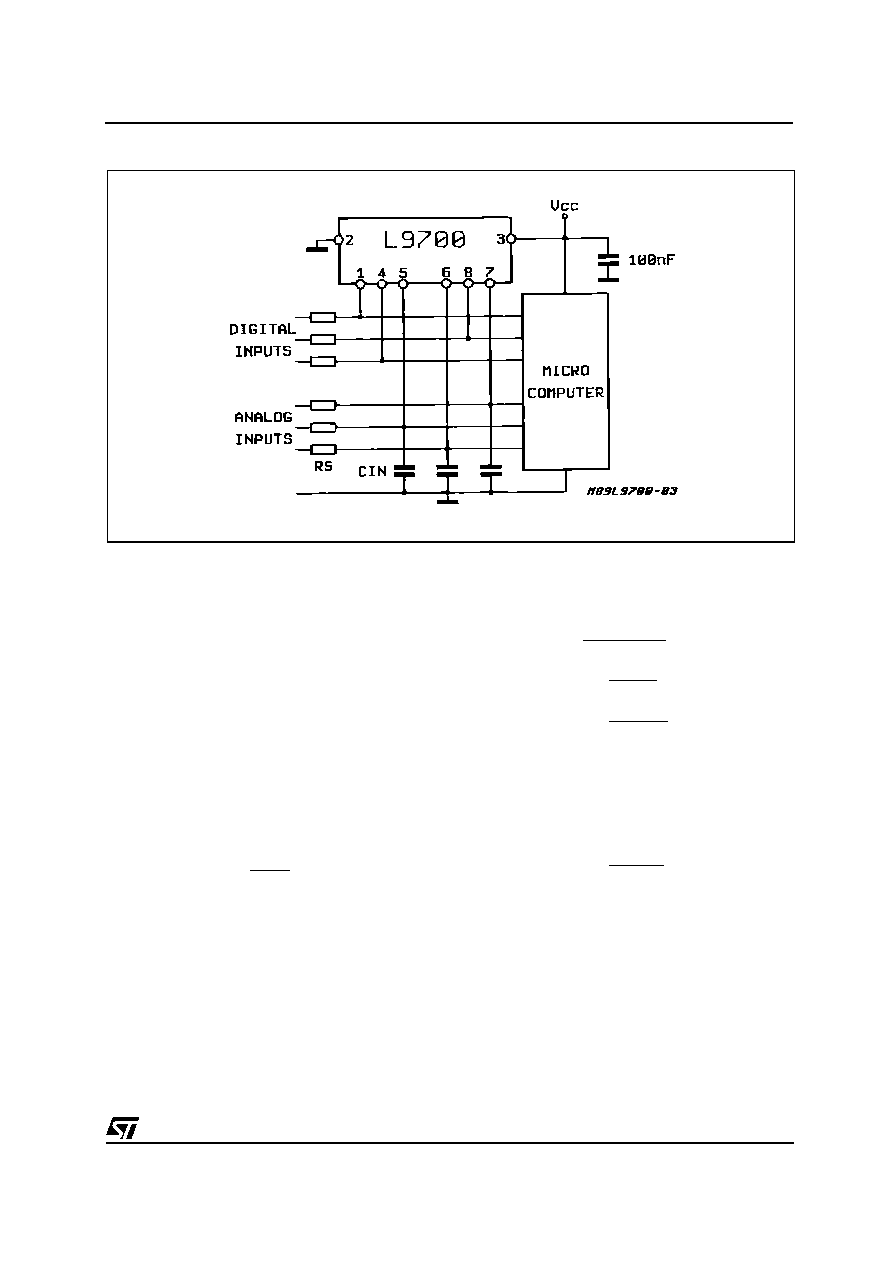
Figure 3 : Typical Application.
The minimum value for C
IN
is determined by the ac-
curacy required, the time taken to sample the input
and the input impedance during that time, while the
maximum value is determined by the required fre-
quency response and the value of R
S
.
Thus for a resistive input A/D connector where :
T
S
=
Sample time (Seconds)
R
D
=
Device input resistance (Ohms)
V
IN
=
Input voltage (Volts)
k
=
Required accuracy (%)
Q
1
=
Charge on capacitor before sampling
Q
2
=
Charge on capacitor after sampling
I
D
=
Device input current (Amps)
Thus :
k
Q
1
Q
1
≠ Q
2
=
100
but Q
1
= C
IN
V
IN
and
Q
1
≠ Q
2
= I
D
≠ T
S
k
C
IN
≠ V
IN
so that
I
D
T
S
=
100
I
D
T
S
and
C
IN
(min) = Farad
V
IN
k
100
T
S
so
C
IN
(min) = Farad
k
R
D
The calculation for a sample and hold type convertor
is even simpler :
k
=
Required accuracy (%)
C
H
=
Hold capacitor (Farad)
100
C
H
C
IN
(min) = Farad
k
L9700
5/8

Minidip
DIM.
mm
inch
MIN.
TYP.
MAX.
MIN.
TYP.
MAX.
A
3.32
0.131
a1
0.51
0.020
B
1.15
1.65
0.045
0.065
b
0.356
0.55
0.014
0.022
b1
0.204
0.304
0.008
0.012
D
10.92
0.430
E
7.95
9.75
0.313
0.384
e
2.54
0.100
e3
7.62
0.300
e4
7.62
0.300
F
6.6
0.260
I
5.08
0.200
L
3.18
3.81
0.125
0.150
Z
1.52
0.060
OUTLINE AND
MECHANICAL DATA
L9700
6/8

DIM.
mm
inch
MIN.
TYP.
MAX.
MIN.
TYP.
MAX.
A
1.75
0.069
a1
0.1
0.25
0.004
0.010
a2
1.65
0.065
a3
0.65
0.85
0.026
0.033
b
0.35
0.48
0.014
0.019
b1
0.19
0.25
0.007
0.010
C
0.25
0.5
0.010
0.020
c1
45
∞
(typ.)
D (1)
4.8
5.0
0.189
0.197
E
5.8
6.2
0.228
0.244
e
1.27
0.050
e3
3.81
0.150
F (1)
3.8
4.0
0.15
0.157
L
0.4
1.27
0.016
0.050
M
0.6
0.024
S
8
∞
(max.)
(1) D and F do not include mold flash or protrusions. Mold flash or
potrusions shall not exceed 0.15mm (.006inch).
SO8
OUTLINE AND
MECHANICAL DATA
L9700
7/8

Information furnished is believed to be accurate and reliable. However, STMicroelectronics assumes no responsibility for the conse-
quences of use of such information nor for any infringement of patents or other rights of third parties which may result from its use. No
license is granted by implication or otherwise under any patent or patent rights of STMicroelectronics. Specification mentioned in this
publication are subject to change without notice. This publication supersedes and replaces all information previously supplied. STMi-
croelectronics products are not authorized for use as critical components in life support devices or systems without express written
approval of STMicroelectronics.
The ST logo is a registered trademark of STMicroelectronics
© 2000 STMicroelectronics ≠ Printed in Italy ≠ All Rights Reserved
STMicroelectronics GROUP OF COMPANIES
Australia - Brazil - China - Finland - France - Germany - Hong Kong - India - Italy - Japan - Malaysia - Malta - Morocco -
Singapore - Spain - Sweden - Switzerland - United Kingdom - U.S.A.
http://www.st.com
L9700
8/8