 | –≠–ª–µ–∫—Ç—Ä–æ–Ω–Ω—ã–π –∫–æ–º–ø–æ–Ω–µ–Ω—Ç: L9911A | –°–∫–∞—á–∞—Ç—å:  PDF PDF  ZIP ZIP |

1/15
L9911
November 2005
This is preliminary information on a new product now in development or undergoing evaluation. Details are subject to change without notice.
1
Features
FULLY MONOLITHIC DESIGN
HIGH SIDE FIELD DRIVER
THERMAL PROTECTION
FIELD SHORT CIRCUIT PROTECTION
PROTECTED DIAGNOSTIC LAMP DRIVER
PROTECTED HIGH SIDE RELAY DRIVER
COMPLEX DIAGNOSTICS
LOAD RESPONSE CONTROL
DFM OUTPUT (FIELD MONITOR)
2
Description
The L9911 is a monolithic multifunction alternator
voltage regulator intended for use in automotive
application. It includes the control section, the field
power stage, fault diagnostic circuit which drives a
warning lamp, and the protection against short cir-
cuits.
3
Circuit Operation
The alternator's voltage regulator performs the fol-
lowing main functions:
≠ 1) voltage regulation
≠ 2) protection
≠ 3) control fault diagnosis
≠ 4) load response control
3.1 VOLTAGE REGULATION
The alternator voltage is compared with a refer-
ence voltage in an amplifier, whose output deter-
mines the switching frequency of output power
MOS whose current excites the coil of the alterna-
tor; as the regulator is in fixed-frequency topology,
the field switching frequency does not depend on
the alternator characteristics. The regulators have
an integrated filter in the voltage sensing path
guaranteeing the correct behaviour of the devices
also when the rectifier diodes feature very high
switching spikes. The internal filtering allows the
usage of the device also with very long cables con-
necting the alternator to the battery with an imped-
ance so high to cause a superimposed ripple on
the alternator voltage higher than 5-6V. Conse-
quently it doesn't need, in the standard applica-
tion, any external component. Anyway an external
capacitor (2.2
µF) must be inserted between A+
and ground when using the device with very long
cables.
3.2 PROTECTION
It is present a protection against short circuits of
the lamp and the relay power drivers (L) and of the
field power driver (F+), a thermal drivers shutdown
protection and an overvoltage protection of L pow-
er drivers.
3.3 DIAGNOSIS
The circuit detects fault conditions related to the
phase and F+ status and receives informations
from one of the three alternator phases. In order to
prevent spurious indications, fault warnings are
not displayed immediately but are dalayed by a
fixed time.
3.4 LOAD RESPONSE CONTROL
The internal circuit regulates the soft start charac-
teristics (activated always at engine start) and the
soft attack characteristics.
PRELIMINARY DATA
CAR ALTERNATOR MULTIFUNCTION SMART VOLTAGE
REGULATOR
Rev. 3
Figure 1. Package
Table 1. Order Codes
Part Number
Package
Features
L9911A
Multiwatt8
See Table.9
L9911B
Multiwatt8
See Table.9
Multiwatt8

L9911
2/15
Figure 2. Pin Connection (Top view)
Table 2. Pin Descriptions
Table 3. Absolute Maximum Ratings (T
j
= -40 to 150∞C, unless otherwise specified)
Table 4. Thermal Data
N∞
Pin
Function
1
P
Phase sense input.
2
DFM
Field monitor output.
3
RES.
Reserved.
4
L
Lamp terminal low side driver; relay terminal high side driver.
5
GND-case
Ground.
6
RES.
Reserved.
7
F
+
High side driver output.
8
B
+
Sensed power supply.
Symbol
Parameter
Value
Unit
V
S
DC Supply Voltage (2 min. @ 25∞C)
24
V
Transient Supply Voltage (load dump) [see application circuit]
t<500ms
40
V
Transient Supply Voltage (low energy spikes) [see application
circuit] ISO7637-1 pulse 1,2,3 /ISO7637-3
60
V
T
j
Junction temperature range
-40 to 150
∞C
T
stg
, T
case
Storage and case temperature range
-40 to 150
∞C
P
tot
Total power Dissipation (@ T
case
150∞C, I
field
5A)
4
W
Reverse Battery Voltage (see application diagram) @ 25∞C, T =
15 sec
-2.5
V
Normal working condition reverse voltage (P vs. GROUND)
-1.5
V
DC Pin Current on F+, B+, GND (bonding limitation)
15
A
ESD Voltage MILSTD883C (All pins vs.GND)
±4
KV
Symbol
Parameter
Value
Unit
R
th j-case
Thermal resistance junction to case
1.5
∞C/W
1
2
3
4
5
6
7
8
P
F
+
GND-case
L
DFM
RE
S.
RE
S.
B
+

3/15
L9911
Table 5. ELECTRICAL CHARACTERISTCS
(T
j
= -40∞C to 150∞C; unless otherwise specified)
Symbol
Parameter
Test Condition
Min.
Typ.
Max.
Unit
Vbat
Operating Supply Voltage
7
18
V
Ib-sinked
Supply Battery Current
25
mA
Ib-stby
Stand-by Current
B+ = 12.5V, F+ = 0V
500
µ
A
Vreg 1
Regulated Voltage & Thermal
Drift.
3 configurations available,
selectable by mask option
(see Table.8).
Ialt=1A-0.9*Inom; Tcase=20∫C;
1400<rpm<RPMMAX (Fig. 3)
14.0
-4.5
14.4
-3.5
14.8
-2.5
V
mV/∞C
Vreg 2
Ialt=10A; Tcase=23∫C;
rpm=6000rpm;15V max (Fig. 4)
14.35
-11.8
14.5
-10
14.65
-8.2
V
mV/∞C
Vreg 3
Ialt=10A; Tcase=23∫C;
rpm=6000rpm (Fig. 5)
14.35
-6
14.5
-4
14.65
-2
V
mV/∞C
Delta
Vrpm
1400<rpm<RPMMAX; Ialt=10A
200
mV
Delta
Vload
5A<Ialt<Inom; rpm=6000rpm
250
mV
Vreg-less
Reg. Voltage without Battery
Ialt = 3A resistive; Tcase=25∫;
2000<rpm<RPMMAX
12
16
V
Vov-p
Overvoltage protection
threshold
Voltage on pin
B+ to disable L
drivers
High and low
side driver off
18
22
V
Vov-d
Overvoltage diagnosis
threshold
VB+ to turn on L low side driver at
VF+ > VS1
Vreg -
5%
Vreg
Vreg +
5%
V
Tj-sd
Thermal shutdown threshold
Temperature to disable F+, DFM, L
(high & low side drivers)
160
175
190
∫C
Tj-sd-dwn
Thermal Shut-down
hysteresis
L/F+/DFM from OFF STATE (due to
thermal shutdown) to ON STATE
Tj-sd-
10
Tj-sd-2
∫C
Vuv-1
Under voltage diagnosis
threshold
VB+ to turn on L low side driver
7.7
8.6
9.5
V
Vuv-up
VB+ to turn off L low side driver
Vuv +
0.40
Vuv +
0.50
Vuv +
0.60
V
VF+_sat
Field driver saturation voltage Tj = 150∫C; I = 4.5A
0.6
V
Tj = 25∫C; I = 7A
0.55
V
Vf
Freewheeling diode F+
I=5A
2
V
If_SCTH
Field short circuit driver
protection threshold current
(see fig. 16
F+ = 0V; Tj = -40∫C
11
18
A
F+ = 0V; Tj = -25∫C
8.5
18
A
F+ = 0V; Tj = -150∫C
5.5
18
A
Vs1
Field driver ON-state
detection
4.5
5.5
V
f-pre
Pre-excitation frequency
283
333
383
Hz
Duty-pre
Pre-excitation Field driver
ON-duty
15.93
18.75
21.57
%
t-rise
Output Voltage Rise Time
Ifield = 3A resistive (Fig. 7)
10
50
µ
s
t_fall
Output Voltage Fall Time
Ifield = 3A resistive (Fig. 7)
10
50
µ
s
Fsw_F+
Field switching frequency
Ialt=1A~0.9*Inom;1400rpm<rpm<R
PMMAX
250
400
Hz
If_leak
Output Field Driver Leakage
Current
B+ = 24V; VF+ = 0
10
µ
A

L9911
4/15
DUTY-PR
Phase regulation max field
ON duty
Fig. 8
26.56
31.25
35.94
%
VH_SAT
High Side Driver Saturation
Voltage (Fig. 10)
With driver Isource=500mA
1.5
V
VL_SAT
Low Side Driver Saturation
Voltage (Fig. 10)
With driver Isink=500mA
1.5
V
VLSB
Selfbias without supply Lamp
driver Voltage
B+ open; L connected to 12V
through a 50 Ohm resistor
4
V
IHSC
High Side Driver short circuit
current protection
B+ = 12.5V; L = GND
1.2
3
A
ILSC
Low Side Driver short circuit
current (see fig. 16)
B+ = L = 12.5V
1
2
A
VthL
Enable Regulator Supply
Voltage Threshold
0.8
1.15
Ipd_L
L terminal Pull-down Current
when the generator is not
rotating
V
L
= 0.6V
0.4
3.5
mA
I_L_sink
L sink current when the
generator is rotating
P frequency 500Hz; VB+ = 12V
100
µ
A
t-D
Diagnostic Alarm Delay Time
0.2
0.5
s
Vcan-DFM Test mode to cancel soft
start/ attack (voltage)
(Fig. 11)
30
50
V
tcan-DFM
Test mode delay time
(Fig. 11)
25
ms
VPHL1
Enable control voltage input
high threshold
square wave f = 1KHz
0.35
V
VPHL2
Enable control voltage input
low threshold
square wave f = 1KHz
0.25
V
t_PHL1
Enable Control Voltage
Phase Filtering Time
50
115
µ
s
VPHH1
Diagnosis phase loss input
high threshold
8
9
10
V
VPHH2_1
Diagnosis phase loss input
low threshold
6.4
7.4
8.4
V
tPHd
Diagnostic Phase Filtering
Time
50
100
µ
s
I_Pd-P1
Phase Pull-down Current
VP = 0.8V
1
8
mA
f-dfm
DFM Output open drain
switching freq.
Ialt=1A~0.9*Inom;1400rpm<rpm<R
PMMAX; I_sink=14mA
125
200
Hz
VL-DFM
Output low voltage saturation
I-sink=14mA
1.5
V
I-SC_DFM Short circuit current
protection
VB+ = VDFM = 12.5V
50
400
mA
Ilk-DFM
Output leakage current
VDFM=16V at DFM driver OFF
5
µ
A
t-TM
Output voltage rise time
R=1K Ohm (Fig. 7)
0.5
50
µ
s
t-TD
Output voltage fall time
R=1K Ohm (Fig. 7)
0.5
50
µ
s
Table 5. ELECTRICAL CHARACTERISTCS (continued)
(T
j
= -40∞C to 150∞C; unless otherwise specified)
Symbol
Parameter
Test Condition
Min.
Typ.
Max.
Unit

5/15
L9911
Table 6. Load Response Control Parameters
Table 7. Load Response Control Timing Options
Table 8. Correspondence of Frequency (typical values) to Application Features
Considering the overall WW application scenario, there is a direct correspondence between Typical Con-
figurations A/B and regulation curve Vreg-1, and between Typical Configuration C and regulation curves
Vreg-2 and Vreg-3. This is allowing the summary of all possible customizations for L9911 in the table be-
low.
Symbol Parameter
Test
Condition Min.
Typ.
Max.
Unit
t_ST_1
Soft Start Delay Time (Fig.
13) 2 steps available,
selectable by mask option
(see Table.7).
Activated always at engine start
0
s
t_ST_2
1.73
2
2.35
t_SL_1
Soft Attack Time / Soft Start
Time (Fig. 13). 2 steps
available, selectable by mask
option (see Table 7).
From 0 to 100% field duty cycle
2.13
2.5
2.87
s
t_SL_2
7.65
9
10.35
EN-RES
(constant)
Reset frequency range to
enable regulation; Frequency
judged after 4 periods (Fig.
12)
40
50
60
Hz
EN-1
Soft start enable (EN) and
LRC disable (DISAB)
frequency ranges.
4 configurations available,
selectable by mask option
(possible combinations in
Table 8). Always activated at
engine start. Frequencies
judged after 4 periods (Fig.
12)
Tj = 25∫C
Tj = -40 to150∫C
108
102
120
120
132
138
Hz
Hz
EN-2
Tj = 25∫C
Tj = -40 to150∫C
131
124
145
145
159
166
Hz
Hz
EN-3
Tj = 25∫C
Tj= -40 to150∫C
144
136
160
160
176
184
Hz
Hz
EN-4
Tj = 25∫C
Tj = -40 to150∫C
174
165
193
193
212
221
Hz
Hz
DISAB-1
Tj = 25∫C
Tj = -40 to150∫C
270
255
300
300
330
345
Hz
Hz
DISAB-2
Tj = 25∫C
Tj = -40 to150∫C
315
298
350
350
385
402
Hz
Hz
DISAB-3
Tj = 25∫C
Tj = -40 to150∫C
367
347
408
408
449
469
Hz
Hz
DISAB-4
Tj = 25∫C
Tj = -40 to150∫C
420
397
466
466
512
535
Hz
Hz
t_SL = 2.5s
t_SL = 9s
t_ST = 0s
LRC-A
LRC-D
t_ST = 2s
LRC-C
LRC-B
Alternator Revolution Speed (rpm)
6 Pole Pairs
8 Pole Pairs
Typical Configuration
A (Config-A)
Initiate Regulation
1200
EN-1
EN-3
LRC Cut
3000
DISAB-1
DISAB-3
Typical Configuration
B (Config-B)
Initiate Regulation
1450
EN-2
EN-4
LRC Cut
3000
DISAB-1
DISAB-3
Typical Configuration
C (Config-C)
Initiate Regulation
1450
EN-2
EN-4
LRC Cut
3500
DISAB-2
EN-4

L9911
6/15
Table 9. Customization of L9911: Combination of LRC, Regulation, and Application Options
Figure 3. Vreg-1
Figure 4. Vreg-2
Vreg-1 / Config-A
Vreg-1 / Config-B
Vreg-2 / Config-C
Vreg-3 / Config-C
LRC Timing
options
6 Pole
Pairs
8 Pole
Pairs
6 Pole Pairs
8 Pole
Pairs
6 Pole
Pairs
6 Pole
Pairs
6 Pole Pairs
6 Pole
Pairs
LRC-A
L9911B
nya
nya
nya
nya
nya
nya
nya
LRC-B
nya
nya
L9911A
nya
nya
nya
nya
nya
LRC-C
Nya
nya
nya
nya
nya
nya
nya
nya
LRC-D
nya
nya
nya
nya
nya
nya
nya
nya
13.4
13.5
13.6
13.7
13.8
13.9
14
14.1
14.2
14.3
14.4
14.5
14.6
14.7
14.8
14.9
15
15.1
15.2
-40
-30
-20
-10
0
10
20
30
40
50
60
70
80
90
100
110
120
130
140
150
T
V
Min.
Max.
Typ.
14.06V~14,91V @ -5∞C
14.00V~14.80V @ 20∞C
13.42V~14,48V @ 150∞C
12.8
12.9
13
13.1
13.2
13.3
13.4
13.5
13.6
13.7
13.8
13.9
14
14.1
14.2
14.3
14.4
14.5
14.6
14.7
14.8
14.9
15
15.1
-
4
0
-
3
5
-3
0
-
2
5
-2
0
-1
5
-
1
0
-
5
0
5
1
0
1
5
2
0
2
5
3
0
3
5
4
0
4
5
5
0
5
5
6
0
6
5
7
0
7
5
8
0
8
5
9
0
9
5
1
0
0
1
0
5
1
1
0
1
1
5
1
2
0
1
2
5
1
3
0
1
3
5
1
4
0
1
4
5
1
5
0
T
V
Min.
Max.
Typ.
14.60V~15.00V @ -5∞C
14.35V~14.65V @ 23∞C
12.85V~13.66V @ 150∞C

7/15
L9911
Figure 5. Vreg-3
Figure 6. Output Voltage rise/fall time (F+, DFM)
13.5
13.6
13.7
13.8
13.9
14
14.1
14.2
14.3
14.4
14.5
14.6
14.7
14.8
14.9
15
15.1
-40
-30
-20
-10
0
10
20
30
40
50
60
70
80
90
100
110
120
130
140
150
T
V
Min.
Max.
Typ.
14.41V~14.82V @ -5∞C
14.35V~14.65V @ 23∞C
13.59V~14.40V @ 150∞C
90%
10%
t-rise
t-TM
t-fall
t-TD
F+
DFM
Voltage

L9911
8/15
Figure 7. Phase Regulation Characteristics
PRINCIPLE OF PHASE REGULATION:
When VB+ is above the regulated voltage, the field driver is controlled to keep phase peak voltage from
falling below VPHH1.
If phase peak voltage drops below VPHL1, phase regulation does not work.
Figure 8. Application Diagram
Engine
Ign. Switch
W/Lamp
Ifield
F+/DFM
off
on
off
on
off
on
t_SL
t_ST
Field Pre-
excitation
Field
Regulation
Load ON
+
_
L9911
L
B+
F+
P
GND
DFM
to E.C.U.
+Vb / Vcc
ignition
switch
warning lamp
Field
Stator
C

9/15
L9911
Figure 9. High Side/Low side driver saturation
Figure 10. Test mode to cancel soft start/attack
Figure 11. Soft-start enable frequency range
Control
Circuit
Regulator Assy
B+
L
L9911
DFM
Vcan
FILTER (tcan)
AND LATCH
COMP
CANCEL
EN-RES
{
EN-1~4
SOFT-START
ENABLE
FREQUENCY
CONSTANT
(50HZ)

L9911
10/15
Figure 12. Soft start characteristics (always activated at engine start)
Ign. sw
on
off
Time (sec)
Time (sec)
Time (sec)
Time (sec)
Engine speed (rpm)
Field current (A)
W/Lamp
(soft attack inhibition Alt. speed)
(soft start enable Alt. speed)
0.5s min
0.5s min
Soft start
delay time
Soft start
delay time
Soft start
delay time
Soft start
timing
Soft start
timing
Soft start
timing
on
off
Ign. sw on
Starter on
E/G stop
and Ign. sw off
Ign. sw on
Starter on
E/G stop
Starter on
0.15s~0.5s
0.15s~0.5s
Engine start
Engine start
Engine restart
Soft attack inhibition
Alt. speed > E/G speed
Soft attack inhibition
Alt. speed < E/G speed

11/15
L9911
Figure 13. Soft Start/attack Characteristics
Table 10. Fault Detection
The diagnostic result is disabled during the Soft-start delay time t_ST 0...3 and the soft-start / soft attack timing t_SL 0...3
Figure 14. DFMonitor Electrical configuration
Root Cause
Signal
Effect
Test detect
Alternator belt breaking
P
Alternator disexcitation
VP<VPHH1 & VB+<Vreg
Brushes open
P
Alternator disexcitation
VP<VPHH1 & VB+<Vreg
Field Driver Open
P
Alternator disexcitation
VP<VPHH1 & VB+<Vreg
Field interruption
P
Alternator disexcitation
VP<VPHH1 & VB+<Vreg
Field short circuit to the battery
F+
Overvoltage
VF+>VS1 & VB+ > Vov-d
Field short circuit to the ground
P
Alternator disexcitation
VP<VPHH1 & VB+<Vreg
Battery discharge
B+
Undervoltage
VB+<Vuv
Engine
Ign. Switch
W/Lamp
Ifield
F+/DFM
off
on
off
on
off
on
t_SL
t_ST
Field Pre-
excitation
Field
Regulation
Load ON
L9911
Control
Circuit
Field driver
DFMon driver
to the ECU
R
Valim
Test circuit
Field
Alternator
Regulator assy
B+
F+
DFM

L9911
12/15
Figure 15. Short circuit drivers' protection
Field driver, DFmon driver and Relay driver are protected in switching mode (not linear), with a retry time
less than 25ms.
Lamp driver is protected in linear mode, with a retry time of 1s.
Current short circuit (Field driver, Relay driver, DFMon driver)
T< 25ms
Current short circuit (Lamp driver)
Filtering time
Retry time
13/15
L9911
4
Package Information
In order to meet environmental requirements, ST offers these devices in ECOPACK
Æ
packages. These
packages have a Lead-free second level interconnect. The category of second Level Interconnect is
marked on the package and on the inner box label, in compliance with JEDEC Standard JESD97. The
maximum ratings related to soldering conditions are also marked on the inner box label.
ECOPACK is an ST trademark. ECOPACK specifications are available at: www.st.com.
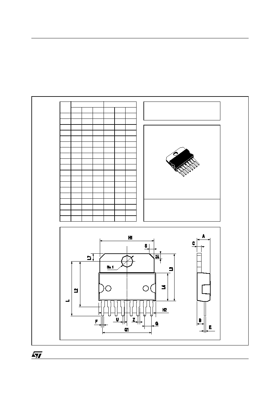
Figure 16. Multiwatt8 Mechanical Data & Package Dimensions
OUTLINE AND
MECHANICAL DATA
0043696 F
DIM.
mm
inch
MIN.
TYP.
MAX.
MIN.
TYP.
MAX.
A
5
0.197
B
2.65
0.104
C
1.6
0.063
E
0.49
0.55
0.019
0.022
F
0.78
0.85
0.030
0.033
G
2.40
2.54
2.68
0.094
0.10
0.105
G1
17.64
17.78
17.92
0.69
0.70
0.71
H1
19.6
0.772
H2
20.2
0.795
L
20.35
20.65
0.80
0.81
L2
17.05
17.20
17.35
0.67
0.68
0.68
L3
17.25
17.5
17.75
0.679
0.689
0.699
L4
10.3
10.7
10.9
0.406
0.421
0.429
L7
2.65
2.9
0.104
0.114
S
1.9
2.6
0.075
0.102
S1
1.9
2.6
0.075
0.102
U
0.40
0.55
0.015
0.022
Z
0.70
0.85
0.028
0.034
Dia1
3.65
3.85
0.144
0.152
Multiwatt8 (Pin 5 GND)

L9911
14/15
Table 11. Revision History
Date
Revision
Description of Changes
June 2004
1
First Issue.
May 2005
2
Modified Figure 2, Table 2 and Table 5;
Updated Figure 10, 11 and 14; Add Table 7.
Add ordering numbers.
07-Nov-2005
3
Updated Table 5.
Added new tables 6-9.

Information furnished is believed to be accurate and reliable. However, STMicroelectronics assumes no responsibility for the consequences
of use of such information nor for any infringement of patents or other rights of third parties which may result from its use. No license is granted
by implication or otherwise under any patent or patent rights of STMicroelectronics. Specifications mentioned in this publication are subject
to change without notice. This publication supersedes and replaces all information previously supplied. STMicroelectronics products are not
authorized for use as critical components in life support devices or systems without express written approval of STMicroelectronics.
The ST logo is a registered trademark of STMicroelectronics.
All other names are the property of their respective owners
© 2005 STMicroelectronics - All rights reserved
STMicroelectronics group of companies
Australia - Belgium - Brazil - Canada - China - Czech Republic - Finland - France - Germany - Hong Kong - India - Israel - Italy - Japan -
Malaysia - Malta - Morocco - Singapore - Spain - Sweden - Switzerland - United Kingdom - United States of America
www.st.com
15/15
L9911