 | –≠–ª–µ–∫—Ç—Ä–æ–Ω–Ω—ã–π –∫–æ–º–ø–æ–Ω–µ–Ω—Ç: LCDP1521 | –°–∫–∞—á–∞—Ç—å:  PDF PDF  ZIP ZIP |
1/8
LCDP1521
Æ
March 2002 - Ed: 1A
DUAL LINE PROGRAMMABLE TRANSIENT VOLTAGE
SUPPRESSOR FOR SLIC PROTECTION
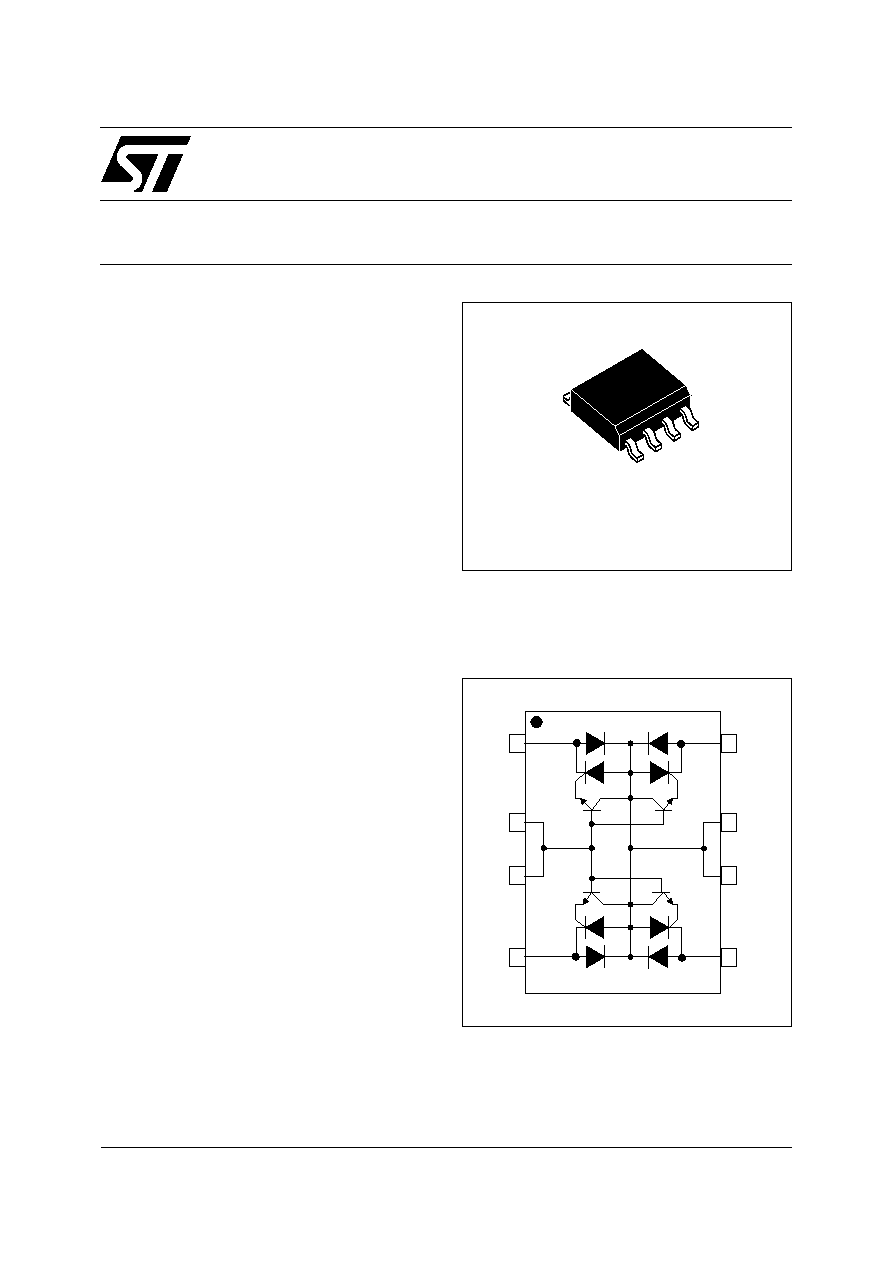
SO-8
s
Dual line programmable transient voltage
suppressor
s
Wide negative firing voltage range:
V
MGL
= -150 V max.
s
Low dynamic switching voltages: V
FP
and V
DGL
s
Low gate triggering current: I
GT
= 5 mA max
s
Peak pulse current: I
PP
= 15 A (10/1000
µ
s)
s
Holding current: I
H
= 150 mA min
FEATURES
This device has been especially designed to
protect 2 new high voltage, as well as classical
SLICs, against transient overvoltages.
Positive overvoltages are clamped by 2 diodes.
Negative surges are suppressed by 2 thyristors,
their breakdown voltage being referenced to -V
BAT
through the gate.
This component presents a very low gate
triggering current (I
GT
) in order to reduce the cur-
rent consumption on printed circuit board during
the firing phase.
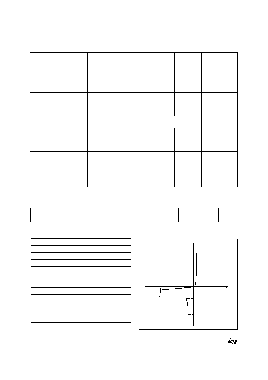
DESCRIPTION
A.S.D.TM
TIP 1
RING 1
TIP 2
RING 2
GATE
GATE
GND
GND
1
2
3
4
8
7
6
5
FUNCTIONAL DIAGRAM
Trisils are not subject to ageing and provide a fail
safe mode in short circuit for a better protection.
Trisils are used to help equipment to meet various
standards such as UL1950, IEC950 / CSA C22.2,
UL1459 and FCC part68. Trisils have UL94 V0
resin approved (Trisils are UL497B approved (file:
E136224)).
BENEFITS
LCDP1521
2/8
STANDARD
Peak Surge
Voltage
(V)
Voltage
Waveform
Required
peak current
(A)
Current
Waveform
Minimum serial
resistor to meet
standard (
)
GR-1089 Core
First level
2500
1000
2/10µs
10/1000µs
500
100
2/10µs
10/1000µs
31
57
GR-1089 Core
Second level
5000
2/10µs
500
2/10µs
62
GR-1089 Core
Intra-building
1500
2/10µs
100
2/10µs
7
ITU-T-K20/K21
6000
1500
10/700µs
150
37.5
5/310µs
200
20
ITU-T-K20
(IEC61000-4-2)
8000
15000
1/60 ns
ESD contact discharge
ESD air discharge
0
0
VDE0433
4000
2000
10/700µs
100
50
5/310µs
120
40
VDE0878
4000
2000
1.2/50µs
100
50
1/20µs
27
0
IEC61000-4-5
4000
4000
10/700µs
1.2/50µs
100
100
5/310µs
8/20µs
120
27
FCC Part 68, lightning
surge type A
1500
800
10/160µs
10/560µs
200
100
10/160µs
10/560µs
43
32
FCC Part 68, lightning
surge type B
1000
9/720µs
25
5/320µs
0
IN COMPLIANCES WITH THE FOLLOWING STANDARDS
Symbol
Parameter
Value
Unit
Rth (j-a)
Junction to ambient
170
∞
C/W
THERMAL RESISTANCE
V
RM
V
R
I
PP
I
H
I
R
I
RM
V
F
I
V
Symbol
Parameter
I
GT
Gate triggering current
I
H
Holding current
I
RM
Reverse leakage current LINE / GND
I
RG
Reverse leakage current GATE / LINE
V
RM
Reverse voltage LINE / GND
V
GT
Gate triggering voltage
V
F
Forward drop voltage LINE / GND
V
FP
Peak forward voltage LINE / GND
V
DGL
Dynamic switching voltage GATE / LINE
V
GATE
GATE / GND voltage
V
RG
Reverse voltage GATE / LINE
C
Capacitance LINE / GND
ELECTRICAL CHARACTERISTICS (T
amb
= 25∞C)
LCDP1521
3/8
Symbol
Parameter
Value
Unit
I
PP
Peak pulse current (see note1)
10/1000
µ
s
8/20µs
10/560µs
5/310
µ
s
10/160µs
1/20µs
2/10
µ
s
15
60
20
25
30
60
70
A
I
TSM
Non repetitive surge peak on-state
current
(50Hz sinusoidal)
t = 10ms
t = 1s
5
3.5
A
I
2
t
I
2
t value for fusing
(50Hz sinusoidal)
t = 10ms
0.125
A
2
s
I
GSM
Maximum gate current
(50Hz sinusoidal)
t = 10ms
2
A
V
MLG
V
MGL
Maximum voltage LINE/GND
Maximum voltage GATE/LINE
-40∞C < Tamb < +85∞C
-40∞C < Tamb < +85∞C
-150
-150
V
T
stg
Tj
Storage temperature range
Maximum junction temperature
- 55 to + 150
150
∞C
T
L
Maximum lead temperature for soldering during 10s
260
∞C
ABSOLUTE RATINGS (T
amb
= 25∞C, unless otherwise specified).
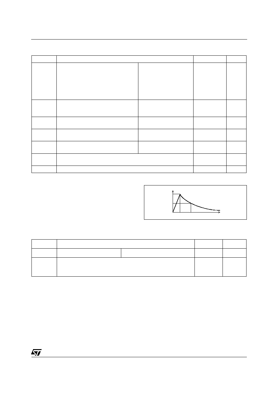
100
50
% IPP
t
t
t
r
p
0
tr: rise time (µs)
tp: pulse duration (µs)
ex: Pulse waveform 10/1000µs
tr = 10µs
tp = 1000µs
Repetitive peak pulse current
Symbol
Test conditions
Max
Unit
V
F
I
F
= 1A
t = 500µs
2
V
V
FP
(note 1)
10/700
µ
s
1.2/50
µ
s
2/10
µ
s
1.5kV
1.5kV
2.5kV
R
S
= 110
R
S
= 60
R
S
= 245
I
PP
= 10A
I
PP
= 15A
I
PP
= 10A
5
10
20
V
Note 1: see test circuit for VFP; RS is the protection resistor located on the line card.
PARAMETERS RELATED TO THE DIODE LINE / GND (T
amb
= 25∞C)
LCDP1521
4/8
Symbol
Test conditions
Typ.
Max.
Unit
I
RM
V
GATE / LINE
= -1V
V
RM
= -150V
V
GATE / LINE
= -1V
V
RM
= -150V
Tc=25∞C
Tc=85∞C
5
50
µ
A
C
V
R
= 50V bias, V
RMS
= 1V, F = 1MHz
V
R
= 2V bias, V
RMS
= 1V, F = 1MHz
20
48
pF
PARAMETERS RELATED TO DIODE AND PROTECTION THYRISTOR (T
amb
= 25∞C, unless otherwise
specified)
Symbol
Test conditions
Min
Max
Unit
I
GT
V
GND / LINE
= -48V
0.1
5
mA
I
H
V
GATE
= -48V (note 2)
150
mA
V
GT
at I
GT
2.5
V
I
RG
V
RG
= -150V
V
RG
= -150V
Tc=25∞C
Tc=85∞C
5
50
µA
V
DGL
V
GATE
= -48V
(note 3)
10/700µs
1.2/50µs
2/10µs
1.5kV
1.5kV
2.5kV
R
S
= 110
R
S
= 60
R
S
= 245
I
PP
= 10A
I
PP
= 15A
I
PP
= 10A
5
10
20
V
Note 2: see functional holding current (IH) test circuit
Note 3: see test circuit for VDGL
The oscillations with a time duration lower than 50ns are not taken into account
PARAMETERS RELATED TO THE PROTECTION THYRISTOR (T
amb
= 25∞C unless otherwise specified)

LCDP1521
5/8
Pulse (µs)
V
p
C
1
C
2
L
R
1
R
2
R
3
R
4
I
PP
R
s
t
r
t
p
(V)
(
µ
F)
(nF)
(
µ
H)
(
)
(
)
(
)
(
)
(A)
(
)
10
700
1500
20
200
0
50
15
25
25
10
110
1.2
50
1500
1
33
0
76
13
25
25
15
60
2
10
2500
10
0
1.1
1.3
0
3
3
10
245
This is a GO-NO GO test which allows to confirm the holding current (I
H
) level in a functional test circuit.
TEST PROCEDURE :
- Adjust the current level at the I
H
value by short circuiting the D.U.T.
- Fire the D.U.T. with a surge current : I
PP
= 10A, 10/1000
µ
s.
- The D.U.T. will come back to the off-state within a duration of 50ms max.
R
V
BAT
= - 100V
Surge generator
D.U.T
FUNCTIONAL HOLDING CURRENT (I
H
) TEST CIRCUIT : GO-NO GO TEST
C
2
R
4
R
3
TIP
RING
GND
V
P
R
2
R
1
L
C
1
(V is defined in unload condition)
P
TEST CIRCUIT FOR V
FP
AND V
DGL
PARAMETERS