
1/9
A.S.D.TM
LCP02-150M
Æ
s
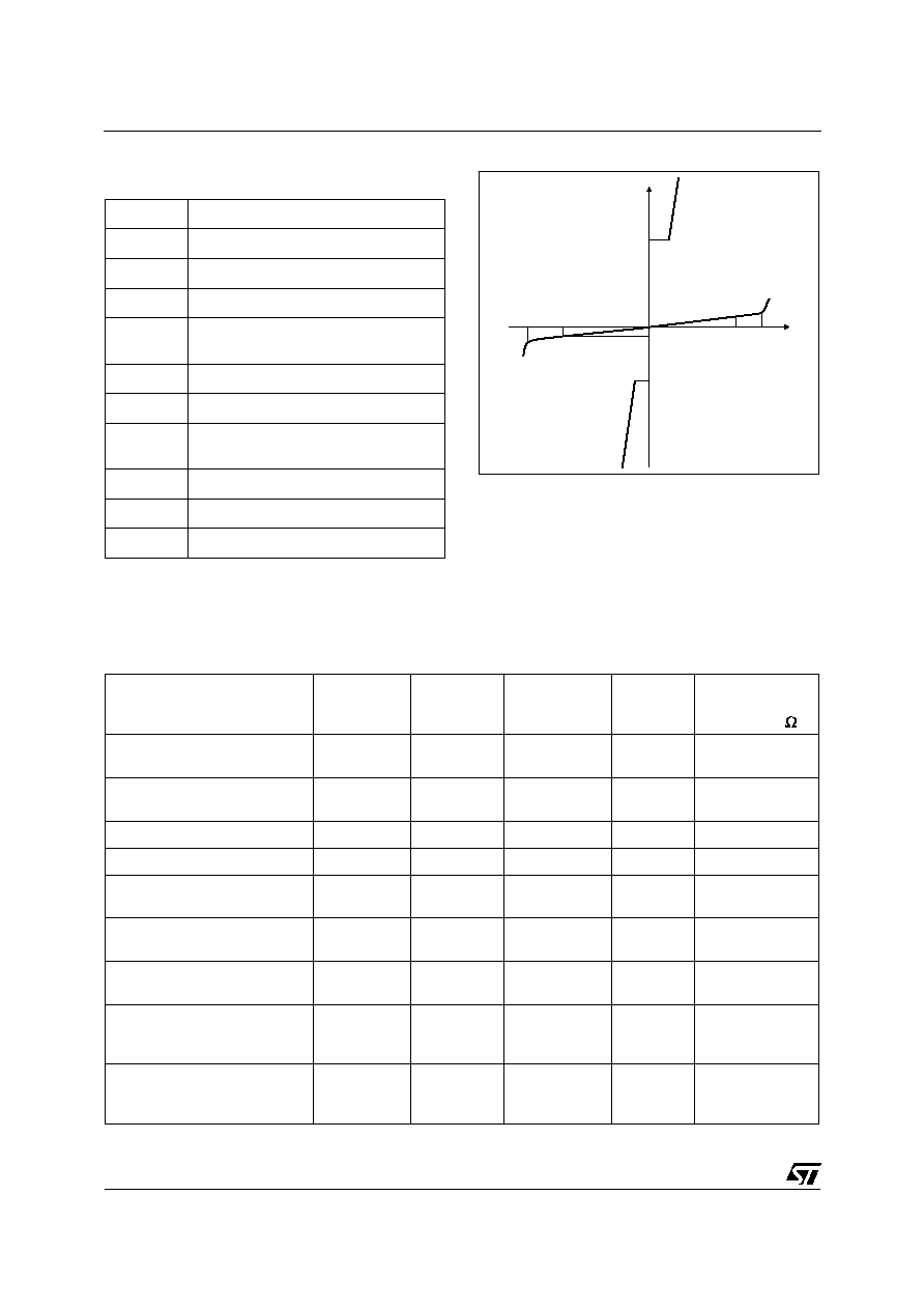
Protection IC recommended for ringing SLICs.
s
Wide firing voltage range: from -110V to +95V.
s
Low gate triggering current
s
Peak pulse current: I
PP
= 100A (10/1000µs) .
s
Holding current: I
H
= 150mA min.
s
High power dissipation capability
s
UL497B approved (file E136224)
FEATURES
PowerS0-10TM
The LCP02-150M has been developed to protect
SLICs operating on both negative and positive
supplies, as well as on high voltage SLICs. It
provides crowbar mode protection for both TIP and
RING lines. Surge suppression is assumed for
each wire by two thyristor structures, one
dedicated to positive surges, the second one to
negative surges. Both positive and negative
threshold levels are programmable by two gates
(Gn and Gp). The use of transistors decreases the
battery currents during surge suppression.
The LCP02-150M has high Bellcore Core, ITU-T
and FCC Part 68 lightning surge ratings, ensuring
rugged performance in the field.
The choice of the PowerSo-10
TM
package is
driven by its high power dissipation capability.
In addition, the LCP02-150M is also specified to
assist a designer to comply with UL1950, IEC950
and CSA C22.2.
It is UL 497B approved (file
E136224), and has UL94-V0 resin approved
DESCRIPTION
May 2003 - Ed: 4B
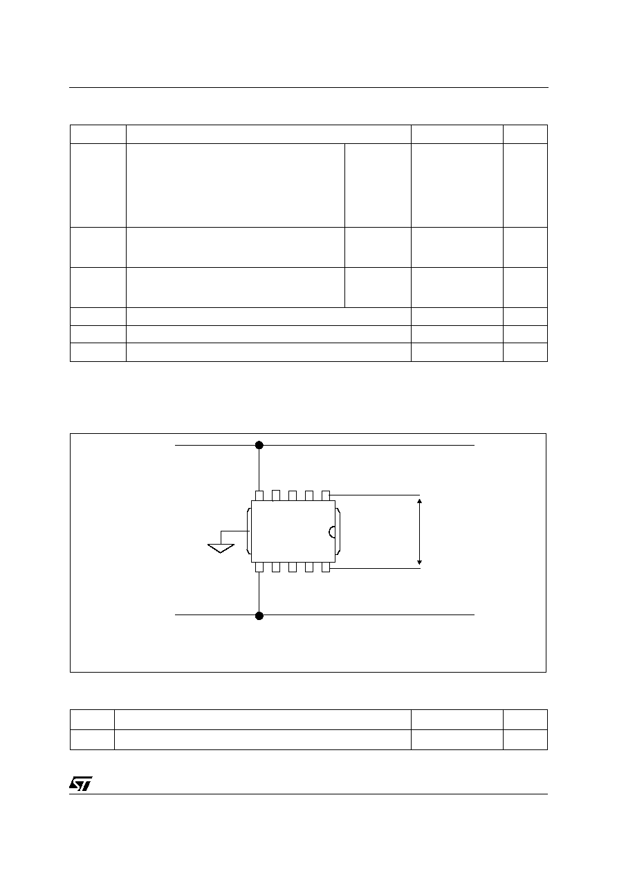
Gn
TIP
Gp
GND
RING
FUNCTIONAL DIAGRAM
TM: ASD is trademarks of STMicroelectronics.
PROGRAMMABLE TRANSIENT VOLTAGE
SUPPRESSOR FOR RINGING SLICS
s
Dual battery supply voltage SLICs
- negative battery supply configuration
- negative & positive battery supply configuration
s
Central Office (CO)
s
Private Branch Exchange (PBX)
s
Digital Loop Carrier (DLC)
s
Asymmetrical Digital Subscriber Line (ADSL)
s
Fiber in the Loop (FITL)
s
Wireless Local Loop (WLL)
s
Hybrid Fiber Coax (HFC)
s
ISDN Terminal Adapter
s
Cable modem
MAIN APPLICATIONS
GND
Gp
TIP
TIP
TIP
TIP
RING
RING
RING
RING
Gn
GND
PIN-OUT CONFIGURATION
LCP02-150M
2/9
Peak surge
voltage
(V)
Voltage
waveform
(µs)
Required
peak current
(A)
Current
waveform
(µs)
Minimum serial
resistor to meet
standard ( )
ITU-T K20
6000
1500
10/700
10/700
150
37.5
5/310
5/310
-
-
ITU-T K21
6000
1500
10/700
10/700
150
37.5
5/310
5/310
-
-
VDE0433
2000
10/700
50
5/310
-
VDE0878
2000
1.2/50
50
1/20
-
IEC61000-4-5
level 4
level 4
10/700
1.2/50
100
100
5/310
8/20
-
-
FCC Part 68
lightning surge type A
1500
800
10/160
10/560
200
100
10/160
10/560
-
-
FCC Part 68
lightning surge type B
1000
9/720
25
5/320
-
BELLCORE
GR-1089-CORE
First level
2500
1000
2/10
10/1000
500
100
2/10
10/1000
-
-
BELLCORE
GR-1089-CORE
Second level
5000
2/10
500
2/10
-
COMPLIES WITH FOLLOWING STANDARDS
Symbol
Parameter
I
GP
Positive gate triggering current
I
GN
Negative gate triggering current
I
H
Holding current
I
RG
Reverse leakage current GATE /
LINE
I
RM
Reverse leakage current
V
RM
Reverse voltage LINE/ GND
V
DGL
Dynamic switching voltage GATE
/ LINE
V
GATE
GATE / GND voltage
V
RG
Reverse voltage GATE / LINE
C
Capacitance LINE / GND
ELECTRICAL CHARACTERISTICS (Tamb = 25∞C)
I
H
I
H
I
RM
I
RM
V
RM
V
GP
V
RM
V
GN
LCP02-150M
3/9
Symbol
Parameter
Value
Unit
R
th (j-a)
Junction to ambient
60
∞
C/W
THERMAL RESISTANCE
TIP
RING
Gn from -110V to +0V
Gp from +0V to +95V
Vbat
190V
Gn connected to negative supply voltage
Gp connected to positive supply voltage
V t: differential voltage between V
and V
ba
Gp
Gn
Gp
Gn
TIP
TIP
TIP
TIP
RING
RING
RING
RING
GND
GND
Fig. 1: Test circuit
Symbol
Parameter
Value
Unit
I
PP
Peak pulse current
10/1000µs
8/20µs
10/560µs
5/310µs
10/160µs
1/20µs
2/10µs
100
250
120
150
200
250
500
A
I
TSM
Non repetitive surge peak on-state current
(sinusoidal)
t = 0.2 s
t = 1s
t = 15 min
13
10
3.5
A
V
GN
max
V
GP
max
V
bat
max
Maximum negative battery voltage range
Maximum positive battery voltage range
Total battery supply voltage
See fig.1
-110 to 0
0 to +95
190
V
T
op
Operating temperature range (see note 1)
-20 to +85
∞C
T
stg
Storage temperature range
- 55 to + 150
∞C
T
L
Maximum lead temperature for soldering during 10s
260
∞C
ABSOLUTE RATINGS (T
amb
= 25 ∞C)
Note 1: Within the Top range, the LCP02-150M keeps on operating. The impacts of the ambient temperature are given by derating curves.
LCP02-150M
4/9
Symbol
Test conditions
Min.
Max.
Unit
I
Gn
V
Gn/GND
= -60V
Measured at 50Hz
5
mA
I
H-
Go-No Go test, V
Gn
= -60V
150
mA
I
RGL-
Tj = 25∞C, V
Gn/line
= -190V
5
µA
V
DGL-
V
Gn/GND
= -60V
10/1000µs 1kV R
P
= 25
I
PP
= 30A
10/700µs 2kV R
P
= 25
I
PP
= 30A
1.2/50µs
2kV R
P
= 25
I
PP
= 30A
10
6
12
V
1 - PARAMETERS RELATED TO THE NEGATIVE SUPPRESSOR
Symbol
Test conditions
Min.
Max.
Unit
I
Gp
V
Gp/GND
= 60V
Measured at 50Hz
10
mA
I
RGL+
Tj = 25∞C, V
Gp/line
= +190V
5
µA
V
DGL+
V
Gp/GND
= +60V
10/1000µs 1kV R
P
= 25
I
PP
= 30A
10/700µs 2kV R
P
= 25
I
PP
= 30A
1.2/50µs
2kV R
P
= 25
I
PP
= 30A
12
8
18
V
2 - PARAMETERS RELATED TO THE POSITIVE SUPPRESSOR
Symbol
Test conditions
Typ.
Max.
Unit
I
R
Tj = 25∞C, V
LINE
= +90V, V
GP/LINE
= +1V
Tj = 25∞C, V
LINE
= -105V, V
GN/LINE
= -1V
5
5
µA
C
off
V
R
= -3V, F =1MHz, V
Gp
= 60V, V
Gn
= -60V
150
pF
3 - PARAMETERS RELATED TO LINE/GND
ELECTRICAL CHARACTERISTICS (T
amb
= 25∞C)
LCP02-150M
5/9
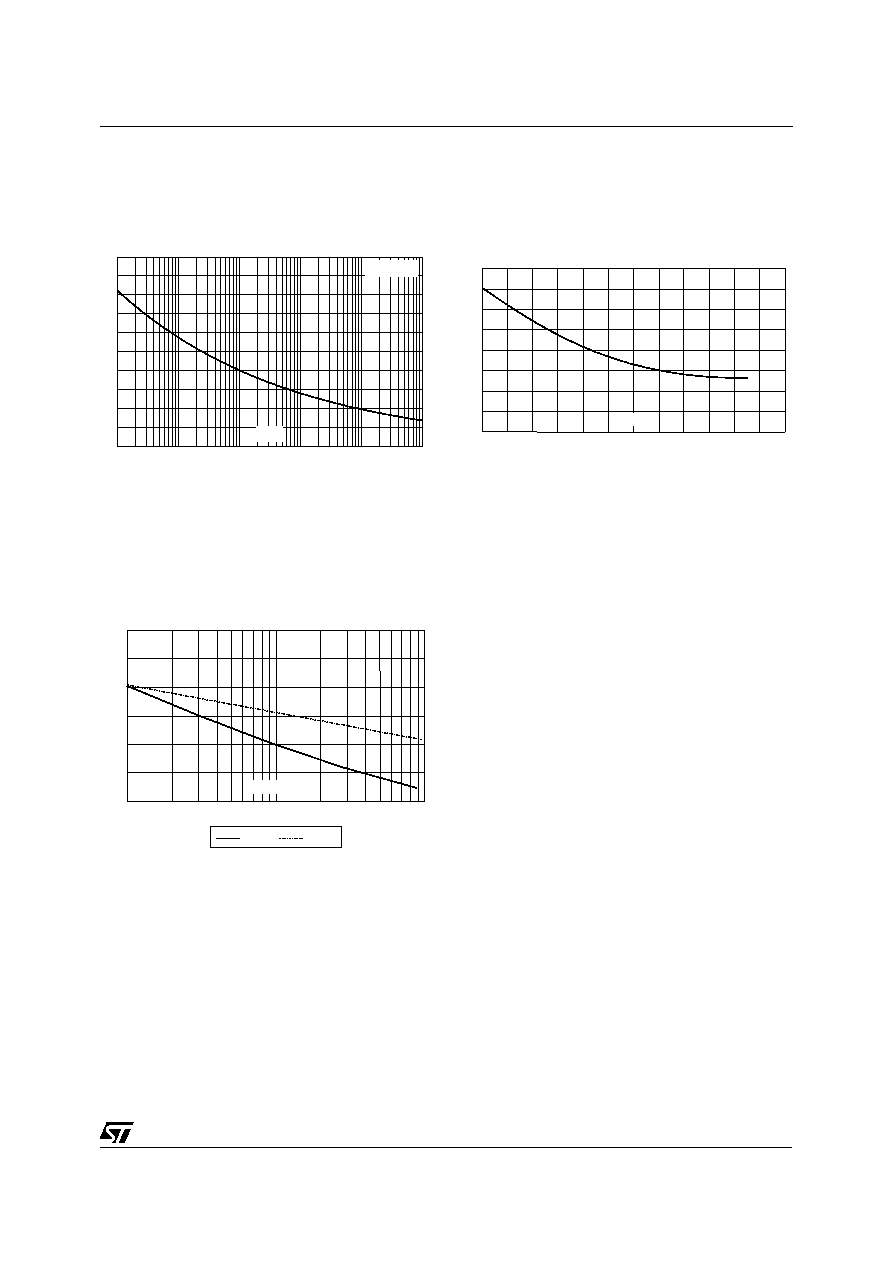
I (T )/I [T =25∞C]
H
j
H
j
0
0.5
1
1.5
2
-20
0
20
40
60
80
100
T(∞C)
Fig. 3: Relative variation of holding current versus
junction temperature.
0.01
0.1
1
10
100
1000
0
5
10
15
20
25
t(s)
I
(A)
TSM
F=50Hz
Tj initial=25C
Fig. 2: Non repetitive surge peak on state current
versus overload duration (Tj initial = 25∞C).
80
100
120
140
160
180
200
1
10
100
Vline (V)
Line -
Line +
Line -
Line +
C(pF)
Fig. 4: Variation of junction capacitance versus re-
verse voltage applied (typical calues) with:
V
GN
= -90V and V
GP
= +90V.