 | –≠–ª–µ–∫—Ç—Ä–æ–Ω–Ω—ã–π –∫–æ–º–ø–æ–Ω–µ–Ω—Ç: LCP1521S | –°–∫–∞—á–∞—Ç—å:  PDF PDF  ZIP ZIP |
Æ
1/11
LCP1521S/LCP152DEE
PROGRAMMABLE TRANSIENT VOLTAGE
SUPPRESSOR FOR SLIC PROTECTION
REV. 4
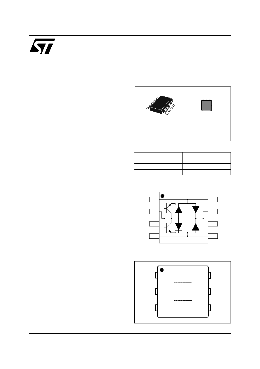
SO-8
LCP1521S
QFN 3x3 6 Leads
LCP152DEE
May 2005
FEATURES
Dual programmable transient suppressor
Wide negative firing voltage range:
V
MGL
= -150 V max.
Low dynamic switching voltages:
V
FP
and V
DGL
Low gate triggering current: I
GT
= 5 mA max
Peak pulse current: I
PP
= 30 A (10/1000 µs)
Holding current: I
H
= 150 mA min
Low space consuming package
DESCRIPTION
These devices have been especially designed to
protect new high voltage, as well as classical
SLICs, against transient overvoltages.
Positive overvoltages are clamped by 2 diodes.
Negative surges are suppressed by 2 thyristors, their
breakdown voltage being referenced to -V
BAT
through the gate.
These components present a very low gate
triggering current (I
GT
) in order to reduce the
current consumption on printed circuit board
during the firing phase.
BENEFITS
TRISILsTM are not subject to ageing and provide a
fail safe mode in short circuit for a better protec-
tion. Trisils are used to help equipment to meet
various standards such as UL60950, IEC950 /
CSA C22.2, UL1459 and FCC part68. Trisils have
UL94 V0 resin approved (Trisils are UL497B ap-
proved [file: E136224]).
Table 1: Order Codes
Part Number
Marking
LCP1521S
CP152S
LCP1521SRL
CP152S
LCP152DEERL
LCP
Figure 1: LCP1521S Functional Diagram
TIP
GATE
NC
RING
TIP
GND
RING
GND
1
Figure 2: LCP152DEE Functional Diagram
TIP
TIP
GATE
GND
NC
RING
RING
TM: TRISIL is a trademark of STMicroelectronics.
ASD
(Application Specific Devices)
LCP1521S/LCP152DEE
2/11
Table 2: Compliances with the following Standards
Table 3: Thermal Resistances
Table 4:
Electrical Characteristics (T
amb
= 25∞C)
STANDARD
Peak Surge
Voltage
(V)
Voltage
Waveform
Required
peak current
(A)
Current
Waveform
Minimum serial
resistor to meet
standard (
)
GR-1089 Core First level
2500
1000
2/10µs
10/1000µs
500
100
2/10µs
10/1000µs
12
24
GR-1089 Core
Second level
5000
2/10µs
500
2/10µs
24
GR-1089 Core
Intra-building
1500
2/10µs
100
2/10µs
0
ITU-T-K20/K21
6000
1500
10/700µs
150
37.5
5/310µs
110
0
ITU-T-K20
(IEC61000-4-2)
8000
15000
1-60ns
ESD contact discharge
ESD air discharge
0
0
VDE0433
4000
2000
10/700µs
100
50
5/310µs
60
10
VDE0878
4000
2000
1.2/50µs
100
50
1/20µs
0
0
IEC61000-4-5
4000
4000
10/700µs
1.2/50µs
100
100
5/310µs
8/20µs
60
0
FCC Part 68, lightning
surge type A
1500
800
10/160µs
10/560µs
200
100
10/160µs
10/560µs
22.5
15
FCC Part 68, lightning
surge type B
1000
9/720µs
25
5/320µs
0
Symbol
Parameter
Value
Unit
R
th(j-a)
Junction to ambient
SO-8
120
∞C/W
QFN
140
Symbol
Parameter
I
GT
Gate triggering current
I
H
Holding current
I
RM
Reverse leakage current LINE / GND
I
RG
Reverse leakage current GATE / LINE
V
RM
Reverse voltage LINE / GND
V
GT
Gate triggering voltage
V
F
Forward drop voltage LINE / GND
V
FP
Peak forward voltage LINE / GND
V
DGL
Dynamic switching voltage GATE / LINE
V
RG
Reverse voltage GATE / LINE
C
Capacitance LINE / GND
V
RM
V
R
I
PP
I
H
I
R
I
RM
V
F
I
V
LCP1521S/LCP152DEE
3/11
Table 5:
Absolute Ratings (T
amb
= 25∞C, unless otherwise specified)
Table 6: Repetitive peak pulse current
Table 7: Parameters related to the diode LINE / GND (T
amb
= 25∞C)
Symbol
Parameter
Value
Unit
I
PP
Peak pulse current
10/1000µs
8/20µs
10/560µs
5/310µs
10/160µs
1/20µs
2/10µs
30
100
35
40
50
100
150
A
I
TSM
Non repetitive surge peak on-state current
(50Hz sinusoidal)
t = 20ms
t = 200ms
t = 1s
12
6
4.5
A
I
GSM
Maximum gate current (50Hz sinusoidal)
t = 10ms
2
A
V
MLG
V
MGL
Maximum voltage LINE/GND
Maximum voltage GATE/LINE
-40∞C < Tamb < +85∞C
-40∞C < Tamb < +85∞C
-150
-150
V
T
stg
T
j
Storage temperature range
Maximum junction temperature
-55 to +150
150
∞C
T
L
Maximum lead temperature for soldering during 10 s.
260
∞C
Symbol
Definition
Example
t
r
Rise time (µs)
Pulse waveform
10/1000µs:
t
r
= 10µs
t
p
= 1000µs
t
p
Pulse duration (µs)
Symbol
Test conditions
Max
Unit
V
F
I
F
= 5A
t = 500µs
3
V
V
FP
(note 1)
10/700µs
1.2/50µs
2/10µs
1.5kV
1.5kV
2.5kV
R
S
= 10
R
S
= 10
R
S
= 62
5
9
30
V
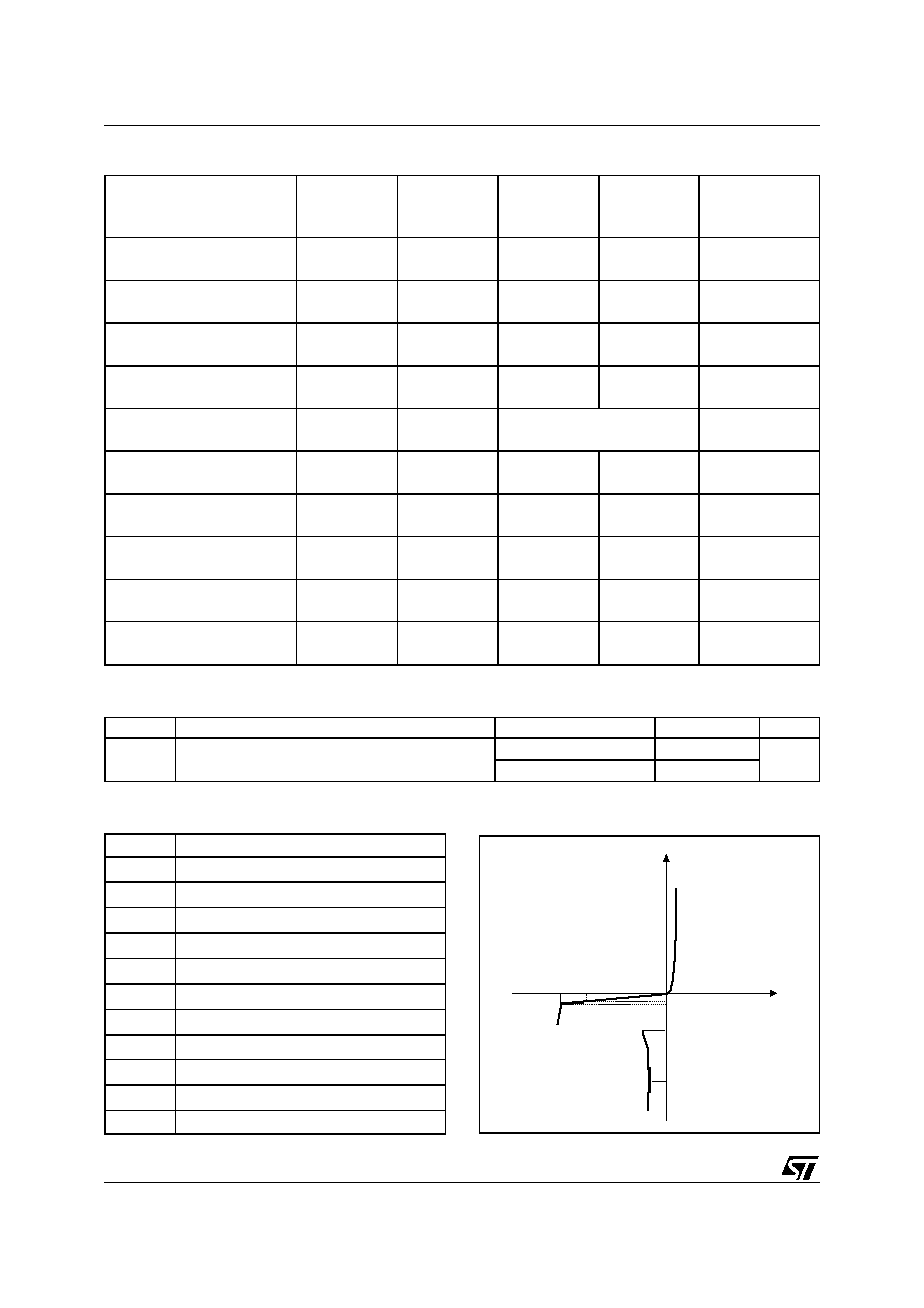
Note 1: see test circuit for VFP; RS is the protection resistor located on the line card.
100
50
% IPP
t
t
t
r
p
0

LCP1521S/LCP152DEE
4/11
Table 8: Parameters related to the protection Thyristors (T
amb
= 25∞C, unless otherwise specified)
Table 9: Parameters related to diode and protection Thyristors
(T
amb
= 25∞C, unless otherwise specified)
Figure 3: Functional Holding Current (I
H
) test circuit: GO-NO GO test
Symbol
Test conditions
Typ
Max
Unit
I
GT
V
GND / LINE
= -48V
0.1
5
mA
I
H
V
GATE
= -48V (note 2)
150
mA
V
GT
at I
GT
2.5
V
I
RG
V
RG
= -150V
V
RG
= -150V
T
j
= 25∞C
T
j
= 85∞C
5
50
µA
V
DGL
V
GATE
= -48V (note 3)
10/700µs
1.2/50µs
2/10µs
1.5kV
1.5kV
2.5kV
R
S
= 10
R
S
= 10
R
S
= 62
I
PP
= 30A
I
PP
= 30A
I
PP
= 38A
7
10
25
V
Note 2: see functional holding current (IH) test circuit
Note 3: see test circuit for VDG
The oscillations with a time duration lower than 50ns are not taken into account.
Symbol
Test conditions
Typ
Max
Unit
I
RM
V
GATE
/ LINE
= -1V V
RM
= -150V
VG
ATE / LINE
= -1V V
RM
= -150V
T
j
= 25∞C
T
j
= 85∞C
5
50
µA
C
V
R
= 50V bias, V
RMS
= 1V, F = 1MHz
V
R
= 2V bias, V
RMS
= 1V, F = 1MHz
15
35
pF
R
V
BAT
= - 100V
Surge generator
D.U.T
This is a GO-NO GO test which allows to confirm the holding current (I ) level in a functional test circuit.
- Adjust the current level at the I value by short circuiting the D.U.T.
- Fire the D.U.T. with a surge current: I
= 10A, 10/1000µs
- The D.U.T. will come back to the off-state within a duration of 50ms max.
H
H
PP
TEST PROCEDURE:

LCP1521S/LCP152DEE
5/11
Figure 4: Test circuit for V
FP
and V
DGL
parameters
TECHNICAL INFORMATION
Figure 5: LCP152 concept behavior
Figure 5 shows the classical protection circuit using the LCP152 crowbar concept. This topology has been
developed to protect the new high voltage SLICs. It allows to program the negative firing threshold while
the positive clamping value is fixed at GND.
When a negative surge occurs on one wire (L1 for example) a current I
G
flows through the base of the
transistor T1 and then injects a current in the gate of the thyristor Th1. Th1 fires and all the surge current
flows through the ground. After the surge when the current flowing through Th1 becomes less negative
than the holding current I
H
, then Th1 switches off.
When a positive surge occurs on one wire (L1 for example) the diode D1 conducts and the surge current
flows through the ground.
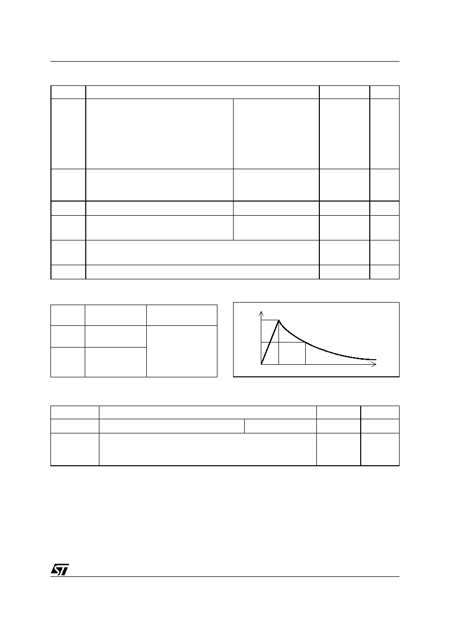
Pulse (µs)
V
p
(V)
C
1
(µF)
C
2
(nF)
L
(µH)
R
1
(
)
R
2
(
)
R
3
(
)
R
4
(
)
I
PP
(A)
R
s
(
)
t
r
t
p
10
700
1500
20
200
0
50
15
25
25
30
10
1.2
50
1500
1
33
0
76
13
25
25
30
10
2
10
2500
10
0
1.1
1.3
0
3
3
38
62
C
C
R
R
TIP
R ING
G ND
V
P
4
3
2
R
2
R
1
(V is defined in unload condition)
P
L
1
V
Ring
GND
Gate
TIP
RING
GND
-Vbat
C
Rs1
Rs2
L 1
L 2
V Tip
Th1
D1
T1
IG
ID1