 | –≠–ª–µ–∫—Ç—Ä–æ–Ω–Ω—ã–π –∫–æ–º–ø–æ–Ω–µ–Ω—Ç: LDO51 | –°–∫–∞—á–∞—Ç—å:  PDF PDF  ZIP ZIP |
1/4
June 2002
IP Library: High PSRR, Low power,
80mA Low Dropout Voltage Regulator
s
ANALOG BASEBAND REGULATOR
s
VERY LOW DROPOUT VOLTAGE : 50mV
s
HIGH PSRR : 60dB
s
LOW QUIESCENT CURRENT : 130
µ
A
s
LOW OUTPUT VOLTAGE NOISE
s
NO CURRENT IN POWER DOWN MODE
s
SHORT CIRCUIT PROTECTION
s
SMALL DECOUPLING CERAMIC CAPACITOR
TYPICAL APPLICATIONS
≠ Cellular and Cordless phones supplied by 1 cell
Lithium-ion battery / 3 cells Ni-MH or Ni-Cd
battery.
≠ PDA (Personal Digital Assistant), Smart phone.
≠ Portable equipment.
≠ Supply for Analog and Mixed-signal devices for
cellular phone.
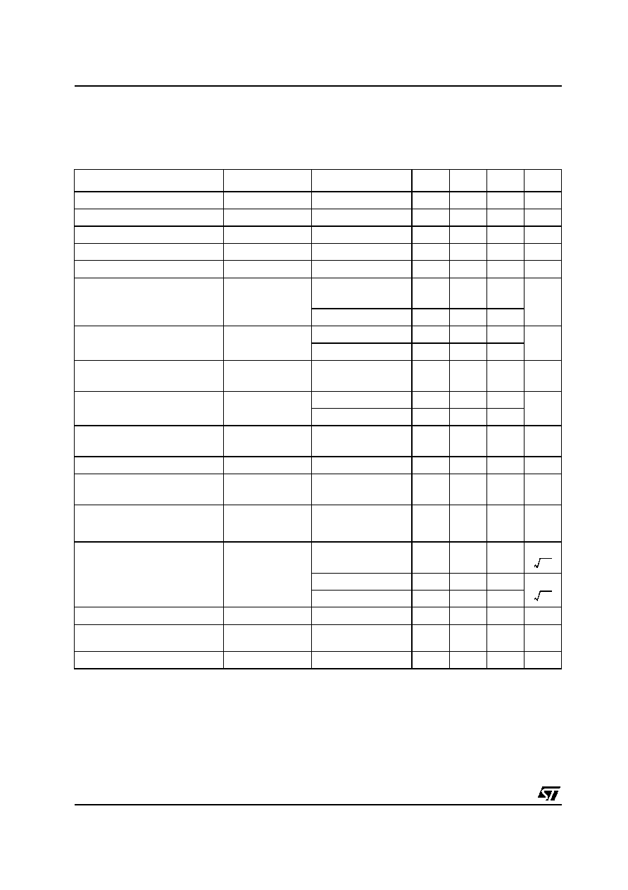
APPLICATION NOTE
An external capacitor (C
OUT
= 1
µ
F) with an
equivalent serial resistance (ESR) in the range
0.02 to 0.6
is used for regulator stability.
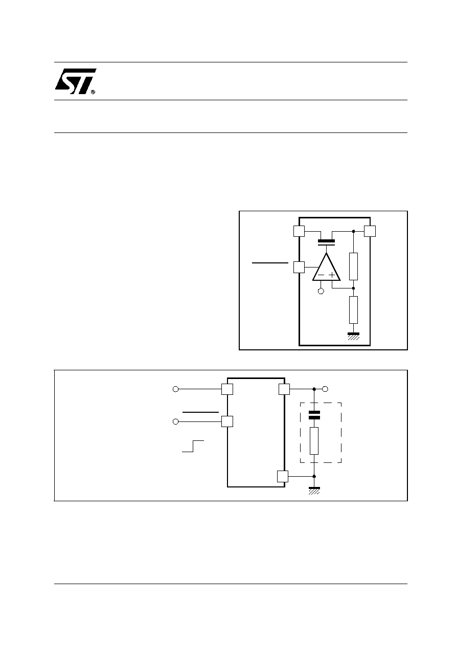
Figure 1 : Block Diagram
?
V
REF
?
?
LDO_51
OUT
IN
PWRDWN
Figure 2 : Typical Application Circuit
1
µ
F
ESR
V
OUT
C
OUT
?
?
OUT
GND
?
?
V
IN
IN
Power Down Mode
OFF
ON
LDO_51
PWRDWN
LDO_51
This is advance information on a new product now in development or undergoing evaluation. Details are subject to change without notice.
PRODUCT PREVIEW
LDO_51
2/4
ELECTRICAL CHARACTERISTICS
3V < V
IN
< 5.5V, -55∞C < T
A
< +125∞C, V
REF
= 2.8V, 0.8
µ
F < C
OUT
< 1.2
µ
F, 20m
< ESR < 0.6
.
100
µ
A < I
LOAD
< 80mA.
Typical case : V
IN
= 4V, T = 25∞C, I
OUT
= 40mA.
Notes: 1. Above characteristics are given for 3V minimum input operating range voltage, but regulator is
operational with 2.7V minimum input voltage.
2. All parameters are guaranteed with 170mV Dropout voltage.
Parameter
Symbol
Test Condition
Min
Typ
Max
Unit
Input Voltage Range (Note 1)
V
IN
3
5,5
V
Output Voltage
V
OUT
2,8
V
Output Voltage Accuracy
-3
3
%
Output current
I
OUT
0,1
80
mA
P
MOS
Output Resistance
R
ON
0,5
Dropout Voltage
V
DO
V
OUT
= 50mV,
I
LOAD
= 80mA
50
mV
(Note 2)
170
Quiescent current
I
Q
I
LOAD
= 100
µ
A
30
50
µ
A
I
LOAD
= 80mA
130
170
Power down mode
quiescent current
I
QPDM
Power down active
100
nA
Power Supply Rejection Ratio
PSRR
f < 10KHz
50
60
dB
f < 100KHz
40
50
Line Regulation
Lir
I
LOAD
= 80mA,
V
IN
= 3V to 5.1V
3
6
mV
Load Regulation
Ldr
30
45
mV
Line Transient
Lirt
V
IN
= 300mV
t
RISE
= t
FALL
= 10
µ
s
1
mV
Load Transient
Ldtr
10% to 90%
and 90% to 10%
of 80mA in 10
µ
s
1
mV
Output Noise Voltage
en
100Hz
1,5
1KHz
550
100KHz
300
Output decoupling Capacitor
C
OUT
1
µ
F
Settling time
From power down to
active mode
25
µ
s
Short Circuit Current Limit
I
SHORT
180
230
300
mA
µ
V
Hz
------------
nV
Hz
------------
LDO_51
3/4
100
1000
10000
100000
0
50
100
150
200
250
300
350
400
450
500
550
600
650
FREQUENCY (Hz)
NO
I
S
E
(
n
Vr
m
s
)
100
1000
10000
100000
20
30
40
50
60
FREQUENCY (Hz)
NO
I
S
E
(
n
Vr
m
s
)
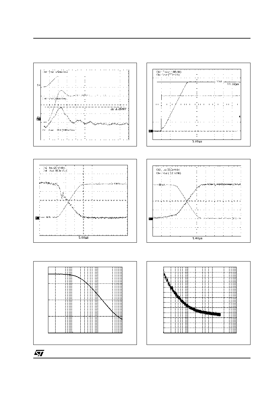
TYPICAL CHARACTERISTICS
Figure 5 : Load Transient (rising edge)
Figure 6 : Load Transient (falling edge)
Figure 7 : PSRR vs Frequency
(I
LOAD
max - V
IN
min)
Figure 8 : Noise vs Frequency
(I
LOAD
max - V
IN
min)
Figure 3 : Line transient
Figure 4 : Settling Time
LDO_51
4/4
Information furnished is believed to be accurate and reliable. However, STMicroelectronics assumes no responsibility for the
consequences of use of such information nor for any infringement of patents or other rights of third parties which may result from
its use. No license is granted by implication or otherwise under any patent or patent rights of STMicroelectronics. Specifications
mentioned in this publication are subject to change without notice. This publication supersedes and replaces all information
previously supplied. STMicroelectronics products are not authorized for use as critical components in life support devices or
systems without express written approval of STMicroelectronics.
The ST logo is a registered trademark of STMicroelectronics
© 2002 STMicroelectronics - All Rights Reserved
STMicroelectronics GROUP OF COMPANIES
Australia - Brazil - Canada - China - Finland - France - Germany - Hong Kong - India - Israel - Italy - Japan - Malaysia - Malta - Morocco
Singapore - Spain - Sweden - Switzerland - United Kingdom - United States
http://www.st.com
20
40
60
80
100
120
OUTPUT CURRENT (mA)
CU
RRE
NT
CO
NS
U
M
P
T
I
O
N (
µ
A
)
0.02
0.1
10
20
30
40
50
60
70
80
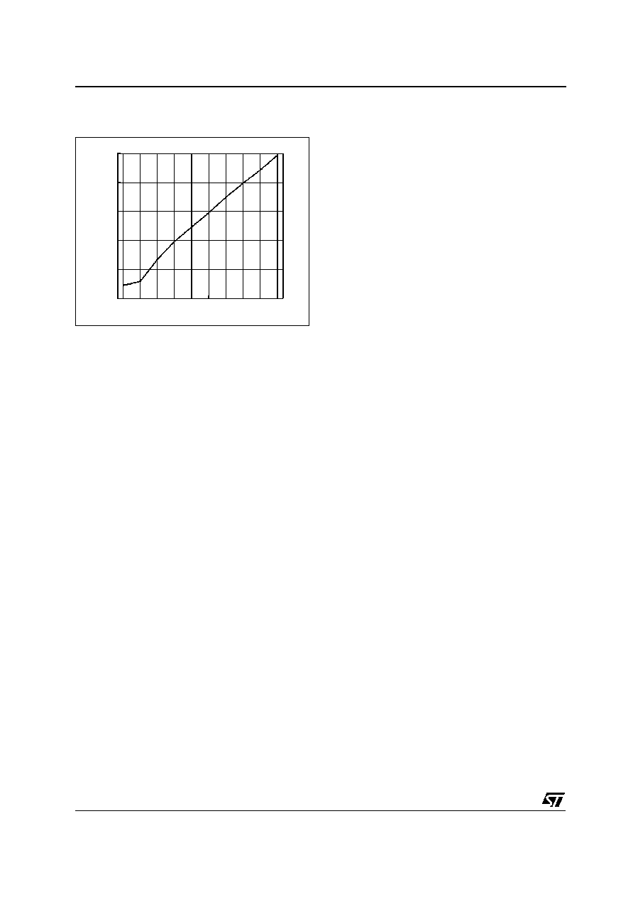
Figure 9 : Current Consumption vs Output Current
(V
IN
= 4V)