1/4
TARGET DATA
February, 27 2003
LET20030S
RF POWER TRANSISTORS
Ldmos Enhanced Technology in Plastic Package
Designed for GSM / EDGE / IS-97 applications
∑ EXCELLENT THERMAL STABILITY
∑ COMMON SOURCE CONFIGURATION
∑ P
OUT
= 30 W with 11 dB gain @ 2000 MHz
∑ ESD PROTECTION
∑ IS-97 CDMA PERFORMANCES
P
OUT
=
4.5 W
EFF = 17 %
DESCRIPTION
The LET20030S is a common source N-Channel,
enhancement-mode lateral Field-Effect RF power
transistor. It is designed for high gain, broad band
commercial and industrial applications. It operates
at 26 V in common source mode at frequencies up
to 2 GHz. LET20030S boasts the excellent gain,
linearity and reliability of ST's latest LDMOS
technology mounted in the first true SMD plastic RF
power package, PowerSO-10RF. LET20030S's
superior linearity performance makes it an ideal
solution for base station applications.
The PowerSO-10 plastic package, designed to offer
high reliability, is the first ST JEDEC approved, high
power SMD package. It has been specially
optimized for RF needs and offers excellent RF
performances and ease of assembly.
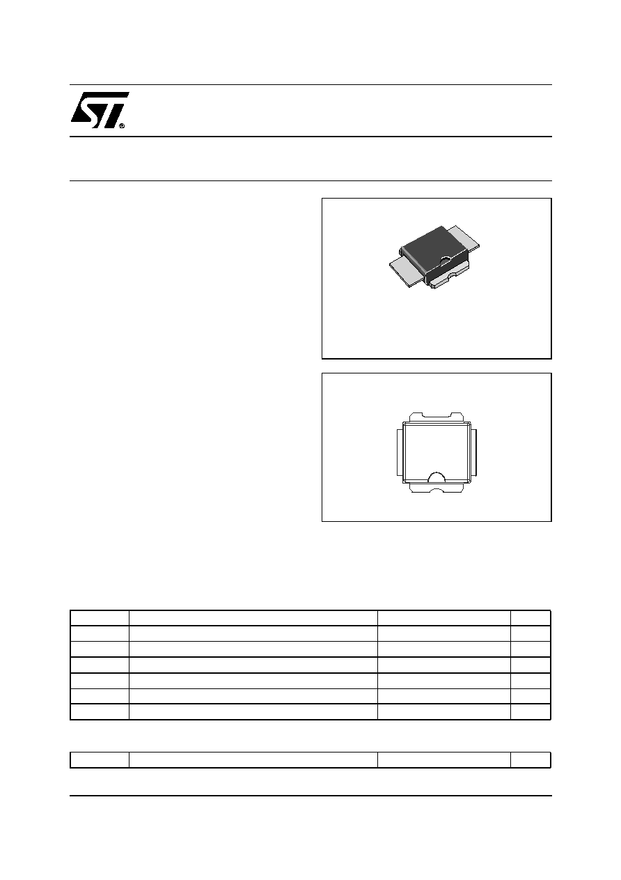
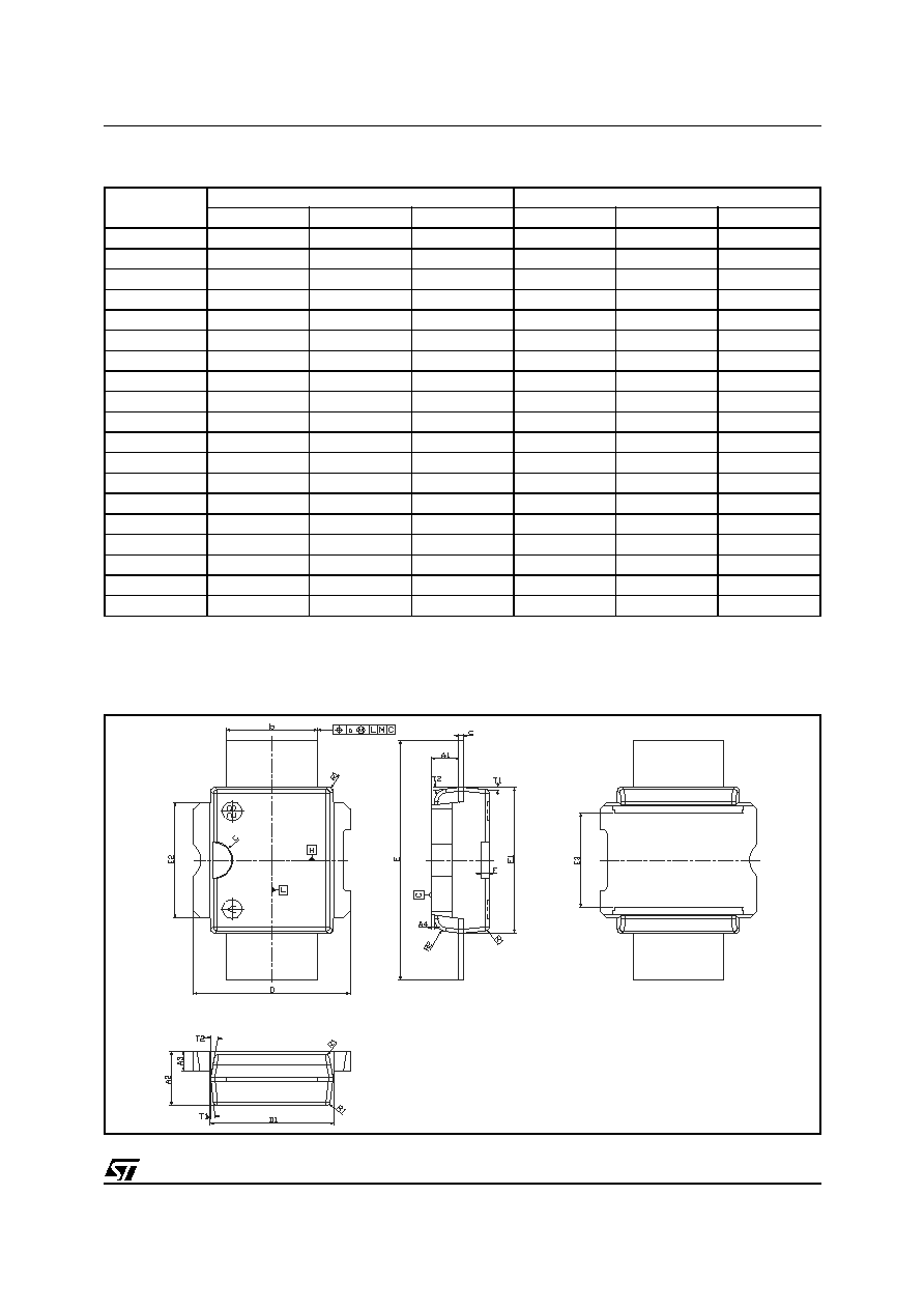
PowerSO-10RF
(straight lead)
BRANDING
LET20030S
ORDER CODE
LET20030S
ABSOLUTE MAXIMUM RATINGS (T
CASE
= 25
∞
C)
Symbol
Parameter
Value
Unit
V
(BR)DSS
Drain-Source Voltage
65
V
V
GS
Gate-Source Voltage
-0.5 to +15
V
I
D
Drain Current
TBD
A
P
DISS
Power Dissipation
140
W
Tj
Max. Operating Junction Temperature
165
∞C
T
STG
Storage Temperature
-65 to +175
∞C
THERMAL DATA
R
th(j-c)
Junction -Case Thermal Resistance
1.0
∞C/W
Mounting recommendations are available in
www.st.com/rf/ (look for application note AN1294)
PIN CONNECTION
GATE
SOURCE
DRAIN

LET20030S
2/4
ELECTRICAL SPECIFICATION (T
CASE
= 25
∞
C)
STATIC
Symbol
Test Conditions
Min.
Typ.
Max.
Unit
V
(BR)DSS
V
GS
= 0 V
I
DS
= 1 mA
65
V
I
DSS
V
GS
= 0 V
V
DS
= 26 V
1
µ
A
I
GSS
V
GS
= 5 V
V
DS
= 0 V
1
µ
A
V
GS(Q)
V
DS
= 26 V
I
D
= TBD
2.5
5.0
V
V
DS(ON)
V
GS
= 10 V
I
D
= 1 A
TBD
V
G
FS
V
DS
= 10 V
I
D
= 1 A
TBD
mho
C
ISS
V
GS
= 0 V
V
DS
= 26 V
f = 1 MHz
TBD
pF
C
OSS
V
GS
= 0 V
V
DS
= 26 V
f = 1 MHz
TBD
pF
C
RSS
V
GS
= 0 V
V
DS
= 26 V
f = 1 MHz
TBD
pF
Symbol
Test Conditions
Min.
Typ.
Max.
Unit
DYNAMIC (
f = 2000 MHz
)
P
1dB
V
DD
= 26 V I
DQ
= TBD
30
W
G
P
V
DD
= 26 V
I
DQ
= TBD
P
OUT
= 30 W
11
13
dB
D
V
DD
= 26 V
I
DQ
= TBD
P
OUT
= 30 W
45
50
%
IMD3
(1)
V
DD
= 26 V
I
DQ
= TBD
P
OUT
= 30 W PEP
-32
-28
dBc
Load
mismatch
V
DD
= 26 V I
DQ
= TBD
P
OUT
= 30 W
ALL PHASE ANGLES
10:1
VSWR
DYNAMIC
(
f = 1930 - 1990 MHz
)
P
OUT
(2)
V
DD
= 26 V I
DQ
= TBD
25
30
W
G
P
V
DD
= 26 V
I
DQ
= TBD
P
OUT
= 30 W
11
13
dB
D
(2)
V
DD
= 26 V
I
DQ
= TBD
P
OUT
= 30 W
40
45
%
P
out(CDMA)
(3)
885 KHz < -47 dBc
1.25 MHz < -55 dBc
2.25 MHz < -55 dBc
4.5
W
D(CDMA)
(3)
885 KHz < -47 dBc
1.25 MHz < -55 dBc
2.25 MHz < -55 dBc
17
%
(1) f
1
= 2000 MHz, f
2
= 2000.1 MHz
(3) IS-97 CDMA Pilot, Sync, Paging, Traffic, Codes 8 Thru 13
(2) 1 dB Compression point
3/4
LET20030S
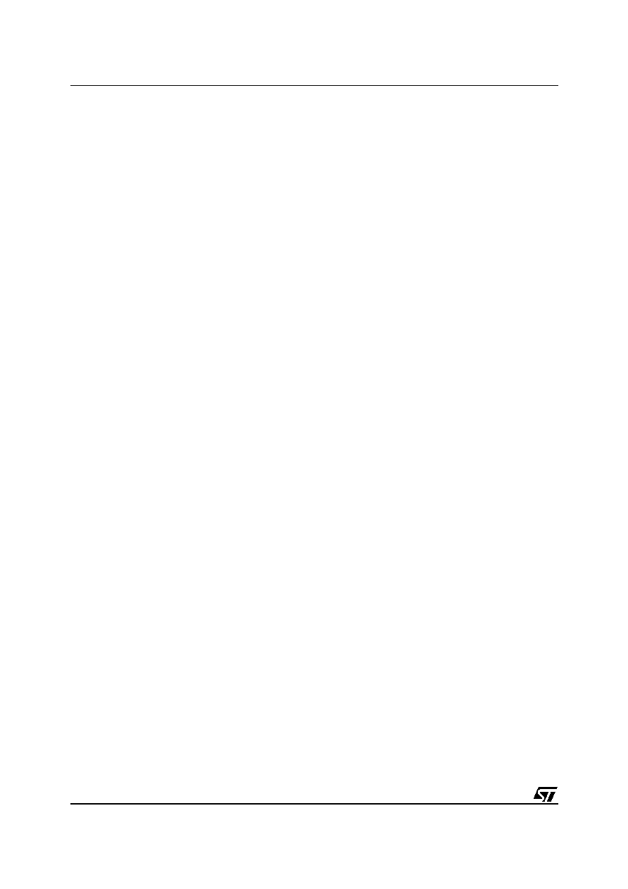
PowerSO-10RF Straight Lead MECHANICAL DATA
CRITICAL DIMENSIONS:
- Overall width (L)
Note (1): Resin protrusions not included (max value: 0.15 mm per side)
mm
Inch
MIN.
TYP.
MAX
MIN.
TYP.
MAX
A1
1.62
1.67
1.72
0.064
0.065
0.068
A2
3.4
3.5
3.6
0.134
0.137
0.142
A3
1.2
1.3
1.4
0.046
0.05
0.054
A4
0.15
0.2
0.25
0.005
0.007
0.009
a
0.2
0.007
b
5.4
5.53
5.65
0.212
0.217
0.221
c
0.23
0.27
0.32
0.008
0.01
0.012
D
9.4
9.5
9.6
0.370
0.374
0.377
D1
7.4
7.5
7.6
0.290
0.295
0.298
E
15.15
15.4
15.65
0.595
0.606
0.615
E1
9.3
9.4
9.5
0.365
0.37
0.375
E2
7.3
7.4
7.5
0.286
0.292
0.294
E3
5.9
6.1
6.3
0.231
0.24
0.247
F
0.5
0.019
G
1.2
0.047
R1
0.25
0.01
R2
0.8
0.031
T1
6 deg
6 deg
T2
10 deg
10 deg
DIM.
LET20030S
4/4
Information furnished is believed to be accurate and reliable. However, STMicroelectronics assumes no responsibility for the consequences
of use of such information nor for any infringement of patents or other rights of third parties which may result from its use. No license is granted
by implication or otherwise under any patent or patent rights of STMicroelectronics. Specifications mentioned in this publication are subject
to change without notice. This publication supersedes and replaces all information previously supplied. STMicroelectronics products are not
authorized for use as critical components in life support devices or systems without express written approval of STMicroelectronics.
The ST logo is registered trademark of STMicroelectronics
Æ
2003 STMicroelectronics - All Rights Reserved
All other names are the property of their respective owners.
STMicroelectronics GROUP OF COMPANIES
Australia - Brazil - Canada - China - Finland - France - Germany - Hong Kong - India - Israel - Italy - Japan -
Malaysia - Malta - Morocco - Singapore - Spain - Sweden - Switzerland - United Kingdom - U.S.A.
http://www.st.com